Dynamic Control of Nonequilibrium Metal–Insulator Transitions
Abstract
We demonstrate a first order metal–insulator phase transition in the repulsive, fully frustrated, single-band Hubbard model as a function of the coupling to a fermion bath. Time dependent manipulation of the bath coupling allows switching between metallic and insulating states both across the phase transition and within the coexistence region. We propose a simple nanoelectronic device for experimentally realizing dynamic control of the bath coupling. Analysis of the device characteristics shows that it can act as a two-terminal memristor.
keywords:
correlated electrons, nonequilibrium-phase transition, nanoscience, memristorsStrongly correlated materials (SCMs) such as transition metal oxides exhibit remarkable intrinsic switching properties down to the nanoscale, making them an exciting future alternative to semiconductor technology 1. Hysteretic resistive switching effects driven by electric fields, currents, Joule heating, or photoexcitation have received much experimental 2, 3, 4, 5, 6, 7, 8, 9, 10, 11, 12, 13, 14, 15, 16, 17, 18 and theoretical 19, 20, 21, 22, 23, 24 attention in this context. Applications include both transistors 25, 26, 27, 28, 29, 30 and memristors 31, 32, 33, 34, 35, 36. Additionally, memristive systems based on SCMs promise to enable neuromorphic devices that mimic the behavior of biological neurons 37, 38, 39, 40, 41. It is thought that such devices could offer lower power consumption and comparable—or even faster—switching timescales than traditional semiconductor electronics 42, 43, 44. At the core of such devices is the physics of Mott metal–insulator transitions.
Here, we describe and solve a simple model showing that a Mott metal–insulator transition can be driven by proximity to a metallic region. Furthermore, we propose a potential nanoscale device for realizing this effect and show that switching between the two states of the device can in principle be achieved on 100ps timescales. The device may be operated as either a transistor, where the system is switched fully across the phase transition; or as a memristor, taking advantage of memory effects in the coexistence region.
We study the repulsive, fully frustrated, single-band Hubbard model on the infinite coordination number Bethe lattice, each site of which is coupled to a noninteracting fermion bath 45, 46, 47. The Hamiltonian describing the Hubbard lattice is given by
| (1) |
where creates (annihilates) lattice fermions with spin on site ; is the lattice hopping matrix element; and is the on-site Coulomb repulsion. We use the hopping as our unit of energy, as our unit of time and set . For example, a bare bandwidth of 4 eV would set our unit of time to be 0.66 fs. In the infinite coordination number limit considered here, this model may be solved exactly via the dynamical mean field theory (DMFT) 48, 49 and is known to exhibit a first order Mott metal–insulator transition as a function of the interaction strength 50.
The Hamiltonian describing the baths is given by
| (2a) | ||||
| (2b) | ||||
Here, creates (annihilates) bath fermions coupled to site with spin and quasimomentum , and is the tunneling matrix element describing hopping between the lattice and the baths. The time dependence of the bath hopping is parameterized by a dimensionless coupling strength so that . The effect of the bath is characterized by a coupling density that parameterizes the bath dispersion and tunneling matrix elements . We choose a flat coupling density with soft-edges , with parameters , and . Time dependent manipulation of the bath coupling has previously been introduced as a method to induce cooling of the system 51, 52.
An exact solution of the model is given by the nonequilibrium DMFT mapping 53. DMFT maps the lattice model to an Anderson impurity model with a self-consistently determined hybridization function given by
| (3) | ||||
where is the impurity Green’s function; is the hybridization between the lattice and bath; and is the time-dependent coupling strength. The equations are solved by starting with an initial guess for , evaluating the impurity Green’s function, and iterating. In the coexistence region, the metallic and insulating solutions may be found by choosing a metallic or insulating initialization of the DMFT loop.
For the solution of the impurity model we use the one crossing approximation (OCA) 54, 55 formulated on the three-branch Keldysh–Matsubara contour. In equilibrium the OCA is known to capture the qualitative physics of the Mott transition with reasonable accuracy 56. We further validate our OCA results against numerically exact inchworm QMC57, 58, 59 data in the parameter regime where this is feasible (see supporting information).
The main quantity of interest is the time-dependent spectral function which we calculate within an auxiliary current formalism 60, 61, 62. We are specifically interested in the density of states at the Fermi energy, , which we use to determine whether the system is in a metallic or insulating state.
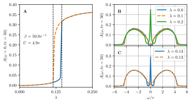
Fig. 1 shows the equilibrium spectral function of the system as a function of the time-independent bath coupling . The interaction strength is set to and the inverse temperature is set to . These parameters are chosen so as to generate a sizable coexistence region, and are used throughout the rest of this paper. The maximum simulation time is set to , which is long enough to resolve sharp features in the spectrum. Fig. 1A shows that increases by several orders of magnitude as is varied from to , for both metallic (dashed orange) and insulating (blue) initializations of the DMFT loop. The system goes through a first order phase transition from an insulating state at small to a metallic state at large . The area between the vertical dashed black lines denotes the coexistence region, where both metallic and insulating solutions are stable, as seen from the gap between the curves representing the two initializations. Fig. 1B shows the full spectral function for several different values of the bath coupling . When the coupling becomes large enough, metallicity is induced and a sharp quasi-particle peak forms at . Finally, Fig. 1C shows the full spectral function for the metallic and insulating solutions within the coexistence region. The two phases remain distinguishable by the presence of a sharp quasiparticle peak in the metal.
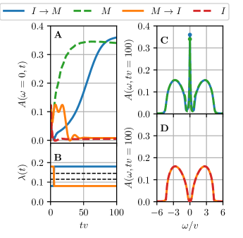
With the equilibrium phase diagram established, we now consider two switching protocols, implemented by time dependent bath couplings , which flip the system between the metallic and insulating phases. In the first switching protocol, the system begins in equilibrium on one side of the phase transition. At time , the bath coupling is rapidly quenched to a value on the opposite side. This switching protocol is described by
| (4) | ||||
where sets the switching rate; sets the switching time; and () sets the initial (final) bath coupling. Fig. 2 shows the effect of this protocol on the system for four pairs of , ): (equilibrium metal), (equilibrium insulator), (“switched” insulator), and (“switched” metal). We take , , , , and . In Fig. 2A we plot the time evolution of . In the metal to insulator transition, the switch rapidly destroys the metal ( is suppressed). In the insulator to metal transition, the system gradually builds up spectral weight at after the switch, eventually roughly matching the equilibrium metal. Figs. 2C and 2D show the full spectral function at for all four realizations of the protocol. The full spectra of the “switched” solutions closely resemble the corresponding equilibrium solutions, demonstrating that the protocol can switch the system between metallic and insulating states.
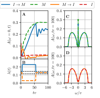
We now consider a second switching protocol in which the system begins in equilibrium in the center of the coexistence region, in either the metallic or insulating phase. At time the bath coupling is rapidly quenched to momentarily place the system outside of the coexistence region on either side of the transition; then, at time , the bath coupling reverts to its initial (coexistence) value. The second switching protocol is described by
| (5) | ||||
where sets the switching rate; and bound the switching interval; and and set the initial/final and intermediate values of the bath coupling, respectively. Fig. 3 shows the results of this switching protocol on the system for three pairs of : , and , where is in the center of the coexistence region, and is large enough to move the system outside of the coexistence region in either direction. The other parameters are given by , , , and . For the equilibrium case we show both the metallic and insulating solutions. Fig. 3A shows the time evolution of the spectral function at the Fermi energy. In the transition, is quickly destroyed during the switch, and does not return when the bath coupling reverts to the coexistence region. In the insulator to metal transition, builds up to almost its equilibrium value during the switching period. Afterwards, the spectral weight drops somewhat, but then recovers and appears to stabilize. Panels C and D of Fig. 3 show the long-time spectral function for each of the four time evolutions. Again, the full spectra of the “switched” solutions closely match the corresponding equilibrium solutions, demonstrating that the second protocol can switch the system between metallic and insulating states within the coexistence region.
We note that for both protocols the overall switching time, assuming a band width of several eV for the SCM, is on the order of 100ps. It is important to realize that this prediction describes only the timescale needed for the electronic transitions to occur, and our minimal model does not consider any other constraints that may appear in experiments. One should also note that this timescale is dominated by the slower transitions to the metallic state, whereas the transitions to the insulating state are substantially faster.
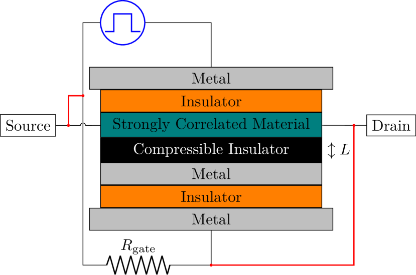
Having demonstrated the ability to dynamically control the phase of our model system through , we shift our attention to potential experimental realizations of this effect. Fig. 4 shows an illustration of a proposed device for achieving dynamic control of . The core of our device consists of a SCM separated from a metal by a nanoscale, compressible, and weakly insulating region possibly composed of several polymer nanolayers. Electronic transport across this region should be dominated by quantum tunneling effects. This core is electrically isolated by two insulating regions and sandwiched between the plates of a capacitor (outer metallic plates). Charging the capacitor generates a force which squeezes the compressible insulator and reduces the separation between the metal and SCM. Since the tunneling rate depends exponentially on the separation, we expect that (at the nanoscale) large variations in can be achieved on fast timescales without the need for very large voltages or compression ratios. This device may be operated in two modes. In the first mode, the gate voltage across the capacitor is externally manipulated (blue signal generator in Fig. 4) to control the source-drain current via the SCM metal–insulator transition, making the device a transistor. In the second mode, the gate voltage across the capacitor is coupled to the source–drain voltage (red connections in Fig. 4), making the device a two terminal memristor.
Due to computational cost, we are only able to fully simulate one switching event. In order to further investigate and characterize the dynamics of the proposed device we consider a simple phenomenological model based on the time-dependent Ginzburg–Landau equations 63. In this framework, we assume that the state of the system around the phase transition is governed by a potential
| (6) |
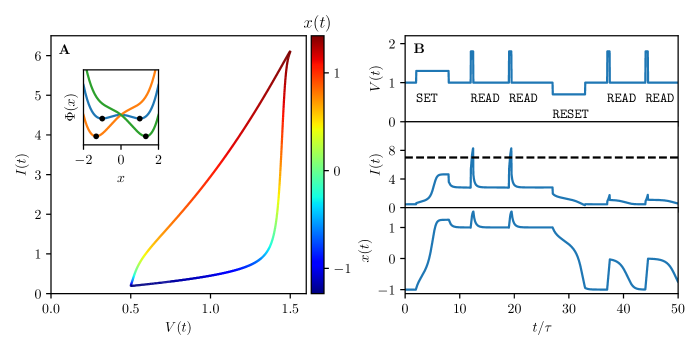
where is at the center of the coexistence region. We take the order parameter to be related to the resistivity of the SCM by . At this potential has two stable minima at corresponding to metallic/insulating states with a resistivity ratio of . The minimal equation of motion for is given by which describes exponential relaxation to equilibrium with timescale .
We now apply this formalism to study the expected characteristics of our proposed device when configured as a memristor. In the memristor setup, the gate voltage across the capacitor is set by the source–drain voltage . We assume that the compression of the insulator is linear in the applied force so that, to leading order, the tunneling rate is given by . Note that since couples to the voltage squared, the device must be operated around a finite bias in order to have bidirectional control over . For the device parameters we set , , and so that at the system is in the center of the coexistence region. Additionally, we set , , and so that the resistivity ratio between the insulating and conducting states is . Finally, we use as our time unit.
Fig. 5A shows the current–voltage characteristics (IV) of the device when driven by a sinusoidal voltage , where we assume that the current through the device is given by Ohm’s law. The IV forms a hysteresis loop due to the memory effect of the order parameter . In the upper part of the loop, we have ; the SCM is in the metallic state; and the current is high. In the lower part of the loop, we have ; the SCM is in the insulating state; and the current is low. Note that the hysteresis loop is not “pinched” (i.e. does not pass through the origin) as expected for ideal memristors 64 because we are operating around a finite voltage bias.
Fig. 5B demonstrates usage of the device as a resistive memory element. The device is operated around a finite voltage bias so that the SCM is in the center of the coexistence region and both high and low resistivity states are stable. The binary state of the device is encoded in the order parameter . Here the device is driven by a sequence of different pulses. The SET pulse is a long low amplitude square pulse which moves the system from the to the state. The READ pulse is a short high amplitude square pulse which causes the current to spike above a threshold (black dashed line) if the SCM is in the low resistivity state. The RESET pulse is a long low amplitude square pulse with opposite polarity to the SET pulse which moves the system from the to the state. Combinations of these pulses allow operation of the device as a two terminal, resistive memory element.
We have demonstrated that the repulsive, fully frustrated, single-band Hubbard model on the infinite coordination number Bethe lattice undergoes a first order metal–insulator transition as a function of a coupling to a set of free fermion baths. By time-dependent manipulation of this coupling we are able to dynamically switch the system between its metallic and insulating states both outside and inside the coexistence region. We propose that this effect may be realized in a nanoscale device based on manipulation of the proximity between a metal and a SCM. Analysis of a simple model of such a device shows that it could be operated as a resistive memory element. These results suggest a variety of directions for future work.
From a theoretical perspective, replacing the OCA impurity solver with a numerically exact method58, 57, 59, 65, 66, 67, 68 would allow us to obtain a better quantitative understanding of the timescales involved in the switching process. It would also be of interest to investigate this type of bath-driven switching in finite dimensional models with more realistic baths and for other metal–insulator transitions, such as the transition between an anti-ferromagnetic insulator and paramagnetic metal seen in .
Experimentally, we expect that a variety of ways to harness this novel switching mechanism in nanoelectronic devices and nanoscale layered materials will emerge. Progress in this direction will rely on finding a compressible insulator with appropriate specifications, and on fabrication techniques. While our results suggest that the fundamental limit on switching and readout time could theoretically be on the order of femtoseconds, it remains to be seen whether other limitations and engineering considerations might dominate in practical setups. Nevertheless, the promise of being able to fabricate an efficient single-crystal memristor is certain to make the experimental challenges worth facing.
JK, EG, and IK were supported by DOE ER 46932 and by the Simons Collaboration on the Many-Electron Problem. G.C. acknowledges support by the Israel Science Foundation (Grant No. 1604/16). International collaboration was supported by Grant No. 2016087 from the United States–Israel Binational Science Foundation (BSF).
-
•
Comparison between the one crossing approximation and inchworm QMC.
References
- Takagi and Hwang 2010 Takagi, H.; Hwang, H. Y. An Emergent Change of Phase for Electronics. Science 2010, 327, 1601–1602, DOI: 10.1126/science.1182541
- Ruzmetov et al. 2009 Ruzmetov, D.; Gopalakrishnan, G.; Deng, J.; Narayanamurti, V.; Ramanathan, S. Electrical triggering of metal-insulator transition in nanoscale vanadium oxide junctions. Journal of Applied Physics 2009, 106, 083702, DOI: 10.1063/1.3245338
- Zhou et al. 2013 Zhou, Y.; Chen, X.; Ko, C.; Yang, Z.; Mouli, C.; Ramanathan, S. Voltage-Triggered Ultrafast Phase Transition in Vanadium Dioxide Switches. IEEE Electron Device Letters 2013, 34, 220–222, DOI: 10.1109/LED.2012.2229457
- Pickett and Stanley Williams 2012 Pickett, M. D.; Stanley Williams, R. Sub-100 fJ and sub-nanosecond thermally driven threshold switching in niobium oxide crosspoint nanodevices. Nanotechnology 2012, 23, 215202, DOI: 10.1088/0957-4484/23/21/215202
- Chudnovskii et al. 1996 Chudnovskii, F. A.; Odynets, L. L.; Pergament, A. L.; Stefanovich, G. B. Electroforming and Switching in Oxides of Transition Metals: The Role of Metal–Insulator Transition in the Switching Mechanism. Journal of Solid State Chemistry 1996, 122, 95–99, DOI: 10.1006/jssc.1996.0087
- Leroy et al. 2012 Leroy, J.; Crunteanu, A.; Bessaudou, A.; Cosset, F.; Champeaux, C.; Orlianges, J.-C. High-speed metal-insulator transition in vanadium dioxide films induced by an electrical pulsed voltage over nano-gap electrodes. Applied Physics Letters 2012, 100, 213507, DOI: 10.1063/1.4721520
- Ha et al. 2013 Ha, S. D.; Zhou, Y.; Fisher, C. J.; Ramanathan, S.; Treadway, J. P. Electrical switching dynamics and broadband microwave characteristics of VO radio frequency devices. Journal of Applied Physics 2013, 113, 184501, DOI: 10.1063/1.4803688
- Sakai and Kurisu 2008 Sakai, J.; Kurisu, M. Effect of pressure on the electric-field-induced resistance switching of VO planar-type junctions. Physical Review B 2008, 78, 033106, DOI: 10.1103/PhysRevB.78.033106
- Valmianski et al. 2018 Valmianski, I.; Wang, P. Y.; Wang, S.; Ramirez, J. G.; Guénon, S.; Schuller, I. K. Origin of the Current-Driven Breakdown in Vanadium Oxides: Thermal versus Electronic. Phys. Rev. B 2018, 98, 195144, DOI: 10.1103/PhysRevB.98.195144
- Stoliar et al. 2013 Stoliar, P.; Cario, L.; Janod, E.; Corraze, B.; Guillot-Deudon, C.; Salmon-Bourmand, S.; Guiot, V.; Tranchant, J.; Rozenberg, M. Universal Electric-Field-Driven Resistive Transition in Narrow-Gap Mott Insulators. Advanced Materials 2013, 25, 3222–3226, DOI: 10.1002/adma.201301113
- Janod et al. 2015 Janod, E.; Tranchant, J.; Corraze, B.; Querré, M.; Stoliar, P.; Rozenberg, M.; Cren, T.; Roditchev, D.; Phuoc, V. T.; Besland, M.-P.; Cario, L. Resistive Switching in Mott Insulators and Correlated Systems. Advanced Functional Materials 2015, 25, 6287–6305, DOI: 10.1002/adfm.201500823
- Giorgianni et al. 2019 Giorgianni, F.; Sakai, J.; Lupi, S. Overcoming the thermal regime for the electric-field driven Mott transition in vanadium sesquioxide. Nature Communications 2019, 10, 1159, DOI: 10.1038/s41467-019-09137-6
- Diener et al. 2018 Diener, P.; Janod, E.; Corraze, B.; Querré, M.; Adda, C.; Guilloux-Viry, M.; Cordier, S.; Camjayi, A.; Rozenberg, M.; Besland, M.; Cario, L. How a dc Electric Field Drives Mott Insulators Out of Equilibrium. Physical Review Letters 2018, 121, 016601, DOI: 10.1103/PhysRevLett.121.016601
- Cavalleri et al. 2001 Cavalleri, A.; Tóth, C.; Siders, C. W.; Squier, J. A.; Ráksi, F.; Forget, P.; Kieffer, J. C. Femtosecond Structural Dynamics in VO during an Ultrafast Solid-Solid Phase Transition. Physical Review Letters 2001, 87, 237401, DOI: 10.1103/PhysRevLett.87.237401
- Cavalleri et al. 2004 Cavalleri, A.; Dekorsy, T.; Chong, H. H. W.; Kieffer, J. C.; Schoenlein, R. W. Evidence for a structurally-driven insulator-to-metal transition in VO : A view from the ultrafast timescale. Physical Review B 2004, 70, 161102, DOI: 10.1103/PhysRevB.70.161102
- Qazilbash et al. 2007 Qazilbash, M. M.; Brehm, M.; Chae, B.-G.; Ho, P.-C.; Andreev, G. O.; Kim, B.-J.; Yun, S. J.; Balatsky, A. V.; Maple, M. B.; Keilmann, F.; Kim, H.-T.; Basov, D. N. Mott Transition in VO Revealed by Infrared Spectroscopy and Nano-Imaging. Science 2007, 318, 1750–1753, DOI: 10.1126/science.1150124
- Wegkamp et al. 2014 Wegkamp, D.; Herzog, M.; Xian, L.; Gatti, M.; Cudazzo, P.; McGahan, C. L.; Marvel, R. E.; Haglund, R. F.; Rubio, A.; Wolf, M.; Stähler, J. Instantaneous Band Gap Collapse in Photoexcited Monoclinic VO due to Photocarrier Doping. Physical Review Letters 2014, 113, 216401, DOI: 10.1103/PhysRevLett.113.216401
- Liu et al. 2012 Liu, M.; Hwang, H. Y.; Tao, H.; Strikwerda, A. C.; Fan, K.; Keiser, G. R.; Sternbach, A. J.; West, K. G.; Kittiwatanakul, S.; Lu, J.; Wolf, S. A.; Omenetto, F. G.; Zhang, X.; Nelson, K. A.; Averitt, R. D. Terahertz-Field-Induced Insulator-to-Metal Transition in Vanadium Dioxide Metamaterial. Nature 2012, 487, 345–348, DOI: 10.1038/nature11231
- Li et al. 2015 Li, J.; Aron, C.; Kotliar, G.; Han, J. E. Electric-Field-Driven Resistive Switching in the Dissipative Hubbard Model. Phys. Rev. Lett. 2015, 114, 226403, DOI: 10.1103/PhysRevLett.114.226403
- Li et al. 2017 Li, J.; Aron, C.; Kotliar, G.; Han, J. E. Microscopic Theory of Resistive Switching in Ordered Insulators: Electronic versus Thermal Mechanisms. Nano Letters 2017, 17, 2994–2998, DOI: 10.1021/acs.nanolett.7b00286
- Han et al. 2018 Han, J. E.; Li, J.; Aron, C.; Kotliar, G. Nonequilibrium mean-field theory of resistive phase transitions. Physical Review B 2018, 98, 035145, DOI: 10.1103/PhysRevB.98.035145
- Mazza et al. 2016 Mazza, G.; Amaricci, A.; Capone, M.; Fabrizio, M. Field-Driven Mott Gap Collapse and Resistive Switch in Correlated Insulators. Physical Review Letters 2016, 117, 176401, DOI: 10.1103/PhysRevLett.117.176401
- Werner et al. 2017 Werner, P.; Strand, H. U. R.; Hoshino, S.; Eckstein, M. Ultrafast switching of composite order in AC. Physical Review B 2017, 95, 195405, DOI: 10.1103/PhysRevB.95.195405
- Li et al. 2018 Li, J.; Strand, H. U. R.; Werner, P.; Eckstein, M. Theory of photoinduced ultrafast switching to a spin-orbital ordered hidden phase. Nature Communications 2018, 9, 4581, DOI: 10.1038/s41467-018-07051-x
- Newns et al. 1998 Newns, D. M.; Misewich, J. A.; Tsuei, C. C.; Gupta, A.; Scott, B. A.; Schrott, A. Mott transition field effect transistor. Applied Physics Letters 1998, 73, 780–782, DOI: 10.1063/1.121999
- Stefanovich et al. 2000 Stefanovich, G.; Pergament, A.; Stefanovich, D. Electrical switching and Mott transition in VO. Journal of Physics: Condensed Matter 2000, 12, 8837–8845, DOI: 10.1088/0953-8984/12/41/310
- Kim et al. 2004 Kim, H.-T.; Chae, B.-G.; Youn, D.-H.; Maeng, S.-L.; Kim, G.; Kang, K.-Y.; Lim, Y.-S. Mechanism and observation of Mott transition in VO -based two- and three-terminal devices. New Journal of Physics 2004, 6, 52–52, DOI: 10.1088/1367-2630/6/1/052
- Ruzmetov et al. 2010 Ruzmetov, D.; Gopalakrishnan, G.; Ko, C.; Narayanamurti, V.; Ramanathan, S. Three-terminal field effect devices utilizing thin film vanadium oxide as the channel layer. Journal of Applied Physics 2010, 107, 114516, DOI: 10.1063/1.3408899
- Nakano et al. 2012 Nakano, M.; Shibuya, K.; Okuyama, D.; Hatano, T.; Ono, S.; Kawasaki, M.; Iwasa, Y.; Tokura, Y. Collective bulk carrier delocalization driven by electrostatic surface charge accumulation. Nature 2012, 487, 459–462, DOI: 10.1038/nature11296
- Yamada et al. 2013 Yamada, H.; Marinova, M.; Altuntas, P.; Crassous, A.; Bégon-Lours, L.; Fusil, S.; Jacquet, E.; Garcia, V.; Bouzehouane, K.; Gloter, A.; Villegas, J. E.; Barthélémy, A.; Bibes, M. Ferroelectric control of a Mott insulator. Scientific Reports 2013, 3, 2834, DOI: 10.1038/srep02834
- Driscoll et al. 2009 Driscoll, T.; Kim, H.-T.; Chae, B.-G.; Di Ventra, M.; Basov, D. N. Phase-transition driven memristive system. Applied Physics Letters 2009, 95, 043503, DOI: 10.1063/1.3187531
- Pellegrino et al. 2012 Pellegrino, L.; Manca, N.; Kanki, T.; Tanaka, H.; Biasotti, M.; Bellingeri, E.; Siri, A. S.; Marré, D. Multistate Memory Devices Based on Free-standing VO/TiO Microstructures Driven by Joule Self-Heating. Advanced Materials 2012, 24, 2929–2934, DOI: 10.1002/adma.201104669
- Son et al. 2012 Son, M.; Liu, X.; Sadaf, S. M.; Lee, D.; Park, S.; Lee, W.; Kim, S.; Park, J.; Shin, J.; Jung, S.; Ham, M.-H.; Hwang, H. Self-Selective Characteristics of Nanoscale VO Devices for High-Density ReRAM Applications. IEEE Electron Device Letters 2012, 33, 718–720, DOI: 10.1109/LED.2012.2188989
- Wong et al. 2013 Wong, F. J.; Sriram, T. S.; Smith, B. R.; Ramanathan, S. Bipolar resistive switching in room temperature grown disordered vanadium oxide thin-film devices. Solid-State Electronics 2013, 87, 21–26, DOI: 10.1016/j.sse.2013.04.032
- Ye et al. 2018 Ye, Y.; Zhao, J.; Xiao, L.; Cheng, B.; Xiao, Y.; Lei, S. Reversible Negative Resistive Switching in an Individual Fe@AlO Hybrid Nanotube for Nonvolatile Memory. ACS Applied Materials & Interfaces 2018, 10, 19002–19009, DOI: 10.1021/acsami.8b01153
- Bae et al. 2013 Bae, S.-H.; Lee, S.; Koo, H.; Lin, L.; Jo, B. H.; Park, C.; Wang, Z. L. The Memristive Properties of a Single VO2 Nanowire with Switching Controlled by Self-Heating. Advanced Materials 2013, 25, 5098–5103, DOI: 10.1002/adma.201302511
- Pickett et al. 2013 Pickett, M. D.; Medeiros-Ribeiro, G.; Williams, R. S. A scalable neuristor built with Mott memristors. Nature Materials 2013, 12, 114–117, DOI: 10.1038/nmat3510
- Strukov et al. 2008 Strukov, D. B.; Snider, G. S.; Stewart, D. R.; Williams, R. S. The Missing Memristor Found. Nature 2008, 453, 80–83, DOI: 10.1038/nature06932
- Kalcheim et al. 2019 Kalcheim, Y.; Camjayi, A.; del Valle, J.; Salev, P.; Rozenberg, M.; Schuller, I. K. Non-Thermal Resistive Switching in Mott Insulators. arXiv:1908.08555 [cond-mat] 2019,
- del Valle et al. 2017 del Valle, J.; Kalcheim, Y.; Trastoy, J.; Charnukha, A.; Basov, D. N.; Schuller, I. K. Electrically Induced Multiple Metal-Insulator Transitions in Oxide Nanodevices. Phys. Rev. Applied 2017, 8, 054041, DOI: 10.1103/PhysRevApplied.8.054041
- del Valle et al. 2019 del Valle, J.; Salev, P.; Kalcheim, Y.; Schuller, I. K. A Caloritronics-Based Mott Neuristor. arXiv:1903.01062 [physics] 2019,
- Zhou and Ramanathan 2015 Zhou, Y.; Ramanathan, S. Mott Memory and Neuromorphic Devices. Proceedings of the IEEE 2015, 103, 1289–1310, DOI: 10.1109/JPROC.2015.2431914
- Yang et al. 2011 Yang, Z.; Ko, C.; Ramanathan, S. Oxide Electronics Utilizing Ultrafast Metal-Insulator Transitions. Annual Review of Materials Research 2011, 41, 337–367, DOI: 10.1146/annurev-matsci-062910-100347
- Brockman et al. 2014 Brockman, J. S.; Gao, L.; Hughes, B.; Rettner, C. T.; Samant, M. G.; Roche, K. P.; Parkin, S. S. P. Subnanosecond Incubation Times for Electric-Field-Induced Metallization of a Correlated Electron Oxide. Nature Nanotechnology 2014, 9, 453–458, DOI: 10.1038/nnano.2014.71
- Han and Li 2013 Han, J. E.; Li, J. Energy dissipation in a dc-field-driven electron lattice coupled to fermion baths. Physical Review B 2013, 88, 075113, DOI: 10.1103/PhysRevB.88.075113
- Han 2013 Han, J. E. Solution of electric-field-driven tight-binding lattice coupled to fermion reservoirs. Physical Review B 2013, 87, 085119, DOI: 10.1103/PhysRevB.87.085119
- Mitra and Millis 2008 Mitra, A.; Millis, A. J. Current-driven quantum criticality in itinerant electron ferromagnets. Physical Review B 2008, 77, 220404, DOI: 10.1103/PhysRevB.77.220404
- Metzner and Vollhardt 1989 Metzner, W.; Vollhardt, D. Correlated Lattice Fermions in d = infinity Dimensions. Physical Review Letters 1989, 62, 324–327, DOI: 10.1103/PhysRevLett.62.324
- Georges and Kotliar 1992 Georges, A.; Kotliar, G. Hubbard model in infinite dimensions. Physical Review B 1992, 45, 6479–6483, DOI: 10.1103/PhysRevB.45.6479
- Rozenberg et al. 1994 Rozenberg, M. J.; Kotliar, G.; Zhang, X. Y. Mott-Hubbard transition in infinite dimensions. II. Physical Review B 1994, 49, 10181–10193, DOI: 10.1103/PhysRevB.49.10181
- Werner et al. 2019 Werner, P.; Eckstein, M.; Müller, M.; Refael, G. Light-induced evaporative cooling of holes in the Hubbard model. Nature Communications 2019, 10, 5556, DOI: 10.1038/s41467-019-13557-9
- Werner et al. 2019 Werner, P.; Li, J.; Golež, D.; Eckstein, M. Entropy-cooled nonequilibrium states of the Hubbard model. Physical Review B 2019, 100, 155130, DOI: 10.1103/PhysRevB.100.155130
- Aoki et al. 2014 Aoki, H.; Tsuji, N.; Eckstein, M.; Kollar, M.; Oka, T.; Werner, P. Nonequilibrium dynamical mean-field theory and its applications. Reviews of Modern Physics 2014, 86, 779–837, DOI: 10.1103/RevModPhys.86.779
- Pruschke and Grewe 1989 Pruschke, T.; Grewe, N. The Anderson model with finite Coulomb repulsion. Zeitschrift für Physik B Condensed Matter 1989, 74, 439–449, DOI: 10.1007/BF01311391
- Eckstein and Werner 2010 Eckstein, M.; Werner, P. Nonequilibrium dynamical mean-field calculations based on the noncrossing approximation and its generalizations. Physical Review B 2010, 82, 115115, DOI: 10.1103/PhysRevB.82.115115
- Vildosola et al. 2015 Vildosola, V.; Pourovskii, L. V.; Manuel, L. O.; Roura-Bas, P. Reliability of the one-crossing approximation in describing the Mott transition. Journal of Physics: Condensed Matter 2015, 27, 485602, DOI: 10.1088/0953-8984/27/48/485602
- Cohen et al. 2015 Cohen, G.; Gull, E.; Reichman, D. R.; Millis, A. J. Taming the Dynamical Sign Problem in Real-Time Evolution of Quantum Many-Body Problems. Physical Review Letters 2015, 115, 266802, DOI: 10.1103/PhysRevLett.115.266802
- Antipov et al. 2017 Antipov, A. E.; Dong, Q.; Kleinhenz, J.; Cohen, G.; Gull, E. Currents and Green’s functions of impurities out of equilibrium: Results from inchworm quantum Monte Carlo. Physical Review B 2017, 95, 085144, DOI: 10.1103/PhysRevB.95.085144
- Dong et al. 2017 Dong, Q.; Krivenko, I.; Kleinhenz, J.; Antipov, A. E.; Cohen, G.; Gull, E. Quantum Monte Carlo solution of the dynamical mean field equations in real time. Physical Review B 2017, 96, 155126, DOI: 10.1103/PhysRevB.96.155126
- Sun and Guo 2001 Sun, Q.-f.; Guo, H. Kondo resonance in a multiprobe quantum dot. Physical Review B 2001, 64, 153306, DOI: 10.1103/PhysRevB.64.153306
- Cohen et al. 2014 Cohen, G.; Reichman, D. R.; Millis, A. J.; Gull, E. Green’s functions from real-time bold-line Monte Carlo. Physical Review B 2014, 89, 115139, DOI: 10.1103/PhysRevB.89.115139
- Lebanon and Schiller 2001 Lebanon, E.; Schiller, A. Measuring the out-of-equilibrium splitting of the Kondo resonance. Physical Review B 2001, 65, 035308, DOI: 10.1103/PhysRevB.65.035308
- Hohenberg and Halperin 1977 Hohenberg, P. C.; Halperin, B. I. Theory of dynamic critical phenomena. Reviews of Modern Physics 1977, 49, 435–479, DOI: 10.1103/RevModPhys.49.435
- Chua 2014 Chua, L. If it’s pinched it’s a memristor. Semiconductor Science and Technology 2014, 29, 104001, DOI: 10.1088/0268-1242/29/10/104001
- Profumo et al. 2015 Profumo, R. E. V.; Groth, C.; Messio, L.; Parcollet, O.; Waintal, X. Quantum Monte Carlo for correlated out-of-equilibrium nanoelectronic devices. Physical Review B 2015, 91, 245154, DOI: 10.1103/PhysRevB.91.245154
- Bertrand et al. 2019 Bertrand, C.; Parcollet, O.; Maillard, A.; Waintal, X. Quantum Monte Carlo algorithm for out-of-equilibrium Green’s functions at long times. Physical Review B 2019, 100, 125129, DOI: 10.1103/PhysRevB.100.125129
- Moutenet et al. 2019 Moutenet, A.; Seth, P.; Ferrero, M.; Parcollet, O. Cancellation of vacuum diagrams and the long-time limit in out-of-equilibrium diagrammatic quantum Monte Carlo. Physical Review B 2019, 100, 085125, DOI: 10.1103/PhysRevB.100.085125
- Bertrand et al. 2019 Bertrand, C.; Florens, S.; Parcollet, O.; Waintal, X. Reconstructing Nonequilibrium Regimes of Quantum Many-Body Systems from the Analytical Structure of Perturbative Expansions. Physical Review X 2019, 9, 041008, DOI: 10.1103/PhysRevX.9.041008
See pages - of suppinfo