This is an author-created postprint. The version of record appeared in
Low Temp. Phys. 46, 331–337 (2020); Fiz. Nizk. Temp. 46, 402–409 (2020); https://doi.org/10.1063/10.0000863. ©2020 Authors
Angular magnetic-field dependence of vortex matching in pinning lattices fabricated by focused or masked helium ion beam irradiation of superconducting YBa2Cu3O7-δ thin films
Abstract
The angular dependence of magnetic-field commensurability effects in thin films of the cuprate high-critical-temperature superconductor YBa2Cu3O7-δ (YBCO) with an artificial pinning landscape is investigated. Columns of point defects are fabricated by two different methods of ion irradiation — scanning the focused 30 keV ion beam in a helium ion microscope or employing the wide-field 75 keV He+ beam of an ion implanter through a stencil mask. Simulations of the ion-target interactions and the resulting collision cascades reveal that with both methods square arrays of defect columns with sub-m spacings can be created. They consist of dense point-defect clusters, which act as pinning centers for Abrikosov vortices. This is verified by the measurement of commensurable peaks of the critical current and related minima of the flux-flow resistance vs magnetic field at the matching fields. In oblique magnetic fields the matching features are exclusively governed by the component of the magnetic field parallel to the axes of the columnar defects, which confirms that the magnetic flux is penetrated along the defect columns. We demonstrate that the latter dominate the pinning landscape despite of the strong intrinsic pinning in thin YBCO films.
I Introduction
Most of the superconducting materials belong to the type II class, into which a magnetic field can penetrate as flux quanta , where is Planck’s constant and the elementary charge. These flux quanta are known as Abrikosov vortices, whirls of the supercurrent that confine the magnetic flux into the cylindrical vortex core, a region with vanishing density of superconducting charge carrier pairs. In clean and isotropic bulk superconductors these vortices arrange themselves in a two-dimensional hexagonal lattice with the axes of the vortex cores oriented parallel to the external magnetic field.
In the cuprate high-temperature superconductors (HTSCs) the situation is more complex and vortices can exist in a large range of magnetic fields between a tiny lower critical field mT and a high upper critical field T at temperatures relevant for the present study and for magnetic fields orthogonal to the CuO2 atomic layers. Kobayashi et al. (1988) The high anisotropy of the HTSCs favors a decomposition of the cylindrical vortices into a stack of coupled “pancake” vortices, Clem (1991) which can be visualized, e.g., in Bi2Sr2CaCu2O8. Correa et al. (2019)
The arrangement of vortices in type-II superconductors can be tailored by the introduction of artificial defects as pinning sites for vortices. Those defects can be classified by their dimensionality and can severely disturb the native hexagonal vortex arrangement. Zero-dimensional (0D) point defects can be introduced as tiny non-superconducting impurities in-situ during fabrication Haugan et al. (2004) or by postprocessing with electron Vovk, Khadzhai, and Dobrovolskiy (2019) or light-ion irradiation of HTSCs. Lang and Pedarnig (2010) One-dimensional (1D) defects are commonly created by irradiation with swift heavy ions that produce amorphous channels with diameters of several nm, i.e., a few times the in-plane coherence length. They have been extensively investigated as a tool to enhance the critical current density. Civale (1997) Finally, grain boundaries and, in the prototypical HTSC YBa2Cu3O7-δ (YBCO) also twin planes, can form two-dimensional (2D) defects that can pin vortices.
The dimensionality of the artificial defects is revealed by different angle-dependent behavior in tilted magnetic fields of superconducting properties like the critical current , the vortex-flow resistance , and . While point defects lead to a marginal angular dependence, randomly distributed yet parallel oriented 1D columnar defects cause narrow features in , , and magnetization vs field direction, centered around the magnetic field direction parallel to their symmetry axes. Holzapfel et al. (1993); Prozorov et al. (1994); Silhanek, Civale, and Avila (2002) Similar observations hold for 2D defect planes in YBCO when the magnetic field is rotated through a direction that is oriented parallel to these planes. Roas, Schultz, and Saemann-Ischenko (1990)
In this work, we investigate artificial pinning lattices that are different in two aspects. First, they are neither strictly 0D or 1D, since they consist of dense point defects that form columnar defect clusters (CDs) with diameters at least one order of magnitude larger than the in-plane coherence length nm in YBCO. Sekirnjak et al. (1995) Second, these CDs are arranged in a periodic pattern that gives rise to commensurability effects at matching vortex and defect densities. Such commensurability effects have been primarily studied in metallic superconductors using arrays of holes (antidots) Fiory, Hebard, and Somekh (1978); Lykov (1993); Metlushko et al. (1994, 1998); Kemmler et al. (2006); Misko et al. (2010); Moshchalkov and Fritzsche (2011) or magnetic dots Vélez et al. (2008) in the material, nanogrooves, Shklovskij and Dobrovolskiy (2006, 2008); Dobrovolskiy et al. (2012) and superlattices Dobrovolskiy et al. (2018) but are also found in YBCO perforated with holes. Castellanos et al. (1997)
The fabrication techniques of pinning arrays in our samples are based on the observation that irradiation of YBCO thin films with He+ ions of moderate energy introduces point defects by displacing mainly oxygen atoms. This leads to a reduction of the transition temperature , Wang et al. (1995) which can be well controlled by the ion fluence. Sefrioui et al. (2001); Lang et al. (2004); Lang and Pedarnig (2010); Cybart et al. (2014) By ion irradiation through a shadow mask Lang et al. (2006, 2009); Pedarnig et al. (2010); Swiecicki et al. (2012); Trastoy et al. (2013); Haag et al. (2014); Zechner et al. (2017, 2018a, 2018b) or using the focused ion beam of a He ion microscope (HIM) Aichner et al. (2019) an array of CDs can be created that acts as a pinning landscape for vortices.
Only few investigations have addressed the angular dependence of vortex commensurability effects in metallic superconductors with antidots Metlushko et al. (1998); Womack et al. (2019) and in YBCO thin films patterned with periodic CDs by ion irradiation. Trastoy et al. (2013); Zechner et al. (2018a) The purpose of this study is to explore whether the pinning landscapes created in YBCO by focused He+ ion irradiation in a HIM act as 1D line-like pinning centers despite of consisting of 0D point defect clusters with inhomogeneous density.
II Experimental methods
Epitaxial thin films of YBa2Cu3O7-δ are grown on (100) MgO single-crystal substrates by pulsed-laser deposition using 248 nm KrF-excimer-laser radiation at a fluence of 3.2 J/cm2. The thicknesses of the films used in this work are nm (sample SQ200) and nm (sample SQ500). The critical temperatures of the as-prepared films are K with transition widths K. The films are patterned by photolithography and wet chemical etching to form bridges with a length of and a width of . Electrical contacts in a four-probe geometry are established on side arms of the bridges using sputtered Au pads with a voltage probe distance of .
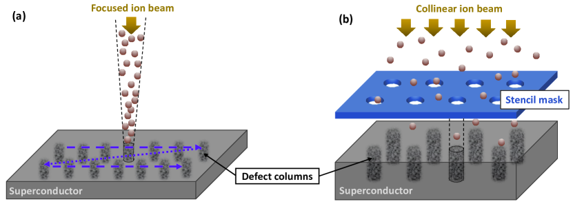
In both samples, a tailored vortex pinning landscape was created by different methods of He+ ion irradiation. Sample SQ200 was irradiated with an intentionally defocused ion beam in a HIM. The setup starts with adjusting the HIM settings to highest resolution and then changing the working distance (beam focus plane) so that the beam hits the sample surface with a nearly Gaussian fluence profile Emmrich et al. (2016) with a full width at half maximum (FWHM) of about 50 nm. Since the aperture angle of the ion beam is very small the ion beam hits the sample surface almost orthogonally. The method is described in detail elsewhere. Aichner et al. (2019)
By sequentially scanning the ion beam over the sample surface, a square lattice of columnar defects with nm spacings is created in the thin YBCO film in an overall area of approximately . Every point is irradiated with 30 keV He+ ions with a dwell time of 2.7 ms and a beam current of 3 pA, corresponding to He+ ions/point. The method is sketched in Fig. 1(a).
Sample SQ500 is patterned by masked ion beam structuring (MIBS) Lang et al. (2006) as sketched in Fig. 1(b). A m-thick Si stencil mask is placed on top of the YBCO film and adjusted in an optical microscope with the help of marker holes. The mask is separated from the surface of the YBCO film by a circumferential spacer layer made of m-thick photoresist. The stencil mask is perforated with holes with diameters nm, arranged in a square array of nm pitch, which covers the entire bridge. The stencil pattern is shadow projected onto the YBCO surface by irradiating the arrangement with a collinear 75 keV He+ ion beam, oriented orthogonal to the sample surface, in a commercial ion implanter (High Voltage Engineering Europa B. V.).
Electrical transport measurements are performed in a closed-cycle cryocooler with temperature control by a Cernox resistor, which has a negligible temperature reading error in moderate magnetic fields. Heine and Lang (1998) The applied magnetic field is supplied by a revolvable electromagnet with angular resolution and is measured by a calibrated Hall probe mounted between the magnet’s pole pieces. The Hall probe is connected to a LakeShore 475 gaussmeter, allowing for measurements of with a zero offset T, and a reading accuracy . The tilt angle is defined as the angle between the surface normal of the YBCO film and the direction of . The angle-dependent magnetoresistance measurements are performed in constant Lorentz force geometry, i. e., the magnetic field is always perpendicular to the current direction. For all measurements the current through the sample is generated by a constant-current source in both polarities to eliminate thermoelectric signals and the voltage is measured by a Keithley 2182A nanovoltmeter. The critical current is determined from isothermal current-voltage () measurements with a voltage criterion of 100 nV, corresponding to V/cm. Since the characteristics of a superconductor are nonlinear the resistance curves presented below are defined as at a fixed . Note that the absolute value of is not important for our analyses.
III Results and discussion
To compare the shapes of the artificial CD lattices, prepared by the two different irradiation methods, simulations of the defect distributions with the program package SRIM/TRIM Ziegler, Littmark, and Biersack (1985); Ziegler, Ziegler, and Biersack (2010) are performed. It computes the impact of ions on solids using a binary collision approximation of ion-atom and atom-atom collisions, and delivers the full collision cascades. However, ion channeling, thermal effects, diffusion, and recrystallization are not considered.
Details of the crystallographic structure are not considered in SRIM/TRIM as it uses a Monte-Carlo method and assumes amorphous targets. For the spatial modulation of superconductivity, the Ginzburg-Landau coherence length is the relevant length parameter and therefore we have determined the average defect density within calculation cells of nm3 — a length scale of the order of the in-plane coherence length of YBCO. Note that the investigated point defect densities are below the amorphization limit and a comparison to an experimental visualization is hardly possible. Only by using a larger ion fluence, amorphous channels can be created and detected in cross-section scanning transmission electron microscopy images.Müller et al. (2019)
The pinning potential for vortices is provided by a local suppression of , which can be calculated from the defect density on the grounds of the pair-breaking theory of Abrikosov and Gor’kov. Abrikosov and Gor’kov (1960) Since annealing effects are not considered in SRIM/TRIM and various other effects may lead to substantial uncertainty, a “calibration” curve relating the experimentally observed to the defect density from the simulations is established, using previous experimental values from full-area irradiation of thin YBCO films. Lang et al. (2004) Details of this procedure are described elsewhere. Mletschnig and Lang (2019)
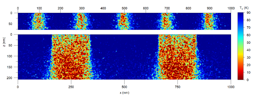
The resulting simulated cross-sectional profiles for the two samples SQ200 and SQ500 are presented in Fig. 2 at the same scale for comparison. Note that sample SQ200 (top panel) was irradiated with a slightly defocused He+ ion beam with approximately Gaussian normal distributed fluence of FWHM = 50 nm, whereas the fluence was homogeneous in the irradiated parts of sample SQ500. Another important difference is the ion energy of 30 keV for sample SQ200 and 75 keV for sample SQ500.
In thin films with nm, 30 keV He+ ion irradiation creates columns, within which is suppressed, that are clearly separated from each other at 200 nm lattice spacing (Fig. 2, top panel). The suppression of at the fringes of the CDs decays more gradually than for sample SQ500, which was irradiated by MIBS (Fig. 2, bottom panel). Still, the cylindrical envelope of clusters with suppressed provides an efficient pinning landscape as will be discussed below.
Due to the larger penetration depth of the 75 keV He+ ions, CDs can be patterned into thicker YBCO films with MIBS, as demonstrated in Fig. 2, bottom panel. However, the achievable lateral resolution for CD diameters degrades with increasing thickness of the film, as it can be noticed by the increasing diameter of the CD for film thicknesses larger than 120 nm. We note that increasing the ion energy would improve the resolution on the cost of a lower ion scattering cross section, which would demand a higher ion fluence.
Although a few dispersed defects are created also outside the CDs by lateral straggling of the incident ions and the secondary collision cascades, their impact on the zero-field electrical transport properties is marginal as demonstrated by the experimentally determined small reduction of the critical temperature K ( K) in sample SQ200 (SQ500) after irradiation.
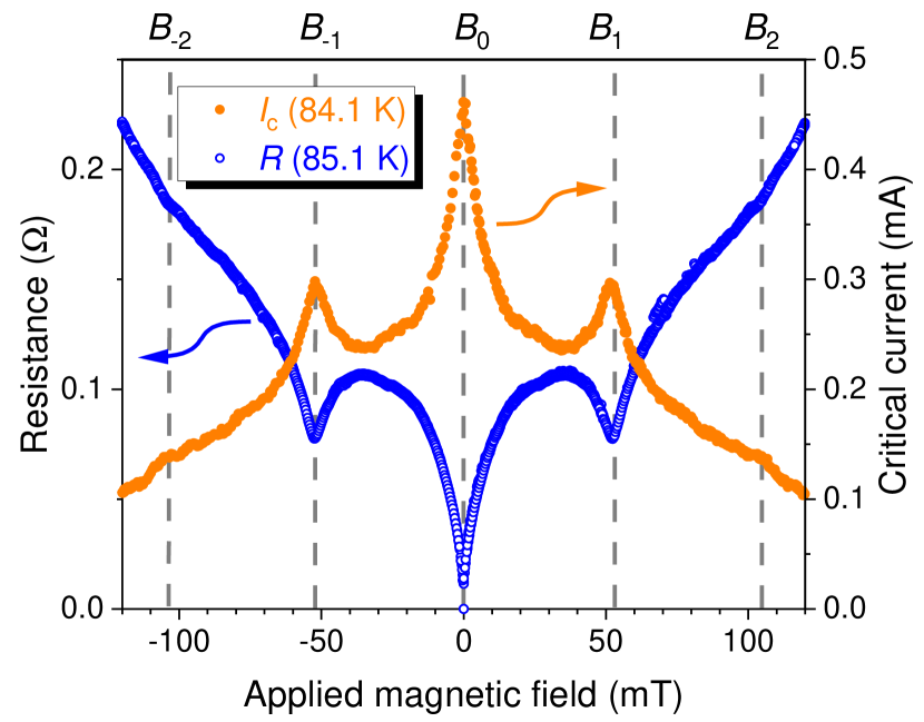
In electric transport measurements, the commensurability effects evoked by regular pinning lattices are demonstrated in Fig. 3 as peaks in the critical current and corresponding minima of the resistance vs applied field (at ) that appear exactly at the matching fields
| (1) |
where is a rational number. We use to denote the absence of vortices and for the reversed vortex orientation. When the diameters of the CDs are larger than the Ginzburg-Landau coherence length, an integer number of fluxons can be accommodated per CD. Buzdin (1993) Note the tiny humps of around mT that indicate a fractional matching pattern with .
The commensurability effects result from two different vortex pinning mechanisms in our samples. On the one hand, flux quanta can be trapped in the normal-conducting core of a CD, which we will call fluxons to discriminate them from the regular Abrikosov vortices in a plain superconductor. These fluxons remain pinned at the CDs even if a moderate current is applied to the sample. However, by changing the applied magnetic field, the Lorentz force due to increased shielding current exceeds the pinning potential and the fluxons can hop between neighboring CDs. Sørensen, Pedersen, and Ögren (2017)
On the other hand, vortices at interstitial positions between the CDs are pinned mainly by twin boundaries and growth defects in the YBCO films, most of them oriented parallel to the axis. Dam et al. (1999) Their pinning potentials are usually weaker than those of the fluxons trapped in the CDs. At a certain applied magnetic field the critical current shows a peak when the magnetic flux through the sample is penetrating the sample via single fluxons trapped in each CD, which happens exactly at the matching field of Eq. 1. In this situation, the number of weakly-pinned interstitial vortices is minimized. An equivalent consideration leads to the explanation of the resistance minima observed at the same . Typically, our samples patterned by masked or focused He+ ion irradiation show clear matching effects in a temperature range from up to .Zechner et al. (2017); Aichner et al. (2019) For our further considerations it is important that the matching fields can be equally well determined from either peaks or resistance minima, the latter allowing for much faster measurements.
An investigation of the angular dependence of the magnetoresistance can shed light on the nature and relative strength of the pinning of fluxons at the CDs and the pinning of interstitial vortices, respectively.
For dominant pinning at CDs the magnetic flux should be preferentially trapped within the CDs irrespectively of the angle by which the applied magnetic field is tilted off the axes of the CDs. Then, the commensurability peaks in and dips in should appear if the component of that is parallel to the axes of the CDs,
| (2) |
fulfills the matching condition of Eq. 1.
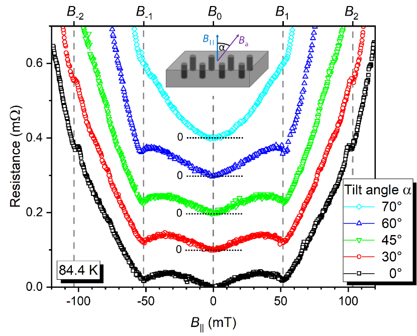
Figure 4 shows the magnetoresistance of sample SQ200 for various tilt angles at a temperature near the onset of dissipation. When the magnetic field is oriented orthogonal to the sample surface and parallel to the axes of the CDs () a distinct minimum at mT and a marginal one at mT confirms the commensurability effects. With increasing tilt angle the magnetoresistance curves exhibit very similar matching resistance minima and change their shapes only slightly if data are plotted with the abscissa scaled to . Even at the commensurability effect can be detected.
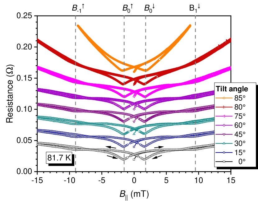
In sample SQ500 the situation is more complicated due to a hysteresis observed in the magnetic field sweeps. It originates from an unconventional terraced critical state Cooley and Grishin (1995) with domains in the sample, Reichhardt et al. (1996) inside which the pinning centers are occupied by the same number of fluxons and neighboring domains by . Such a hysteretic behavior has been investigated previously Zechner et al. (2017) and is beyond the scope of this work. Still, the considerations leading to Eq. 2 should hold. Indeed, Fig. 5 demonstrates that all the features observed in the orientation of appear at the same positions when the magnetic field is tilted and scaling to is used. This not only applies to the first matching fields in upsweep () and downsweep () conditions, but also to the hysteretic displacement of the minima with zero fluxon occupation of the relevant CDs ( and ). Despite of the more complex fluxon arrangements in this sample, all commensurability effects are governed by , which confirms that only the component of the magnetic field is relevant that is parallel to the axes of the CDs.
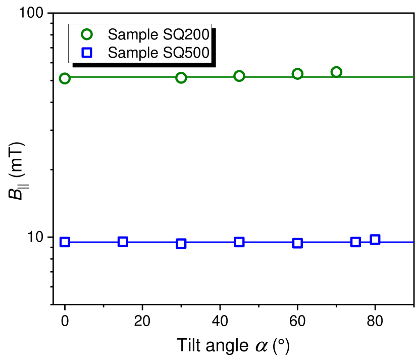
In Fig. 6 the magnetic field components at which the resistance dips for single fluxon matching are observed in sample SQ200 () and SQ500 () are shown as a function of the tilt angle . In remarkable agreement with Eq. (2) the experimental values are independent of as indicated by the horizontal lines. This confirms that at all angles shown in the graph the magnetic flux is penetrated along the CDs. In addition, the adherence to Eq. (2) up to large tilt angles indicates that pinning at the CDs is much stronger than the intrinsic pinning of interstitial vortices in the intermediate regions between the CDs.
Some deviations from the behavior presented in Fig. 6 have been reported in denser pinning lattices. Due to lateral straggling of the collision cascades, a significant number of irradiation defects are created in the spaces between the CDs. This is indicated by K after MIBS irradiation. In this case the scaling according to Eq. 2 gradually breaks down for . Zechner et al. (2018a) In thin YBCO films patterned via 110 keV O+ ion irradiation ( K) a strong modification of the vortex-glass transition and a weakening of the vortex correlations along the axis has been observed. Trastoy et al. (2013)
Finally, in unirradiated YBCO, due to its anisotropy, the cylindrical vortices change to an elliptical cross section in oblique magnetic fields and decompose into a tilted stack of pancake vortices at tilt angles . Blatter et al. (1994) This is reflected by a broad maximum in the critical current extending over a range . Roas, Schultz, and Saemann-Ischenko (1990) The feature evolves at temperatures closer to and in moderate magnetic fields. In contrast to the observations in those unirradiated YBCO films, the matching fields in our samples strictly scale with Eq. (2) up to () for sample SQ200 (SQ500). Naturally, no pinning of fluxons by the CDs is expected when the CDs and are oriented orthogonally, i.e., near .
IV Conclusions
Vortex pinning landscapes in YBCO thin films can be conveniently fabricated by employing He+ ion irradiation, either by a focused beam in a HIM or by shadow-masking of a wide-field ion beam. As demonstrated by simulations of the defect distributions created in YBCO by the ion impact, the methods are complementary. HIM irradiation is a sequential method and allows for maskless operation and higher resolution of at least 10 nm,Müller et al. (2019) but the penetration depth is limited to about 80 nm due to the maximum ion energy of 30 keV. With MIBS the entire pattern can be prepared at the same time and also in thicker films when using higher ion energies, but the lateral resolution is currently limited by a hole diameter of nm of the available stencil masks.
Both methods, despite of their different length scales, produce well-defined CDs that provide strong pinning of fluxons, which is supported by the observation that at arbitrary angles of an applied magnetic field only the component parallel to the CDs governs the commensurability effects. Both irradiation methods appear suitable for the creation of well-defined tailored pinning landscapes in cuprate superconductors, which are an important prerequisite for proposed concepts of fluxon manipulation leading to fast and low-dissipation devices. Wambaugh et al. (1999); Hastings, Olson Reichhardt, and Reichhardt (2003); Milošević, Berdiyorov, and Peeters (2007)
Acknowledgments
Research was conducted within the framework of the COST Action CA16218 (NANOCOHYBRI) of the European Cooperation in Science and Technology. B.M. acknowledges funding by the German Academic Scholarship Foundation. M.D. acknowledges the European Erasmus Mundus (Target II) program for financial support.
References
References
- Kobayashi et al. (1988) N. Kobayashi, H. Iwasaki, S. Terada, K. Noto, A. Tokiwa, M. Kikuchi, Y. Syono, and Y. Muto, “Upper and lower critical fields of REBa2Cu3Oz compounds,” Physica C 153–155, 1525–1526 (1988).
- Clem (1991) J. R. Clem, “Two-dimensional vortices in a stack of thin superconducting films: A model for high-temperature superconducting multilayers,” Phys. Rev. B 43, 7837–7846 (1991).
- Correa et al. (2019) A. Correa, F. Mompeán, I. Guillamón, E. Herrera, M. García-Hernández, T. Yamamoto, T. Kashiwagi, K. Kadowaki, A. I. Buzdin, H. Suderow, and C. Munuera, “Attractive interaction between superconducting vortices in tilted magnetic fields,” Commun. Phys. 2, 31 (2019).
- Haugan et al. (2004) T. Haugan, P. N. Barnes, R. Wheeler, F. Meisenkothen, and M. Sumption, “Addition of nanoparticle dispersions to enhance flux pinning of the YBa2Cu3O7-x superconductor,” Nature 430, 867 (2004).
- Vovk, Khadzhai, and Dobrovolskiy (2019) R. V. Vovk, G. Y. Khadzhai, and O. V. Dobrovolskiy, “Tuning electric charge scattering in YBCO single crystals via irradiation with MeV electrons,” J. Mater. Sci.: Mater. Electron. 30, 241–245 (2019).
- Lang and Pedarnig (2010) W. Lang and J. D. Pedarnig, “Ion irradiation of high-temperature superconductors and its application for nanopatterning,” in Nanoscience and Engineering in Superconductivity, edited by V. V. Moshchalkov, R. Wördenweber, and W. Lang (Springer, Heidelberg, 2010) pp. 81–104.
- Civale (1997) L. Civale, “Vortex pinning and creep in high-temperature superconductors with columnar defects,” Supercond. Sci. Technol. 10, A11–A28 (1997).
- Holzapfel et al. (1993) B. Holzapfel, G. Kreiselmeyer, M. Kraus, S. Bouffard, S. Klaumuenzer, L. Schultz, and G. Saemann-Ischenko, “Angle-resolved critical transport-current density of YBa2Cu3O7-δ thin films and YBa2Cu3O7-δ /PrBa2Cu3O7-δ superlattices containing columnar defects of various orientations,” Phys. Rev. B 48, 600–603 (1993).
- Prozorov et al. (1994) R. Prozorov, A. Tsameret, Y. Yeshurun, G. Koren, M. Konczykowski, and S. Bouffard, “Angular dependence of the magnetic properties of thin YBa2Cu3O7-δ films irradiated with Pb and Xe ions,” Physica C 234, 311 – 317 (1994).
- Silhanek, Civale, and Avila (2002) A. V. Silhanek, L. Civale, and M. A. Avila, “Columnar defects acting as passive internal field detectors,” Phys. Rev. B 65, 174525 (2002).
- Roas, Schultz, and Saemann-Ischenko (1990) B. Roas, L. Schultz, and G. Saemann-Ischenko, “Anisotropy of the critical current-density in epitaxial YBa2Cu3Ox films,” Phys. Rev. Lett. 64, 479–482 (1990).
- Sekirnjak et al. (1995) C. Sekirnjak, W. Lang, S. Proyer, and P. Schwab, “Novel approach for the analysis of the fluctuation magnetoconductivity in YBa2Cu3O7 thin films,” Physica C 243, 60–68 (1995).
- Fiory, Hebard, and Somekh (1978) A. T. Fiory, A. F. Hebard, and S. Somekh, “Critical currents associated with the interaction of commensurate flux-line sublattices in a perforated Al film,” Appl. Phys. Lett. 32, 73–75 (1978).
- Lykov (1993) A. N. Lykov, “Pinning in superconducting films with triangular lattice of holes,” Solid State Commun. 86, 531–533 (1993).
- Metlushko et al. (1994) V. V. Metlushko, M. Baert, R. Jonckheere, V. V. Moshchalkov, and Y. Bruynseraede, “Matching effects in Pb/Ge multilayers with the lattice of submicron holes,” Solid State Commun. 91, 331–335 (1994).
- Metlushko et al. (1998) V. V. Metlushko, L. E. DeLong, M. Baert, E. Rosseel, M. J. Van Bael, K. Temst, V. V. Moshchalkov, and Y. Bruynseraede, “Supermatching vortex phases in superconducting thin films with antidot lattices,” Europhys. Lett. 41, 333–338 (1998).
- Kemmler et al. (2006) M. Kemmler, C. Gürlich, A. Sterck, H. Pöhler, M. Neuhaus, M. Siegel, R. Kleiner, and D. Koelle, “Commensurability effects in superconducting Nb films with quasiperiodic pinning arrays,” Phys. Rev. Lett. 97, 147003 (2006).
- Misko et al. (2010) V. R. Misko, D. Bothner, M. Kemmler, R. Kleiner, D. Koelle, F. M. Peeters, and F. Nori, “Enhancing the critical current in quasiperiodic pinning arrays below and above the matching magnetic flux,” Phys. Rev. B 82, 184512 (2010).
- Moshchalkov and Fritzsche (2011) V. V. Moshchalkov and J. Fritzsche, Nanostructured superconductors (World Scientific, Singapore, 2011).
- Vélez et al. (2008) M. Vélez, J. I. Martín, J. E. Villegas, A. Hoffmann, E. M. González, J. L. Vicent, and I. K. Schuller, “Superconducting vortex pinning with artificial magnetic nanostructures,” J. Magn. Magn. Mater. 320, 2547–2562 (2008), and references therein.
- Shklovskij and Dobrovolskiy (2006) V. A. Shklovskij and O. V. Dobrovolskiy, “Influence of pointlike disorder on the guiding of vortices and the Hall effect in a washboard planar pinning potential,” Phys. Rev. B 74, 104511 (2006).
- Shklovskij and Dobrovolskiy (2008) V. A. Shklovskij and O. V. Dobrovolskiy, “ac-driven vortices and the Hall effect in a superconductor with a tilted washboard pinning potential,” Phys. Rev. B 78, 104526 (2008).
- Dobrovolskiy et al. (2012) O. V. Dobrovolskiy, E. Begun, M. Huth, and V. A. Shklovskij, “Electrical transport and pinning properties of Nb thin films patterned with focused ion beam-milled washboard nanostructures,” New J. Phys. 14, 113027 (2012).
- Dobrovolskiy et al. (2018) O. V. Dobrovolskiy, V. M. Bevz, M. Y. Mikhailov, O. L. Yuzephovich, V. A. Shklovskij, R. V. Vovk, M. I. Tsindlekht, R. Sachser, and M. Huth, “Microwave emission from superconducting vortices in Mo/Si superlattices,” Nat. Commun. 9, 4927 (2018).
- Castellanos et al. (1997) A. Castellanos, R. Wördenweber, G. Ockenfuss, A. v.d. Hart, and K. Keck, “Preparation of regular arrays of antidots in YBa2Cu3O7 thin films and observation of vortex lattice matching effects,” Appl. Phys. Lett. 71, 962–964 (1997).
- Wang et al. (1995) X. Z. Wang, B. Hellebrand, D. Bäuerle, M. Strecker, G. Wortmann, and W. Lang, “Oxygen ordering and superconductivity in GdBaSrCu3O7-x,” Physica C 242, 55–62 (1995).
- Sefrioui et al. (2001) Z. Sefrioui, D. Arias, E. M. González, C. Léon, J. Santamaria, and J. L. Vicent, “Vortex liquid entanglement in irradiated YBa2Cu3O7-δ thin films,” Phys. Rev. B 63, 064503 (2001).
- Lang et al. (2004) W. Lang, T. Enzenhofer, M. Peruzzi, J. D. Pedarnig, D. Bäuerle, C. Horner, E. Cekan, E. Platzgummer, and H. Loeschner, “Tailoring the transport properties of YBa2Cu3O7-δ thin films by light-ion irradiation,” Inst. Phys. Conf. Ser. 181, 1549–1555 (2004).
- Cybart et al. (2014) S. A. Cybart, P. X. T. Yen, E. Y. Cho, J. U. Huh, V. N. Glyantsev, C. S. Yung, B. Moeckly, J. W. Beeman, and R. C. Dynes, “Comparison of Y–Ba–Cu–O films irradiated with helium and neon ions for the fabrication of Josephson devices,” IEEE Trans. Appl. Supercond. 24, 1–5 (2014).
- Lang et al. (2006) W. Lang, M. Dineva, M. Marksteiner, T. Enzenhofer, K. Siraj, M. Peruzzi, J. D. Pedarnig, D. Bäuerle, R. Korntner, E. Cekan, E. Platzgummer, and H. Loeschner, “Ion-beam direct-structuring of high-temperature superconductors,” Microelectron. Eng. 83, 1495–1498 (2006).
- Lang et al. (2009) W. Lang, H. Richter, M. Marksteiner, K. Siraj, M. A. Bodea, J. D. Pedarnig, C. Grigoropoulos, D. Bäuerle, C. Hasenfuss, L. Palmetshofer, R. Kolarova, and P. Bauer, “Masked ion beam irradiation of high-temperature superconductors: patterning of nano-size regions with high point-defect density,” Int. J. Nanotechnol. 6, 704–14 (2009).
- Pedarnig et al. (2010) J. D. Pedarnig, K. Siraj, M. A. Bodea, I. Puica, W. Lang, R. Kolarova, P. Bauer, K. Haselgrübler, C. Hasenfuss, I. Beinik, and C. Teichert, “Surface planarization and masked ion-beam structuring of YBa2Cu3O7 thin films,” Thin Solid Films 518, 7075–80 (2010).
- Swiecicki et al. (2012) I. Swiecicki, C. Ulysse, T. Wolf, R. Bernard, N. Bergeal, J. Briatico, G. Faini, J. Lesueur, and J. E. Villegas, “Strong field-matching effects in superconducting YBa2Cu3O7-δ films with vortex energy landscapes engineered via masked ion irradiation,” Phys. Rev. B 85, 224502 (2012).
- Trastoy et al. (2013) J. Trastoy, V. Rouco, C. Ulysse, R. Bernard, A. Palau, T. Puig, G. Faini, J. Lesueur, J. Briatico, and J. E. Villegas, “Unusual magneto-transport of YBa2Cu3O7-δ films due to the interplay of anisotropy, random disorder and nanoscale periodic pinning,” New J. Phys. 15, 103022 (2013).
- Haag et al. (2014) L. T. Haag, G. Zechner, W. Lang, M. Dosmailov, M. A. Bodea, and J. D. Pedarnig, “Strong vortex matching effects in YBCO films with periodic modulations of the superconducting order parameter fabricated by masked ion irradiation,” Physica C 503, 75–81 (2014).
- Zechner et al. (2017) G. Zechner, F. Jausner, L. T. Haag, W. Lang, M. Dosmailov, M. A. Bodea, and J. D. Pedarnig, “Hysteretic vortex-matching effects in high- superconductors with nanoscale periodic pinning landscapes fabricated by He ion-beam projection,” Phys. Rev. Applied 8, 014021 (2017).
- Zechner et al. (2018a) G. Zechner, K. L. Mletschnig, W. Lang, M. Dosmailov, M. A. Bodea, and J. D. Pedarnig, “Unconventional critical state in YBa2Cu3O7-δ thin films with a vortex-pin lattice fabricated by masked He+ ion beam irradiation,” Supercond. Sci. Technol. 31, 044002 (2018a).
- Zechner et al. (2018b) G. Zechner, W. Lang, M. Dosmailov, M. A. Bodea, and J. D. Pedarnig, “Transverse vortex commensurability effect and sign change of the Hall voltage in superconducting YBa2Cu3O7-δ thin films with a nanoscale periodic pinning landscape,” Phys. Rev. B 98, 104508 (2018b).
- Aichner et al. (2019) B. Aichner, B. Müller, M. Karrer, V. R. Misko, F. Limberger, K. L. Mletschnig, M. Dosmailov, J. D. Pedarnig, F. Nori, R. Kleiner, D. Koelle, and W. Lang, “Ultradense tailored vortex pinning arrays in superconducting YBa2Cu3O7-δ thin films created by focused He ion beam irradiation for fluxonics applications,” ACS Appl. Nano Mater. 2, 5108–5115 (2019).
- Womack et al. (2019) F. N. Womack, P. W. Adams, J. M. Valles, and G. Catelani, “Critical field behavior of a multiply connected superconductor in a tilted magnetic field,” Phys. Rev. B 100, 174505 (2019).
- Emmrich et al. (2016) D. Emmrich, A. Beyer, A. Nadzeyka, S. Bauerdick, J. C. Meyer, J. Kotakoski, and A. Gölzhäuser, “Nanopore fabrication and characterization by helium ion microscopy,” Appl. Phys. Lett. 108, 163103 (2016).
- Heine and Lang (1998) G. Heine and W. Lang, “Magnetoresistance of the new ceramic ‘Cernox’ thermometer from 4.2 K to 300 K in magnetic fields up to 13 T,” Cryogenics 38, 377–379 (1998).
- Ziegler, Littmark, and Biersack (1985) J. F. Ziegler, U. Littmark, and J. P. Biersack, The stopping and range of ions in solids (Pergamon, New York, 1985).
- Ziegler, Ziegler, and Biersack (2010) J. F. Ziegler, M. D. Ziegler, and J. P. Biersack, “SRIM – the stopping and range of ions in matter (2010),” Nucl. Instrum. Methods Phys. Res., Sect. B 268, 1818–23 (2010).
- Müller et al. (2019) B. Müller, M. Karrer, F. Limberger, M. Becker, B. Schröppel, C. J. Burkhardt, R. Kleiner, E. Goldobin, and D. Koelle, “Josephson junctions and squids created by focused helium-ion-beam irradiation of ,” Phys. Rev. Applied 11, 044082 (2019).
- Abrikosov and Gor’kov (1960) A. A. Abrikosov and L. P. Gor’kov, “Contribution to the theory of superconducting alloys with paramagnetic impurities,” Zh. Eksp. Teor. Fiz. 39, 1781 (1960), Sov. Phys. JETP 12, 1243 (1961).
- Mletschnig and Lang (2019) K. L. Mletschnig and W. Lang, “Nano-patterning of cuprate superconductors by masked He+ ion irradiation: 3-dimensional profiles of the local critical temperature,” Microelectron. Eng. 215, 110982 (2019).
- Buzdin (1993) A. I. Buzdin, “Multiple-quanta vortices at columnar defects,” Phys. Rev. B 47, 11416 (1993).
- Sørensen, Pedersen, and Ögren (2017) M. P. Sørensen, N. F. Pedersen, and M. Ögren, “The dynamics of magnetic vortices in type II superconductors with pinning sites studied by the time dependent Ginzburg–Landau model,” Physica C 533, 40–43 (2017).
- Dam et al. (1999) B. Dam, J. M. Huijbregtse, F. C. Klaassen, R. C. F. van-der Geest, G. Doornbos, J. H. Rector, A. M. Testa, S. Freisem, J. C. Martinez, B. Stäuble-Pümpin, and R. Griessen, “Origin of high critical currents in YBa2Cu3O7-δ superconducting thin films,” Nature 399, 439–442 (1999).
- Cooley and Grishin (1995) L. D. Cooley and A. M. Grishin, “Pinch effect in commensurate vortex-pin lattices,” Phys. Rev. Lett. 74, 2788–2791 (1995).
- Reichhardt et al. (1996) C. Reichhardt, J. Groth, C. J. Olson, S. B. Field, and F. Nori, “Spatiotemporal dynamics and plastic flow of vortices in superconductors with periodic arrays of pinning sites,” Phys. Rev. B 54, 16108 (1996), Erratum: Phys. Rev. B 56, 14196 (1997).
- Blatter et al. (1994) G. Blatter, M. Feigel’man, V. Geshkenbein, A. Larkin, and V. Vinokur, “Vortices in high-temperature superconductors,” Rev. Mod. Phys. 66, 1125–1388 (1994).
- Wambaugh et al. (1999) J. F. Wambaugh, C. Reichhardt, C. J. Olson, F. Marchesoni, and F. Nori, “Superconducting fluxon pumps and lenses,” Phys. Rev. Lett. 83, 5106–5109 (1999).
- Hastings, Olson Reichhardt, and Reichhardt (2003) M. B. Hastings, C. J. Olson Reichhardt, and C. Reichhardt, “Ratchet cellular automata,” Phys. Rev. Lett. 90, 247004 (2003).
- Milošević, Berdiyorov, and Peeters (2007) M. V. Milošević, G. R. Berdiyorov, and F. M. Peeters, “Fluxonic cellular automata,” Appl. Phys. Lett. 91, 212501 (2007).