Dual Topological Insulator Device with Disorder Robustness
Abstract
Two-dimensional \chNa3Bi is a dual topological insulator protected by time-reversal and mirror symmetry, resulting in a promising platform for devices design. However, in reality, the design of topological devices is hindered by a sensitivity against disorder and temperature. We study the topological properties of \chNa3Bi in the presence of intrinsic defects, investigating the robustness of the edge states and the resulting transport properties. We apply a recursive Green’s function technique enabling the study of disordered systems with lengths comparable to experimentally synthesized materials, in the order of micrometers. We combine our findings to propose a topological insulator device, where intrinsic defects are used to filter the response of trivial bulk states. This results in a stable conductance throughout a large range of electronic temperatures, and controllable by a perpendicular electric field. Our proposal is general, enabling the design of various dual topological insulators devices.
I Introduction
Kane and Mele (2005a) showed that the spin-orbit interaction plays a key role in the topology of the electronic structure of a graphene lattice, realizing the quantum spin Hall (QSH) state that is characterized by a topological invariant Kane and Mele (2005b). Distinguished by the non-zero invariant, quantum spin Hall insulators (QSHIs) feature counter-propagating helical gapless states localized at the boundary with a trivial insulator Hasan and Kane (2010); Qi and Zhang (2011); Ando (2013); Bansil et al. (2016). These edge (surface) states are robust against elastic backscattering due to the bulk electronic structure protected by time-reversal symmetry (TRS) Hasan and Kane (2010); Qi and Zhang (2011); Ando (2013); Bansil et al. (2016) and the bulk boundary equivalence Fukui et al. (2012). The presence of metallic edge states is mainly characterized by angle-resolved photoemission spectroscopy (ARPES), probing the electronic structure at the edges (surfaces) of a 2D (3D) QSHI König et al. (2007); Bernevig et al. (2006). To date, there are few QSHIs experimentally realized and several theoretically proposed König et al. (2007); Knez et al. (2011); Qian et al. (2014); Reis et al. (2017); Costa et al. (2019); Schleder et al. (2019); Olsen et al. (2019); Marrazzo et al. (2019), but their characterization and application is often limited by the size of the bandgap, which is usually small Ando (2013); Bansil et al. (2016).
Besides TRS, crystalline symmetries may also protect a distinct topological character, resulting in topological crystalline insulators (TCIs) Fu (2011); Ando and Fu (2015). The TCI state is more commonly found to be protected by mirror symmetries, and also results in dissipationless states at the boundary with a trivial insulator. Mirror protected TCIs are characterized by a non-zero mirror Chern number () Teo et al. (2008). Several other symmetries may protect the bulk topology resulting in different topological insulators (TIs) Benalcazar et al. (2017); Schindler et al. (2018); Cayssol et al. (2013); Kawabata et al. (2019), a particular and yet less explored case is the dual topological insulator (DTI), when the bulk topology is simultaneously protected by TR and crystal symmetries Teo et al. (2008); Weber et al. (2015); Eschbach et al. (2016). For QSHIs (TCIs), breaking TR (crystalline) symmetry would result in a trivial insulator. As a DTI, breaking time-reversal (mirror) symmetry alone would still result in gapless edge states protected by the mirror (time-reversal) symmetry, allowing us to separately control both topological phases Acosta and Fazzio (2019).
Na3Bi is a DTI among those with the largest bandgap, additionally, it also possesses a robust band inversion and great stability under strain Niu et al. (2017). Recently, an electrical driven quantum phase transition was experimentally observed Collins et al. (2018), turning \chNa3Bi in a promising candidate to be applicable on TI devices. The experimental realization of \chNa3Bi and its characterization revealed the presence of spontaneous occurring defects at step edges that could alter the material properties in the application Collins et al. (2018). However, the investigation of the electronic structure and transport properties of defective DTIs is unexplored in the literature.
We study \chNa3Bi defects at the edges of armchair nanoribbons. We employ density functional theory (DFT) Hohenberg and Kohn (1964); Kohn and Sham (1965) for geometry optimization and electronic structure calculations, obtaining the ab initio Hamiltonians for transport calculations. We make use of the non-equilibrium Green’s function (NEGF)Datta (1995); Caroli et al. (1971); Xue et al. (2002); Brandbyge et al. (2002); Sanvito et al. (1999); Nardelli (1999) method to account for transport properties and using a recursive scheme we study the effect of disorder on \chNa3Bi with ribbon lengths up to . Inspired by the electric field topological phase transition, we propose the use of disordered \chNa3Bi to compose a device that is highly controllable and stable at high electronic temperatures.
II Methods
II.1 Electronic structure
Bulk electronic structure calculations shown in Fig. 2 were performed with VASP Kresse and Furthmüller (1996, 1996) using the projector augmented-wave (PAW) method Kresse and Joubert (1999) and self-consistent spin-orbit coupling (SOC). The kinetic energy cutoff for the plane wave expansion was , with k-point density of 20 .
Nanoribbons electronic structures and defects relaxations, shown in Fig. 3, were performed with the SIESTA Soler et al. (2002) code using an optimized polarized single- (SZP) basis-set, which is sufficient to replicate the plane-waves band structure with satisfactory accuracy. The geometry optimization procedure for the considered defects was performed until the Hellmann-Feynman forces were smaller than . The electronic structure calculations were performed with the on-site self-consistent SOC Fernández-Seivane et al. (2006); Fernández-Seivane and Ferrer (2007) as well as fully-relativistic norm-conserving pseudopotentials Troullier and Martins (1991) and energy grid cut-off of 350 Ry. As for k-space sampling, we used a k-point density larger than 16 . We added of vacuum to avoid spurious interactions between periodic images in non-periodic directions. We passivated the ribbons’ edges with hydrogen to circumvent dangling bonds effects. Furthermore, the pristine leads are modeled as one unit-cell armchair nanoribbons with in length, and the scattering region as four unit-cell armchair nanoribbons with in length. All nanoribbons are wide, which is sufficient to present gapless edge states.
II.2 Ballistic transport
The transport coefficients were obtained using the system’s setup with left (L) and right (R) semi-infinite leads with a scattering region (S) in between, see Fig. 1(a). In the small bias regime and at , the conductance through the scattering region can be expressed by the Landauer formula Büttiker et al. (1985), where is the transmission at the Fermi level. The transmission is written in terms of the Green’s function of the scattering region and the coupling matrices between the scattering region and the leads as in Eq. (1) Caroli et al. (1971); Meir and Wingreen (1992). To compute the scattering region Green’s function and the leads coupling matrices we implemented the method described by ref. Sanvito et al. (1999); Rocha et al. (2006, 2010a) using the self-consistent converged DFT Hamiltonians obtained directly from SIESTA.
| (1) |
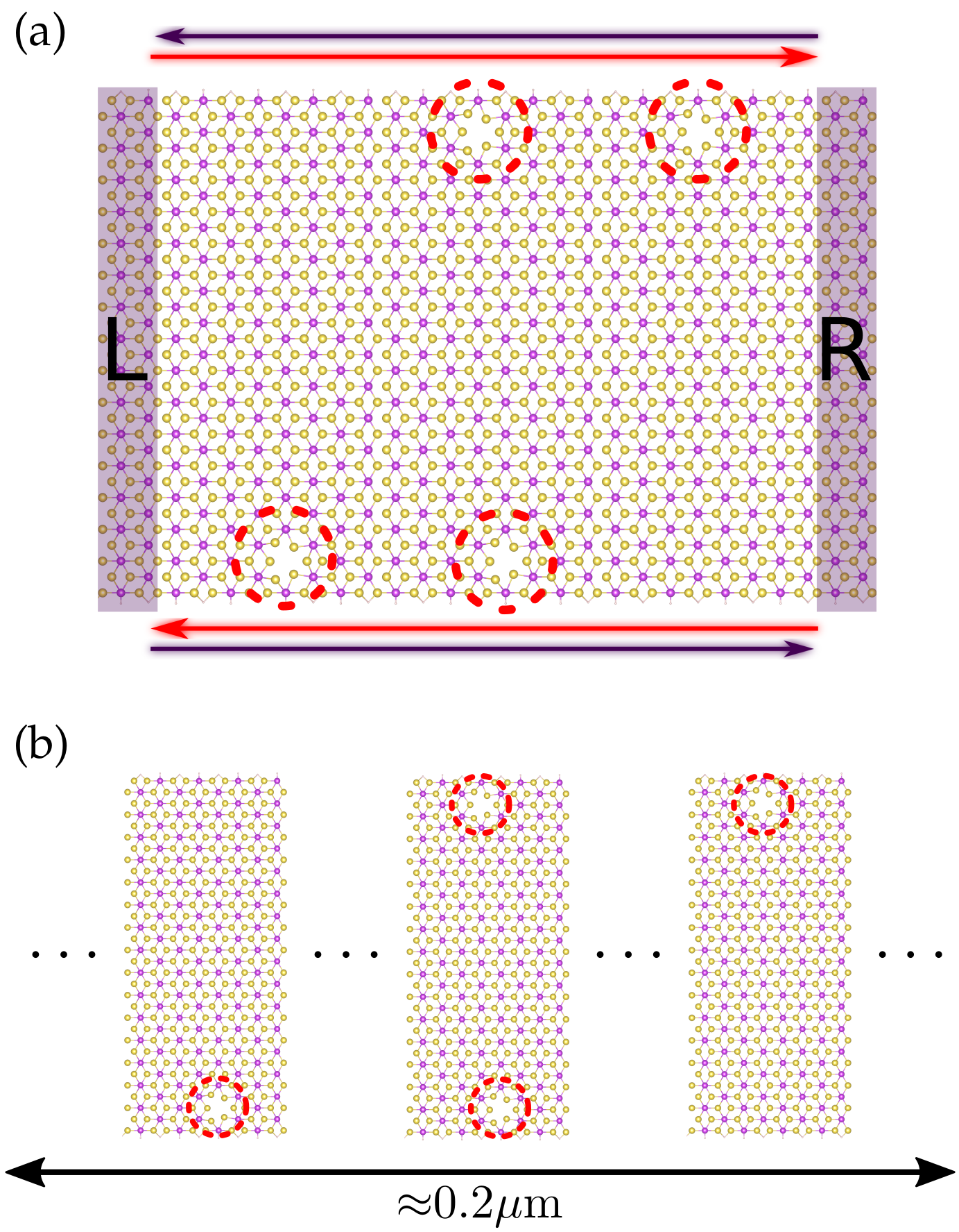
The method itself does not limit the size of the scattering region, the main difficulty arises in the calculation of the Green’s function using an ab initio Hamiltonian, which may be challenging regarding the system’s size and the basis set used in the calculation. To achieve real length scattering regions and to enable the study of disordered systems we must combine the NEGF method with the recursive Green’s function technique Sanvito et al. (1999); Rocha et al. (2010a); Lewenkopf and Mucciolo (2013); Markussen et al. (2006). The recursive procedure starts by splitting the total scattering region into building blocks in such a way that each building block has an isolated defect, as illustrated in Fig. 1(b). The blocks are connected via first neighbors’ interactions. This division of the scattering region allows us to compute the ab initio DFT Hamiltonian and overlap matrix for each building block separately and use the method to recursively eliminate internal degrees of freedom of the scattering region Hamiltonian. The result is an effective Hamiltonian describing the whole scattering region. The computational cost of using this technique to compute the system’s transport coefficients is similar to the computational cost of calculating the Green’s function of a single building block. As such, the recursive method has already been successfully applied to study several large length systems, reaching scales up to hundreds of nanometers Rocha et al. (2010a); Lewenkopf and Mucciolo (2013); Markussen et al. (2006); Rocha et al. (2008, 2010b); de Almeida et al. (2011); Pezo et al. (2019).
III Results and Discussion
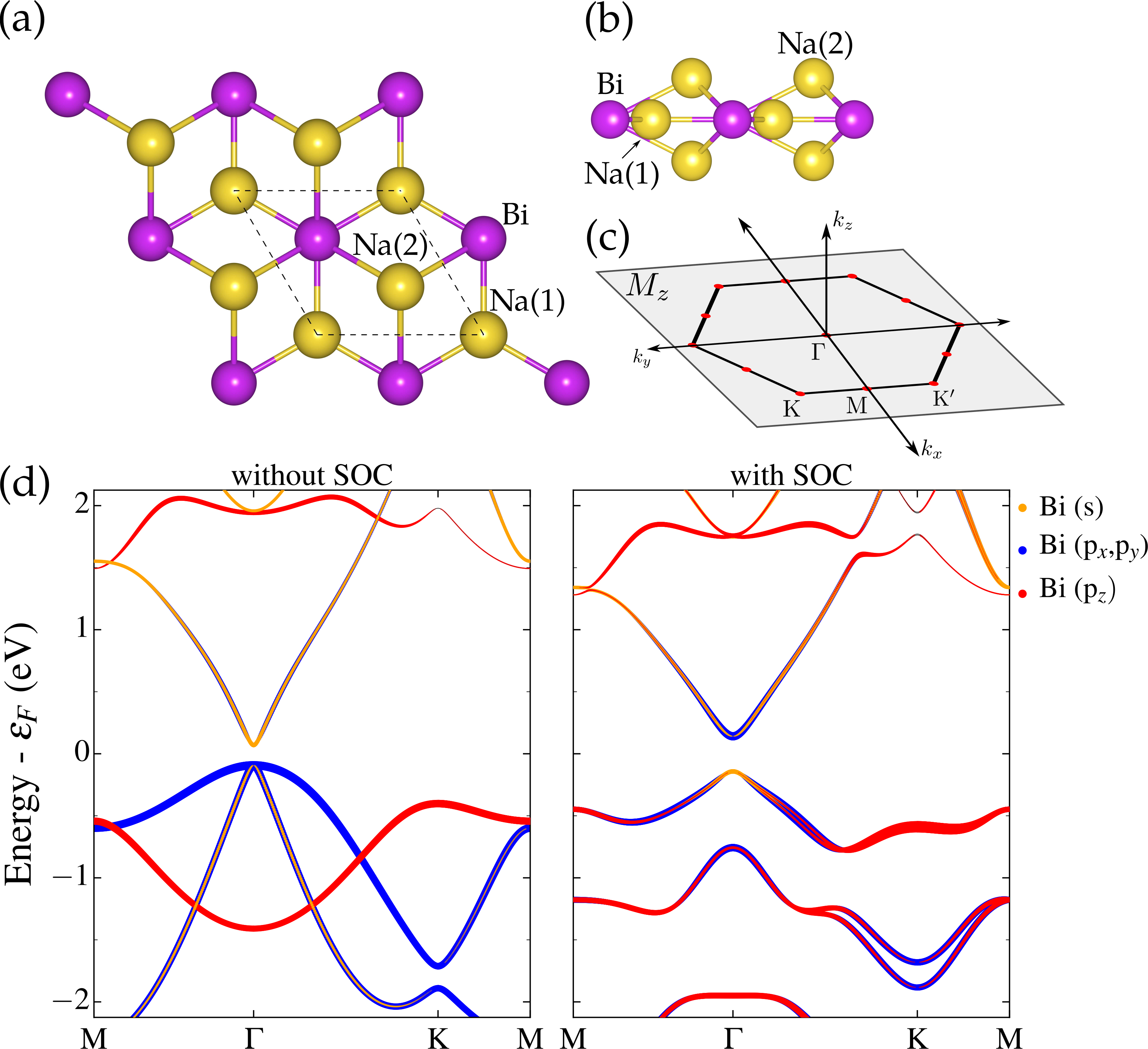
Our starting reference is bulk \chNa3Bi, with its two-dimensional atomic arrangement depicted in Fig. 2. Sodium atoms have two distinct positions, Na(1) as in-plane atoms and Na(2) as out-of-plane atoms. \chNa3Bi forms a honeycomb lattice preserving three-fold rotation about the z-axis as shown in Fig. 2(a). Besides symmetry, there is a mirror-symmetric plane perpendicular to the z-axis (), as illustrated in Fig. 2(b)–(c), that plays a key role in the topology of \chNa3Bi electronic structure. The 3D counterpart of \chNa3Bi is composed of stacked monolayers and is a topological Dirac semimetal (TDS) Liu et al. (2014), in contrast, 2D \chNa3Bi is an insulator Niu et al. (2017). Figure 2(d) shows its band structure with and without spin-orbit coupling (SOC). Without SOC, the bandgap is located at , with the valence band (VB) and conduction band (CB) mainly composed of Bi- orbitals with a small contribution of Bi- orbital at the CB minimum (CBM). With SOC, there is a band inversion at , with the VB mainly composed of Bi- with a larger contribution of Bi- at the VB maximum (VBM), and the CBM switches to mainly Bi- orbitals. The bandgap with SOC is and it remains direct at , in agreement with previous results Niu et al. (2017); Collins et al. (2018). \chNa3Bi is a well known DTI, with its dual topological character due to time-reversal and crystalline symmetry Niu et al. (2017); Collins et al. (2018). We verified \chNa3Bi topology computing the and topological invariants Soluyanov and Vanderbilt (2011); Gresch et al. (2017); Teo et al. (2008), which resulted in and , respectively.
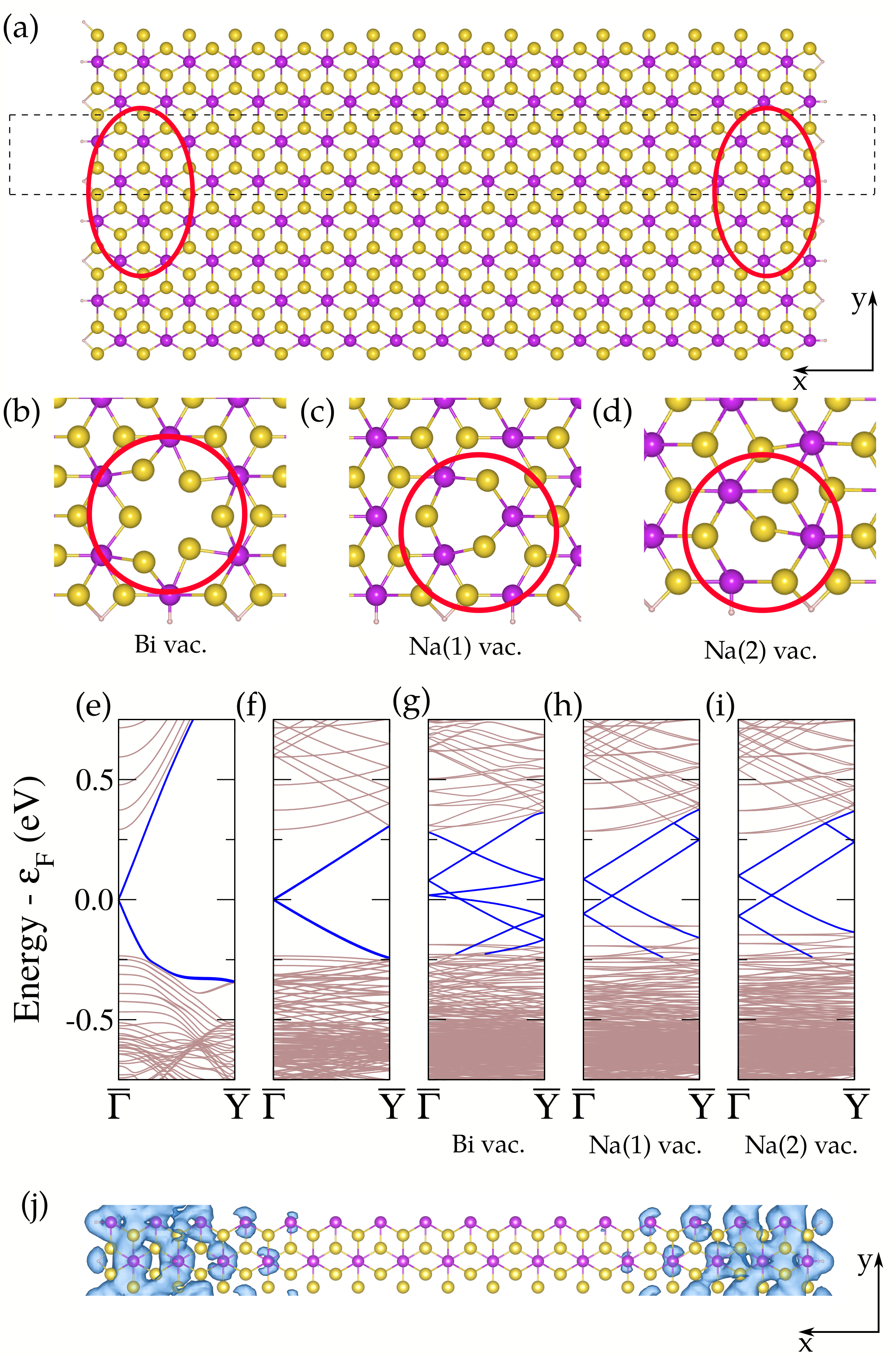
The interface between topological and trivial insulators carries gapless states that are robust to disorder as long as the bulk boundary correspondence holds and the edge preserves the same symmetry that protects the bulk topology Fukui et al. (2012). To access such robustness we study intrinsic defects near \chNa3Bi edges. First, we compute the band structure (Fig. 3(e)) of a \chNa3Bi armchair nanoribbon shown in Fig. 3(a). The ribbon band structure clearly shows gapless states inside the bulk bandgap, and in Fig. 3(j) the charge density plot verifies that these states are spatially located at the ribbon’s edges. We repeated the unit-cell armchair ribbon along the periodic direction to create a four-unit-cell ribbon to be used as a platform for defect calculations. The geometry and band structure are seen in Fig. 3(a) and 3(f), respectively. Next, we place vacancies close to the edges of these ribbons (positions marked in red in Fig. 3(a)).
Na(2) vacancies with formation energy of should be much more common than both Na(1) and Bi vacancies, with formation energies of and , respectively. As observed in experiments Collins et al. (2018), Na(2) vacancies are expected to appear at the edges. With a Bi vacancy, Fig. 3(g), the dispersion of the edge state is decreased, but remains linear near with the bandgap closed and the folded topological states emerging from the bulk bands. The edge states of Na(1) and Na(2) defects (Fig. 3(h) and 3(i), respectively) affect only the defective edge also breaking edge degeneracy. We observe non-topological defect-like localized states inside the gap near the valence band which intersects the edge states.
The presence of these defects locally breaks the mirror symmetry as a result of relaxation, for Na(1) and Bi defects, and also by the missing atomic position for Na(2) defects. There is no net magnetic moment resulting from these defects, preserving TRS. The presence of defects on TIs can cause interference on edge states as a result of small ribbon widths Vannucci et al. (2020) or high vacancy concentration Tiwari et al. (2019), where the defects mediate the coupling between the states on opposite edges leading to backscattering. The ribbons used in our calculations are almost wide, therefore, the defects studied at concentrations of about are not enough to disturb the correspondence with the bulk and they do not interfere with the topological states, remaining with a closed bandgap. In the following, we show that edge defects besides preserving topological states, are also beneficial for transport properties.
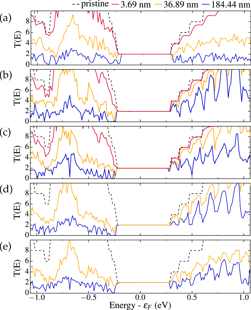
To access the robustness of \chNa3Bi against disorder we compute the total electronic transmission of the nanoribbons through the recursive technique considering different degrees of disorder. In Fig. 4 we consider mixed defects on either and both edges, starting from a single defect () until reaching a scattering region with . Figure 4(a) demonstrates the effect of Bi defects solely. Bulk states are localized by the defects resulting in the decrease of transmission as the ribbon length increases, however, the edge states are little affected by the presence of defects and the transmission remains quantized at the bandgap even with long ribbon lengths. Figure 4(b)–(d) shows the transmission for Na defects. Na(1) and Na(2) (see Fig. 4(b) and 4(c), respectively) defects do not change the transmission of the states inside the gap, although they hinder the bulk transmission. Mixing Na(1) and Na(2) defects (see Fig. 4(d)) shows the same trend, increasing the ribbon length only modifies the bulk transmission. Also, as seen in Fig. 4(e), adding Bi defects to the scattering region has a greater localization effect for bulk trivial states than Na defects alone.
Figure 4 provides an insight into the robustness of the edge states of a topological insulator under structural disorder. Even with defects that locally break the mirror symmetry, the topological states proved to be highly robust. The recent realization of an amorphous TI Costa et al. (2019) proved that topological states may be persistent in strong structural disorder regimes. In SiC supported bismuthene, the topological states resist a random vacancy concentration threshold of almost Ni et al. (2020), with this value dependent on the material’s band gap and SOC strength Ni et al. (2020); Tiwari et al. (2019). In \chNa3Bi, with vacancy concentration up to , the transmission (conductance) of the topological edge states take a constant value of 2 (G0) resulting from the edge states dispersion even in length scales of micrometers. Figure 4 clearly shows that bulk states transmission are vanishingly small in real length scattering regions, therefore, enabling the construction of devices where defects are desirable, allowing the filtering of bulk states while retaining only the response of topological states.
Topological insulators devices should possess two main features allowing their application: controllability, with the switch between on and off states, and thermal stability. \chNa3Bi has a topological phase transition induced by a perpendicular electric field, as displayed in Fig. 5(a). The on and off switch is performed by the conductance having a value of and zero, respectively, see Fig. 5(b). Electronic and structural temperature effects can give rise to the contribution of bulk states to the conductance, resulting in a higher conductance and reducing the device’s controllability Wu et al. (2018), as displayed in Fig. 5(b).
Using the effect caused by defects, we propose a TI device controllable through a topological phase transition, and with electronic thermal stability at high electronic temperatures, see Fig. 5(c). The main feature here is the use of defects to filter the bulk states stabilizing the response of the device. We investigate the phase transition produced by an electric field, that is a result of breaking the mirror symmetry, and also the Stark effect that rearranges the bands orbital character Collins et al. (2018). The control of topological states through the application of an electric field has been proposed in several works Niu et al. (2017); Qian et al. (2014); Liu et al. (2015), but the consequences in transport properties in disordered TIs, and DTIs, and the effect of electronic temperature in these systems still lacks a proper investigation.
| (2) |
where the derivative of the Fermi-Dirac distribution is the thermal broadening function accounting for electronic temperature effects in the conductance.
In Fig. 5(b), we evaluate Eq. (2) as a function of the temperature, as given by the derivative of the Fermi-Dirac distribution, for four different configurations: (i) pristine \chNa3Bi, (ii) pristine \chNa3Bi with a perpendicular electric field applied, (iii) disordered \chNa3Bi with no applied electric field and (iv) disordered \chNa3Bi with a perpendicular electric field applied ().
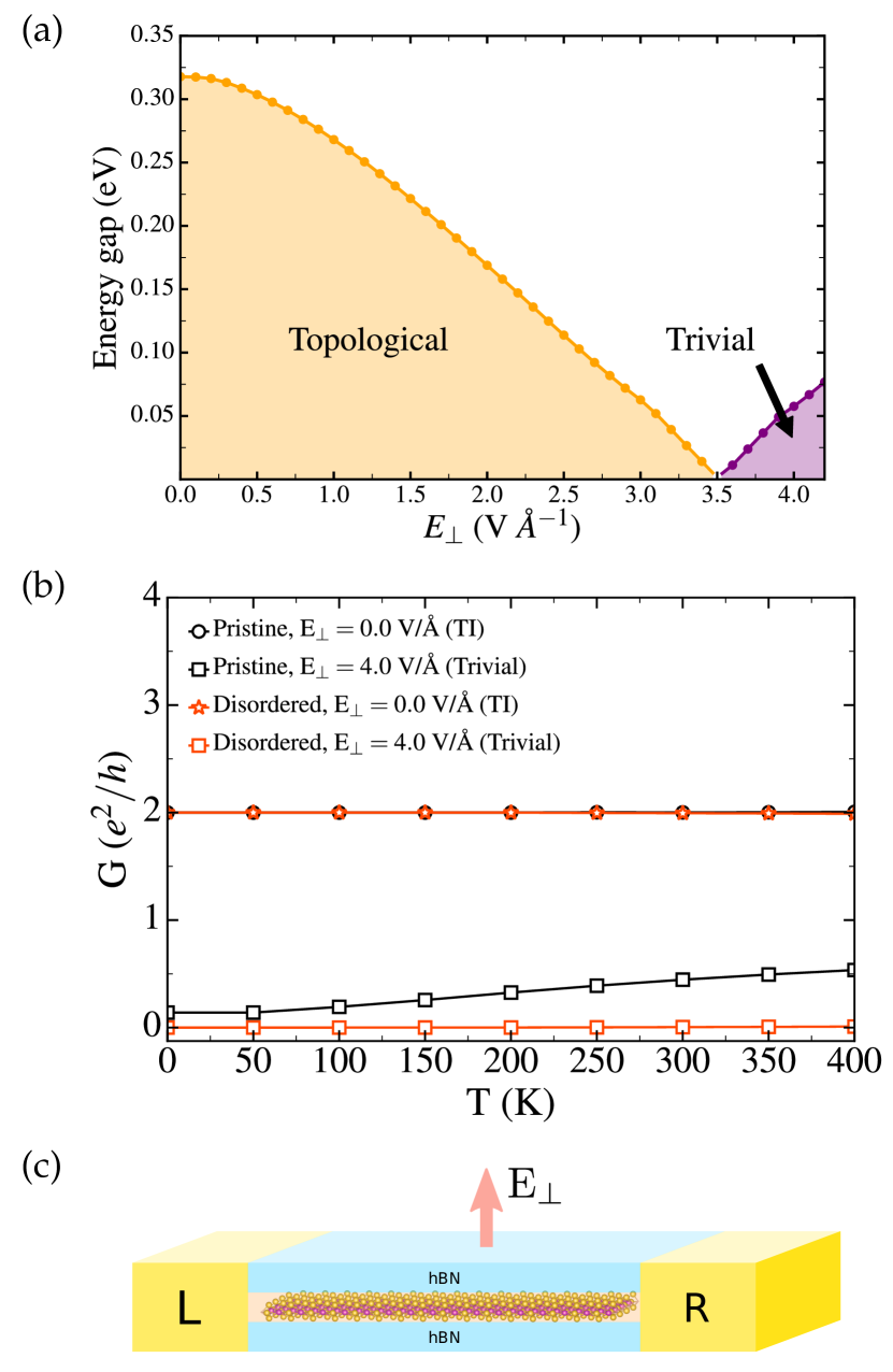
The large band gap in \chNa3Bi ensures a quantized conductance for medium temperatures, regardless of the presence of structural disorder. However, with the applied electric field, as the electronic temperature increases, pristine \chNa3Bi shows an increase in conductance due to tunneling between states of the valence and conduction bands, harming the on/off ratio, and therefore the controllability. The same is not observed for disordered \chNa3Bi, the conductance vanishes with the application of a perpendicular electric field in the disordered regime; the conductance is close to zero even at high temperatures, resulting in a thermally stable response. Even though we only include electronic temperature effects, \chNa3Bi has shown to be highly stable against strain up to 20% change in the lattice parameter without closing the band gap Niu et al. (2017), thus we anticipate that thermal expansion should not play a major role in \chNa3Bi transport properties.
For TIs with a smaller band gap than \chNa3Bi, the cleansing of topological response due to disorder should be much more pronounced, deeply affecting the transport properties. For instance, \chWTe2 is experimentally reported to show a similar behavior of the conductance with temperature, but with an increase in conductance around Wu et al. (2018), demonstrating that our conclusions are not limited to \chNa3Bi nor DTIs, but are valid for topological insulators in general.
IV Conclusions
In summary, we investigate \chNa3Bi topological properties focusing on vacancy edge defects in real length nanoribbons. We study the electronic structure of the edge with several vacancy defects configurations on large nanoribbons. We find that locally breaking the bulk symmetry does not eliminate the correspondence between bulk and boundary, ensuring topological edge states for defective nanoribbons. Using a recursive Green’s function technique, we investigate the role of defects on transport properties of \chNa3Bi ribbons with lengths up to . Our transport calculations show that even at a high number of vacancy defects, we still observe a quantized conductance at the bandgap. Additionally, there is a filtering effect on bulk states whose conductance contribution vanishes at high disorder regimes, granting only the topological response. This effect can be even more important for other TIs with smaller band gaps. Finally, we show that with the application of an electric field, we can switch between a topological and trivial insulator, and employing this topological phase transition we propose a DTI device enhanced by disorder filtering that is highly controllable and stable. While we show this proposal using the specific \chNa3Bi system, our proposal is general in the sense that it enables the design of dual topological insulators devices of several different DTI materials.
Acknowledgements.
This work is supported by São Paulo Research Foundation (FAPESP), grants no. 19/04527-0, 16/14011-2, 17/18139-6, and 17/02317-2, and the Brazilian National Council for the Improvement of Higher Education (CAPES). The authors acknowledge the Brazilian Nanotechnology National Laboratory (LNNano/CNPEM, Brazil) and the Santos Dumont supercomputer at the Brazilian National Scientific Computing Laboratory (LNCC) for computational resources.References
- Kane and Mele (2005a) C. L. Kane and E. J. Mele, Phys. Rev. Lett. 95, 226801 (2005a).
- Kane and Mele (2005b) C. L. Kane and E. J. Mele, Phys. Rev. Lett. 95, 146802 (2005b).
- Hasan and Kane (2010) M. Z. Hasan and C. L. Kane, Rev. Mod. Phys. 82, 3045 (2010).
- Qi and Zhang (2011) X.-L. Qi and S.-C. Zhang, Rev. Mod. Phys. 83, 1057 (2011).
- Ando (2013) Y. Ando, J. Phys. Soc. Jpn. 82, 102001 (2013).
- Bansil et al. (2016) A. Bansil, H. Lin, and T. Das, Rev. Mod. Phys. 88, 021004 (2016).
- Fukui et al. (2012) T. Fukui, K. Shiozaki, T. Fujiwara, and S. Fujimoto, J. Phys. Soc. Jpn. 81, 114602 (2012).
- König et al. (2007) M. König, S. Wiedmann, C. Brüne, A. Roth, H. Buhmann, L. W. Molenkamp, X.-L. Qi, and S.-C. Zhang, Science 318, 766 (2007).
- Bernevig et al. (2006) B. A. Bernevig, T. L. Hughes, and S.-C. Zhang, Science 314, 1757 (2006).
- Knez et al. (2011) I. Knez, R.-R. Du, and G. Sullivan, Phys. Rev. Lett. 107, 136603 (2011).
- Qian et al. (2014) X. Qian, J. Liu, L. Fu, and J. Li, Science 10.1126/science.1256815 (2014).
- Reis et al. (2017) F. Reis, G. Li, L. Dudy, M. Bauernfeind, S. Glass, W. Hanke, R. Thomale, J. Schäfer, and R. Claessen, Science 357, 287 (2017).
- Costa et al. (2019) M. Costa, G. R. Schleder, M. Buongiorno Nardelli, C. Lewenkopf, and A. Fazzio, Nano Lett. 19, 8941 (2019).
- Schleder et al. (2019) G. R. Schleder, A. C. M. Padilha, C. M. Acosta, M. Costa, and A. Fazzio, J. Phys. Mater. 2, 032001 (2019).
- Olsen et al. (2019) T. Olsen, E. Andersen, T. Okugawa, D. Torelli, T. Deilmann, and K. S. Thygesen, Phys. Rev. Materials 3, 024005 (2019).
- Marrazzo et al. (2019) A. Marrazzo, M. Gibertini, D. Campi, N. Mounet, and N. Marzari, Nano Lett. 19, 8431 (2019).
- Fu (2011) L. Fu, Phys. Rev. Lett. 106, 106802 (2011).
- Ando and Fu (2015) Y. Ando and L. Fu, Annu. Rev. Condens. Matter Phys. 6, 361 (2015).
- Teo et al. (2008) J. C. Y. Teo, L. Fu, and C. L. Kane, Phys. Rev. B 78, 045426 (2008).
- Benalcazar et al. (2017) W. A. Benalcazar, B. A. Bernevig, and T. L. Hughes, Science 357, 61 (2017).
- Schindler et al. (2018) F. Schindler, A. M. Cook, M. G. Vergniory, Z. Wang, S. S. P. Parkin, B. A. Bernevig, and T. Neupert, Sci. Adv. 4, 10.1126/sciadv.aat0346 (2018).
- Cayssol et al. (2013) J. Cayssol, B. Dóra, F. Simon, and R. Moessner, Phys. Status Solidi RRL 7, 101 (2013).
- Kawabata et al. (2019) K. Kawabata, S. Higashikawa, Z. Gong, Y. Ashida, and M. Ueda, Nat. Commun. 10, 297 (2019).
- Weber et al. (2015) A. P. Weber, Q. D. Gibson, H. Ji, A. N. Caruso, A. V. Fedorov, R. J. Cava, and T. Valla, Phys. Rev. Lett. 114, 256401 (2015).
- Eschbach et al. (2016) M. Eschbach, M. Lanius, C. Niu, E. Młyńczak, P. Gospodarič, J. Kellner, P. Schüffelgen, M. Gehlmann, S. Döring, E. Neumann, et al., Nat. Commun. 8, 14976 (2016).
- Acosta and Fazzio (2019) C. M. Acosta and A. Fazzio, Phys. Rev. Lett. 122, 036401 (2019).
- Niu et al. (2017) C. Niu, P. M. Buhl, G. Bihlmayer, D. Wortmann, Y. Dai, S. Blügel, and Y. Mokrousov, Phys. Rev. B 95, 075404 (2017).
- Collins et al. (2018) J. L. Collins, A. Tadich, W. Wu, L. C. Gomes, J. N. B. Rodrigues, C. Liu, J. Hellerstedt, H. Ryu, S. Tang, S.-K. Mo, S. Adam, S. A. Yang, M. S. Fuhrer, and M. T. Edmonds, Nature 564, 390 (2018).
- Hohenberg and Kohn (1964) P. Hohenberg and W. Kohn, Phys. Rev. 136, B864 (1964).
- Kohn and Sham (1965) W. Kohn and L. J. Sham, Phys. Rev. 140, A1133 (1965).
- Datta (1995) S. Datta, Electronic Transport in Mesoscopic Systems, Cambridge Studies in Semiconductor Physics and Microelectronic Engineering (Cambridge University Press, 1995).
- Caroli et al. (1971) C. Caroli, R. Combescot, P. Nozieres, and D. Saint-James, J. Phys. C: Solid State Phys. 4, 916 (1971).
- Xue et al. (2002) Y. Xue, S. Datta, and M. A. Ratner, Chem. Phys. 281, 151 (2002).
- Brandbyge et al. (2002) M. Brandbyge, J.-L. Mozos, P. Ordejón, J. Taylor, and K. Stokbro, Phys. Rev. B 65, 165401 (2002).
- Sanvito et al. (1999) S. Sanvito, C. J. Lambert, J. H. Jefferson, and A. M. Bratkovsky, Phys. Rev. B 59, 11936 (1999).
- Nardelli (1999) M. B. Nardelli, Phys. Rev. B 60, 7828 (1999).
- Kresse and Furthmüller (1996) G. Kresse and J. Furthmüller, Phys. Rev. B 54, 11169 (1996).
- Kresse and Furthmüller (1996) G. Kresse and J. Furthmüller, Comput. Mater. Sci. 6, 15 (1996).
- Kresse and Joubert (1999) G. Kresse and D. Joubert, Phys. Rev. B 59, 1758 (1999).
- Soler et al. (2002) J. M. Soler, E. Artacho, J. D. Gale, A. García, J. Junquera, P. Ordejón, and D. Sánchez-Portal, J. Phys.: Condens. Matter 14, 2745 (2002).
- Fernández-Seivane et al. (2006) L. Fernández-Seivane, M. A. Oliveira, S. Sanvito, and J. Ferrer, J. Phys.: Condens. Matter 18, 7999 (2006).
- Fernández-Seivane and Ferrer (2007) L. Fernández-Seivane and J. Ferrer, Phys. Rev. Lett. 99, 183401 (2007).
- Troullier and Martins (1991) N. Troullier and J. L. Martins, Phys. Rev. B 43, 1993 (1991).
- Büttiker et al. (1985) M. Büttiker, Y. Imry, R. Landauer, and S. Pinhas, Phys. Rev. B 31, 6207 (1985).
- Meir and Wingreen (1992) Y. Meir and N. S. Wingreen, Phys. Rev. Lett. 68, 2512 (1992).
- Rocha et al. (2006) A. R. Rocha, V. M. García-Suárez, S. Bailey, C. Lambert, J. Ferrer, and S. Sanvito, Phys. Rev. B 73, 085414 (2006).
- Rocha et al. (2010a) A. R. Rocha, M. Rossi, A. J. R. da Silva, and A. Fazzio, J. Phys. D: Appl. Phys. 43, 374002 (2010a).
- Lewenkopf and Mucciolo (2013) C. H. Lewenkopf and E. R. Mucciolo, J. Comput. Electron. 12, 203 (2013).
- Markussen et al. (2006) T. Markussen, R. Rurali, M. Brandbyge, and A.-P. Jauho, Phys. Rev. B 74, 245313 (2006).
- Rocha et al. (2008) A. R. Rocha, M. Rossi, A. Fazzio, and A. J. R. da Silva, Phys. Rev. Lett. 100, 176803 (2008).
- Rocha et al. (2010b) A. R. Rocha, T. B. Martins, A. Fazzio, and A. J. R. da Silva, Nanotechnology 21, 345202 (2010b).
- de Almeida et al. (2011) J. M. de Almeida, A. R. Rocha, A. J. R. da Silva, and A. Fazzio, Phys. Rev. B 84, 085412 (2011).
- Pezo et al. (2019) A. Pezo, M. P. Lima, M. Costa, and A. Fazzio, Phys. Chem. Chem. Phys. 21, 11359 (2019).
- Liu et al. (2014) Z. K. Liu, B. Zhou, Y. Zhang, Z. J. Wang, H. M. Weng, D. Prabhakaran, S.-K. Mo, Z. X. Shen, Z. Fang, X. Dai, Z. Hussain, and Y. L. Chen, Science 343, 864 (2014).
- Soluyanov and Vanderbilt (2011) A. A. Soluyanov and D. Vanderbilt, Phys. Rev. B 83, 235401 (2011).
- Gresch et al. (2017) D. Gresch, G. Autès, O. V. Yazyev, M. Troyer, D. Vanderbilt, B. A. Bernevig, and A. A. Soluyanov, Phys. Rev. B 95, 075146 (2017).
- Vannucci et al. (2020) L. Vannucci, T. Olsen, and K. S. Thygesen, Phys. Rev. B 101, 155404 (2020).
- Tiwari et al. (2019) S. Tiwari, M. L. V. de Put, B. Sorée, and W. G. Vandenberghe, 2D Mater. 6, 025011 (2019).
- Ni et al. (2020) X. Ni, H. Huang, and F. Liu, Phys. Rev. B 101, 125114 (2020).
- Wu et al. (2018) S. Wu, V. Fatemi, Q. D. Gibson, K. Watanabe, T. Taniguchi, R. J. Cava, and P. Jarillo-Herrero, Science 359, 76 (2018).
- Liu et al. (2015) Q. Liu, X. Zhang, L. B. Abdalla, A. Fazzio, and A. Zunger, Nano Lett. 15, 1222 (2015).