Quantum oscillations with magnetic hysteresis observed in CeTe3 thin films
Abstract
We have performed magnetotransport measurements in CeTe3 thin films down to 0.2 K. It is known that CeTe3 has two magnetic transitions at K and K. A clear Shubnikov-de-Haas (SdH) oscillation was observed at 4 K, demonstrating the strong two-dimensional nature in this material. Below , the SdH oscillation has two frequencies, indicating that the Fermi surface could be slightly modulated due to the second magnetic transition. We also observed a magnetic hysteresis in the SdH oscillation below . Especially, there is a unique spike in the magnetoresistance at T only when the magnetic field is swept from a high enough field (more than 2 T) to zero field.
Researches on layered materials have attracted much attention over the last decade geim_nature_2013 ; novoselov_science_2016 . This interest was triggered by the discovery of graphene, where not only the polarity but also the density of carriers can be controlled by the electric field novoselov_science_2004 ; novoselov_nature_2005 ; zhang_nature_2005 . A wide range of materials not only limited to semiconductors novoselov_pnas_2005 ; kis_nat_nanotech_2011 ; ye_science_2012 , such as insulators dean_nat_nanotech_2010 ; ponomarenko_nat_phys_2011 , superconductors cao_nanolett_2015 ; fese_nmat_2015 ; shiogai_nphys_2016 ; zhang_nature_2019 , and ferromagnetic materials gong_nature_2017 ; huang_nature_2017 ; wang_nnano_2018 ; fei_nmat_2018 ; deng_nature_2018 , have been actively studied with the aim to control the physical properties or the phase transition temperature by applying the electric field to such thin film devices. More recently, the research field, so-called van der Waals engineering, has become an important stream geim_nature_2013 ; novoselov_science_2016 . The most striking discovery is the superconductivity in twisted bilayer graphene, which is an originally zero gapped semiconductor cao_nature_2018 . By stacking a strong spin-orbit transition metal dichalcogenide on a ferromagnetic thin layer, a magnetic skyrmion phase can be induced arxiv_2019 . Thus, it is an urgent task to investigate a variety of materials which can be fabricated into atomically thin films and explore atomically stacked devices with new physical properties. Especially, magnetic materials could be useful for future spintronic applications song_science_2018 ; wang_sci_adv_2018 .
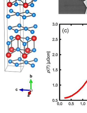
CeTe3 is a layered material in the family of rare earth () tritellurides, i.e., Te3. It is known as a heavy fermion system with a localized 4 orbital at the Ce3+ site. Its crystal structure consists of a NaCl-type CeTe layer which is responsible for its magnetic properties, separated by two Te sheets which are responsible for the highly two-dimensional (2D) electric transport iyeiri_prb_2003 , as shown in Fig. 1(a). Due to the highly 2D electrical transport, the material forms an incommensurate charge density wave (CDW) from well above room temperature, which has been studied extensively dimasi_prb_1995 ; brouet_prl_2004 ; kim_prl_2006 ; brouet_prb_2008 ; christos_jacs_2006 ; tomic_prb_2009 ; ralevic_prb_2016 .
This material is also known to show two magnetic phase transitions at low temperatures iyeiri_prb_2003 ; deguchi_jp_2009 ; zocco_prb_2009 ; okuma_sci_rep_2020 . The first magnetic transition at K is understood to be from a paramagnetic state to an antiferromagnetic (possibly short range ordering) state. In this phase, the magnetic moment at the Ce site is antiferromagnetically coupled and aligned to an easy axis perpendicular to the layer stacking direction. The second magnetic transition is known to be another antiferromagnetic (possibly long range ordering) transition iyeiri_prb_2003 ; deguchi_jp_2009 at K. Unlike the case of the first transition, a clear peak in the heat capacity has been observed below and the magnetic moment is still aligned to the in-plane direction (called non-parallel easy axis), but different from the easy axis in the first transition zocco_prb_2009 . Nevertheless, the details of these magnetic ordering states are poorly understood. Furthermore, there are no reports on thin film transport measurements.
In the present work, we have performed magnetotransport measurements with 30-40 nm thick CeTe3 devices. We have observed the coexisitance of quantum oscillation with unique magnetotransport phenomena. Specifically, a clear Shubnikov-de-Haas (SdH) oscillation was observed in the magnetic field range from 3 to 8 T even above , demonstrating the existence of a small Fermi surface pocket. Since such a SdH oscillation has never been reported in bulk CeTe3, the result reveals its strong 2D nature which is possibly enhanced by the thin film fabrication. Furthermore, the SdH oscillation has two frequencies below . This could originate from the modification of the Fermi surface due to the second magnetic transition at . We also observed a magnetic hysteresis in the SdH oscillation below . In particular, a sharp resistance peak appears at T only when the magnetic field is swept from a high enough magnetic field (more than 2 T) to zero field (see Fig. 3).
Single crystals of CeTe3 were synthesized in an evacuated quartz tube. The tube was heated up to 900∘C and slowly cooled to 550∘C over a period of 7 days. To fabricate thin film devices from the bulk CeTe3, we used the mechanical exfoliation technique using scotch tapes novoselov_science_2004 ; novoselov_nature_2005 ; zhang_nature_2005 ; novoselov_pnas_2005 . It is noted that all the following fabrication processes should be carried out inside a glove box with Ar purity of 99.9999%, since CeTe3 is extremely sensitive to ambient air. After the mechanical exfoliation process, many CeTe3 thin flakes on the scotch tape were transferred onto a thermally-oxidized silicon substrate. We then spin-coated polymethyl-methacrylate (PMMA) resist onto the substrate. The substrate was taken out from the glove box and electrode patterns were printed using electron beam lithography. After the lithography, the substrate was put back into the glove box again for the development of the resist. The Au electrodes were deposited using electron beam deposition in a vacuum chamber next to the glove box. Before the deposition of Au, Ar milling was performed to remove the residual resist and any possibly oxidized layers of CeTe3. It should be noted that contact resistance varies greatly with electrode material. Au electrodes were found to have a minimum contact resistance compared to Ti/Au or Cu. In order to avoid further damage in ambient condition after the fabrication, the device was capped with the PMMA shortly after the electrode deposition and the lift-off process. Figure 1(b) shows a scanning electron microscopy (SEM) image of one of the thin film devices.
Electrical transport measurements were performed by the conventional four-probe method using a lock-in amplifier. The device was cooled with a 3He/4He dilution refrigerator down to 0.2 K and the external magnetic field was applied using a superconducting magnet. The thicknesses of all measured CeTe3 thin films were confirmed by using a commercially available atomic force microscope after finishing all the electrical measurements.
The resistivity measured with the CeTe3 thin film device in Fig. 1(b) is plotted as a function of temperature in Fig. 1(c). Although the CeTe structure is half-metallic on its own, the high conductivity between the two Te sheets gives rise to a highly metallic temperature dependence in CeTe3 deguchi_jp_2009 . There are two resistivity changes in the low temperature region: the first resistivity drop at K, and the second resistivity kink structure at K. These behaviors are consistent with the anomalies observed in bulk CeTe3 resistivity measurements, which correspond to the two magnetic phase transitions at K and K iyeiri_prb_2003 ; deguchi_jp_2009 . The resistivity at room temperature of this device is 81.3 cm, resulting in the residual resistivity ratio (RRR) of 59.2 with respect to . This is 1.3 times higher than the previously reported value of 44.9 iyeiri_prb_2003 . At the lowest temperature ( K), RRR reaches a value of 140, indicating that the device is a high quality single crystal CeTe3 thin film.
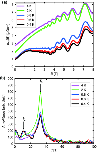
We next performed magnetoresistance measurements up to T for the temperature range from 0.4 to 4 K, as shown in Fig. 2(a). The external magnetic field was applied perpendicular to the plane, i.e., along the -axis of CeTe3 and swept from zero to 8 T. A large positive magnetoresistance was observed in the low field regime ( T) along with a clear SdH oscillation which develops from magnetic fields as low as T in the case of K. As far as we know, such a quantum oscillation (including the de Haas-van Alphen effect) has never been reported so far even for bulk CeTe3, although Lei et al. have recently reported a SdH oscillation in GdTe3 thin films lei_sci_adv_2020 . This fact is possibly related to much stronger 2D nature in thin films, compared to bulk crystals. Furthermore, the magnetoresistance behavior drastically changes below K, which is below the second magnetic transition temperature .
In order to extract the oscillatory part of the magnetoresistance, the derivative of with respect to was obtained numerically. Fast Fourier transform (FFT) was then performed in order to obtain the frequency of the quantum oscillation. The results are presented in Fig. 2(b). The main oscillation observed at all temperatures corresponds to a frequency of T, which is about two times smaller than that of GdTe3 lei_sci_adv_2020 . Below K, there is an additional oscillation with T, which can be seen as the secondary peak in the FFT spectrum in Fig. 2(b). The frequencies of these oscillations are proportional to the extremal cross sectional areas of the Fermi surface perpendicular to the applied magnetic field: , where is the Fermi surface area, is the elementary charge, is the frequency in the unit of T, and is the reduced Planck constant lifshitz_jetp_1956 . Using this equation, we obtained the Fermi surface areas of cm-2 for T, and cm-2 for T. The main oscillation is present even above the two magnetic transition temperatures, but well below its CDW transition temperature ( 500 K) brouet_prl_2004 ; kim_prl_2006 ; brouet_prb_2008 ; christos_jacs_2006 . The origin of this Fermi surface pocket can be attributed to the reconstruction of the Fermi surface due to the incommensurate CDW, which has been observed through photoemission spectroscopy experiments brouet_prl_2004 ; brouet_prb_2008 as well as through quantum oscillations of other Te3 materials lei_sci_adv_2020 ; ru_prb_2008 ; sinchenko_JLTP_2016 .
Although the angular dependence of the SdH oscillation has not been measured in the present study, it was already demonstrated in a similar tritelluride thin film device, i.e., GdTe3 lei_sci_adv_2020 where the SdH oscillation follows ( is the angle between the applied magnetic field and the layer stacking direction). This indicates a highly 2D geometry of the Fermi pockets. Since the crystal structure and the high conduction of the Te layers are the same for GdTe3 and CeTe3, we believe that the SdH oscillation observed in CeTe3 also originates from a highly 2D Fermi surface pocket. Especially, in the CeTe3 device is two times smaller than that in a thin film GdTe3 device, where the effective mass is known to be as small as ( is the bare electron mass) lei_sci_adv_2020 . This fact suggests that the conduction electrons between the Te sheets in the CeTe3 device have a similarly small effective mass. In addition, we detected the secondary oscillation with a frequency of , which does not exist in GdTe3 and develops only after the second magnetic transition temperature . According to Ref. deguchi_jp_2009, , the second magnetic transition at is related to a spin density wave transition with formation of heavy quasiparticles. Thus, such reconstruction of the Fermi surface along with this transition could be a possible cause of this new oscillation, but further investigation is required to confirm the hypothesis. We note that these SdH frequencies have also been observed in multiple different CeTe3 devices, confirming its reproducibility.
In a typical SdH oscillation, the FFT amplitude for a given frequency decreases with increasing temperature. However, FFT amplitudes of the main oscillation remained mostly constant, with the exception at K. A similar result has been reported in GdTe3, where the FFT amplitude plateaus below its antiferromagnetic transition temperature, while showing a typical temperature dependence well above the transition temperature lei_sci_adv_2020 . Our scenario is consistent with this report: in other words, the unconventional temperature dependence of the FFT amplitude depends strongly on the interaction between the magnetic order at the CeTe site and the conduction electrons.
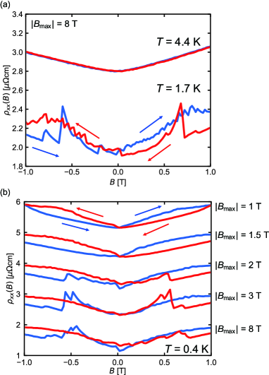
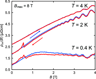
In addition to the SdH oscillations discussed above, we observed a magnetic hysteresis behavior, superimposed onto the SdH oscillations, below the first antiferromagnetic ordering temperature . This is highlighted in Fig. 3. At 4 K above , there is no hysteresis in the SdH oscillation. Below , however, a clear magnetic hysteresis is observed with a sharp peak structure at T. The magnetic hysteresis in the SdH oscillation vanishes above T, and the sharp peak appears only when is swept from a high enough field (in this case, T) to zero field, which we call the negative field sweeping. Note that quantum oscillations with magnetic hysteresis are reproducible for other CeTe3 thin film devices, even below , and also when the applied magnetic field is negative (see Fig 4). Furthermore, the peak amplitude depends on the absolute value of . At K, when is smaller than 1.5 T, the peak at T vanishes, while still preserving the hysteresis behavior, as shown in Fig. 4(b). Such a hysteresis has never been reported previously in bulk CeTe3 as well as in thin film GdTe3 devices lei_sci_adv_2020 . On the other hand, a hysteresis closely resembling our measurements have been observed for the magnetoresistance measurements in CeTe2 jung_prb_2000 , a variation of CeTe3. CeTe2 has the same crystal structure as CeTe3 but has a single Te layer instead of the double Te layers, and is known to order ferrimagnetically with an easy axis along the layer stacking direction park_pb_1998 . This is different from the magnetic order of bulk CeTe3, where the magnetic moments at the Ce sites in the two magnetic phases are believed to be aligned to the basal plane deguchi_jp_2009 ; zocco_prb_2009 . One possible scenario to explain the magnetoresistance hysteresis and peak structure observed in CeTe3 devices is that by the thin film fabrication, we have induced a canting of the magnetic moments along the layer stacking direction, resulting in a similar magnetoresistance effect to CeTe2. There is a supportive result where the perpendicular anisotropy of a van der Waals ferromagnet Fe5GeTe2 is enhanced by making it atomically thinner ohta_apex_2020 . In order to elucidate more details, it would be desirable to perform further experiments in future about the thickness dependence of the peak structure.
In conclusion, we have performed magnetotransport measurements of 30-40 nm thick CeTe3 thin film devices. A clear SdH oscillation was observed from K, indicating a highly two-dimentional character of the conduction electrons, possibly enhanced due to thin film fabrication. Below the second magnetic transition temperature K, on the other hand, SdH oscillations with two different frequencies were obtained. The FFT analysis revealed the existence of two small Fermi pockets whose sizes are cm-2 and cm-2. In addition, a magnetic hysteresis superimposed to the SdH oscillation was detected below the first antiferromagnetic temperature K. Especially, a sharp peak at T was clearly observed when the magnetic field was swept from the high enough field to zero field. Materials where quantum oscillations and magnetic hysteresis coexist are extremely scarce. Along with the ease of thin film fabrication through mechanical exfoliation, further researches on CeTe3 could pave the way for -orbital spintronics and could provide an ideal stage for understanding the interplay between electronic quantum conduction and localized heavy fermion spins.
We thank H. Sakai, K. Kuroki, M. Ochi, and K. Deguchi for fruitful discussions. The cell structure of CeTe3 was visualized using VESTA vesta . This work was supported by JSPS KAKENHI (Grant Numbers JP16H05964, JP17K18756, JP19K21850, JP20H02557, JP26103002, JP19H00656, JP19H05826), Mazda Foundation, Shimadzu Science Foundation, Yazaki Memorial Foundation for Science and Technology, SCAT Foundation, Murata Science Foundation, Toyota Riken Scholar, and Kato Foundation for Promotion of Science.
The data that support the findings of this study are available from the corresponding author upon reasonable request.
References
- (1) A. K. Geim and I. V. Grigorieva, Nature 499, 419 (2013).
- (2) K. S. Novoselov, A. Mishchenko, A. Carvalho, and A. H. Castro Neto, Science 353, aac9439 (2016).
- (3) K. S. Novoselov, A. K. Geim, S. V. Morozov, D. Jiang, Y. Zhang, S. V. Dubonos, I. V. Grigorieva, and A. A. Firsov, Science 306, 666 (2004).
- (4) K. S. Novoselov, A. K. Geim, S. V. Morozov, D. Jiang, M. I. Katsnelson, I. V. Grigorieva, S. V. Dubonos, and A. A. Firsov, Nature 438, 197 (2005).
- (5) Y. Zhang, Y.-W. Tan, H. L. Stormer, and P. Kim, Nature 438, 201 (2005).
- (6) K. S. Novoselov, D. Jiang, F. Schedin, T. J. Booth, V. V. Khotkevich, S. V. Morozov, and A. K. Geim, Proc. Natl. Acad. Sci. USA, 102, 10451 (2005).
- (7) B. Radisavljevic, A. Radenovic, J. Brivio, V. Giacometti, and A. Kis, Nat. Nanotech. 6, 147 (2011).
- (8) J. T. Ye, Y. J. Zhang, R. Akashi, M. S. Bahramy, R. Arita, and Y. Iwasa, Science 338, 1193 (2012).
- (9) C. R. Dean, A. F. Young, I. Meric, C. Lee, L. Wang, S. Sorgenfrei, K. Watanabe, T. Taniguchi, P. Kim, K. L. Shepard, and J. Hone, Nat. Nanotech. 5, 722 (2010).
- (10) L. A. Ponomarenko, A. K. Geim, A. A. Zhukov, R. Jalil, S. V. Morozov, K. S. Novoselov, I. V. Grigorieva, E. H. Hill, V. V. Cheianov, V. I. Fal’ko, K. Watanabe, T. Taniguchi, and R. V. Gorbachev, Nat. Phys. 7, 958 (2011).
- (11) Y. Cao, A. Mishchenko, G. L. Yu, E. Khestanova, A. P. Rooney, E. Prestat, A. V. Kretinin, P. Blake, M. B. Shalom, C. Woods, J. Chapman, G. Balakrishnan, I. V. Grigorieva, K. S. Novoselov, B. A. Piot, M. Potemski, K. Watanabe, T. Taniguchi, S. J. Haigh, A. K. Geim, and R. V. Gorbachev, Nano Lett. 15, 4914 (2015).
- (12) J.-F. Ge, Z.-L. Liu, C. Liu, C.-L. Gao, D. Qian, Q.-K. Xue, Y. Liu, and J.-F. Jia, Nat. Mater. 14, 285 (2015).
- (13) J. Shiogai, Y. Ito, T. Mitsuhashi, T. Nojima, and A. Tsukazaki, Nat. Phys. 12, 42 (2016).
- (14) Y. Yu, L. Ma, P. Cai, R. Zhong, C. Ye, J. Shen, G. D. Gu, X. H. Chen, and Y. Zhang, Nature 575, 156 (2019).
- (15) C. Gong, L. Li, Z. Li, H. Ji, A. Stern, Y. Xia, T. Cao, W. Bao, C. Wang, Y. Wang, Z. Q. Qiu, R. J. Cava, S. G. Louie, J. Xia, X. Zhang, Nature 546, 265 (2017).
- (16) B. Huang, G. Clark, E. Navarro-Moratalla, D. R. Klein, R. Cheng, K. L. Seyler, D. Zhong, E. Schmidgall, M. A. McGuire, D. H. Cobden , W. Yao, D. Xiao, P. Jarillo-Herrero, and X. Xu, Nature 546, 270 (2017).
- (17) Z. Wang, T. Zhang, M. Ding, B. Dong, Y. Li, M. Chen, X. Li, J. Huang, H. Wang, X. Zhao, Y. Li, D. Li, C. Jia, L. Sun, H. Guo, Y. Ye, D. Sun, Y. Chen, T. Yang, J. Zhang, S. Ono, Z. Han, and Z. Zhang, Nat. Nanotech. 13, 554 (2018).
- (18) Z. Fei, B. Huang, P. Malinowski, W. Wang, T. Song, J. Sanchez, W. Yao, D. Xiao, X. Zhu, A. F. May, W. Wu, D. H. Cobden, J.-H. Chu, and X. Xu, Nat. Mater. 17, 778 (2018).
- (19) Y. Deng, Y. Yu, Y. Song, J. Zhang, N. Z. Wang, Z. Sun, Y. Yi, Y. Z. Wu, S. Wu, J. Zhu, J. Wang, X. H. Chen, and Y. Zhang, Nature 563, 94 (2018).
- (20) Y. Cao, V. Fatemi, S. Fang, K. Watanabe, T. Taniguchi, E. Kaxiras, P. Jarillo-Herrero, Nature 556, 43 (2018).
- (21) Y. Wu, S. Zhang, G. Yin, J. Zhang, W. Wang, Y. L. Zhu, J. Hu, K. Wong, C. Fang, C. Wan, X. Han, Q. Shao, T. Taniguchi, K. Watanabe, J. Zang, Z. Mao, X. Zhang, K. L. Wang, arXiv:1907.11349.
- (22) T. Song, X. Cai, M. W. Tu, X. Zhang, B. Huang, N. P. Wilson, K. L. Seyler, L. Zhu, T. Taniguchi, K. Watanabe, M. A. McGuire, D. H. Cobden, D. Xiao, W. Yao, and X. Xu, Science 360, 1214 (2018).
- (23) X. Wang, J. Tang, X. Xia, C. He, J. Zhang, Y. Liu, C. Wan, C. Fang, C. Guo, W. Yang, Y. Guang, X. Zhang, H. Xu, J. Wei, M. Liao, X. Lu, J. Feng, X. Li, Y. Peng, H. Wei, R. Yang, D. Shi, X. Zhang, Z. Han, Z. Zhang, G. Zhang, G. Yu, and X. Han, Sci. Adv. 5, eaaw8904 (2018).
- (24) Y. Iyeiri, T. Okumura, C. Michioka, and K. Suzuki, Phys. Rev. B 67, 144417 (2003).
- (25) E. DiMasi, M. C. Aronson, J. F. Mansfield, B. Foran, and S. Lee, Phys. Rev. B 52, 14516 (1995).
- (26) V. Brouet, W. L. Yang, X. J. Zhou, Z. Hussain, N. Ru, K. Y. Shin, I. R. Fisher, and Z. X. Shen, Phys. Rev. Lett. 93, 126405 (2004).
- (27) H. J. Kim, C. D. Malliakas, A. T. Tomić, S. H. Tessmer, M. G. Kanatzidis, and S. J. L. Billinge, Phys. Rev. Lett. 96, 226401 (2006).
- (28) V. Brouet, W. L. Yang, X. J. Zhou, Z. Hussain, R. G. Moore, R. He, D. H. Lu, Z. X. Shen, J. Laverock, S. B. Dugdale, N. Ru, and I. R. Fisher, Phys. Rev. B 77, 235104 (2008).
- (29) C. D. Malliakas and M. G. Kanatzidis, J. Am. Chem. Soc. 128, 12612 (2006).
- (30) A. Tomic, Zs. Rak, J. P. Veazey, C. D. Malliakas, S. D. Mahanti, M. G. Kanatzidis, and S. H. Tessmer, Phys. Rev. B 79, 085422 (2009).
- (31) U. Ralević, N. Lazarević, A. Baum, H.-M. Eiter, R. Hackl, P. Giraldo-Gallo, I. R. Fisher, C. Petrovic, R. Gajić, and Z. V. Popović, Phys. Rev. B 94, 165132 (2016).
- (32) K. Deguchi, T. Okada, G. F. Chen, S. Ban, N. Aso, and N. K. Sato, J. Phys.: Conf. Ser. 150, 042023 (2009).
- (33) D. A. Zocco, J. J. Hamlin, T. A. Sayles, and M. B. Maple, Phys. Rev. B 79, 134428 (2009).
- (34) R. Okuma, D. Ueta, S. Kuniyoshi, Y. Fujisawa, B. Smith, C. H. Hsu, Y. Inagaki, W. Si, T. Kawae, H. Lin, F. C. Chuang, T. Masuda, R. Kobayashi, and Y. Okada, Sci. Rep., in press.
- (35) S. Lei, J. Lin, Y. Jia, M. Gray, A. Topp, G. Farahi, S. Klemenz, T. Gao, F. Rodolakis, J. L. McChesney, C. R. Ast, A. Yazdani, K. S. Burch, S. Wu, N. P. Ong, and L. M. Schoop, Sci. Adv. 6, eaay6407 (2020).
- (36) I. M. Lifshitz and A. M. Kosevich, Sov. Phys. JETP 2, 636 (1956).
- (37) N. Ru, R. A. Borzi, A. Rost, A. P. Mackenzie, J. Laverock, S. B. Dugdale, and I. R. Fisher, Phys. Rev. B 78, 045123 (2008).
- (38) A. A. Sinchenko, P. D. Grigoriev, P. Monceau, P. Lejay, and V. N. Zverev, J. Low Temp. Phys., 185, 657 (2016).
- (39) M. H. Jung, K. Umeo, T. Fujita, and T. Takabatake, Phys. Rev. B 62, 11609 (2000).
- (40) J. G. Park, I. P. Swainson, W. J. L. Buyers, M. H. Jung, and Y. S. Kwon, Physica B 241, 684 (1998).
- (41) T. Ohta, K. Sakai, H. Taniguchi, B. Driesen, Y. Okada, K. Kobayashi, and Y. Niimi, Appl. Phys. Express 13, 043005 (2020).
- (42) K. Momma and F. Izumi, J. Appl. Cryst. 44, 1272-1276 (2011).