A Cleanroom in a Glovebox
The exploration of new materials, novel quantum phases, and devices requires ways to prepare cleaner samples with smaller feature sizes. Initially, this meant the use of a cleanroom that limits the amount and size of dust particles. However, many materials are highly sensitive to oxygen and water in the air. Furthermore, the ever-increasing demand for a quantum workforce, trained and able to use the equipment for creating and characterizing materials, calls for a dramatic reduction in the cost to create and operate such facilities. To this end, we present our cleanroom-in-a-glovebox, a system which allows for the fabrication and characterization of devices in an inert argon atmosphere. We demonstrate the ability to perform a wide range of characterization as well as fabrication steps, without the need for a dedicated room, all in an argon environment. Connection to a vacuum suitcase is also demonstrated to enable receiving from and transfer to various ultra-high vacuum (UHV) equipment including molecular-beam epitaxy (MBE) and scanning tunneling microscopy (STM).
I Introduction
Fabrication of devices at the nano-scale is central to future efforts in exploring novel quantum phases of matter and building next-generation devices. Previously this was achieved by creating dedicated facilities where the entire space is filtered and dust minimized via special air handling and attire for all who enter. While these cleanrooms minimize the amount of dust and other particles that can damage mesoscale devices, they do not protect the samples from either oxygen or water. At the same time they require extremely expensive and energy-intensive investments. In contrast, gloveboxes provide an inert atmosphere for working with oxygen and water sensitive materials, with greatly reduced initial and operational cost.Chae et al. (2016) However, performing nanolithography in a glovebox risks contaminating the rest of the inert environment due to the various solvents involved. With these issues in mind, we have designed and constructed the cleanroom-in-a-glovebox to bridge the gap between these two approaches in order to prepare, fabricate, and characterize various scientific samples entirely within an inert argon atmosphere. The cleanroom-in-a-glovebox contains two separate work chambers, one is devoted entirely to lithography and the other to preparation and characterization (Fig. 1a). The system can be operated with minimal training, no need for special attire (i.e. gowning), and far fewer demands on the building. As such, the described cleanroom in a glovebox produces high-quality devices yet requires far lower initial investment and operational cost than a traditional cleanroom.Liddle et al. (2020) This makes the system described crucial in future efforts at training the quantum workforce and development of novel devices with a wider range of materials.
An overview of the system is shown in Fig. 1 and a more in-depth schematic of the glovebox is shown in Fig. 2. The lithography chamber, (discussed in the “Fabrication” section), contains a Heidelberg PG101 Direct-Write system, an Angstrom NexDep Thermal Deposition and Plasma Etching system, and a Spin-Coating Systems G3 Spin Coater. The characterization chamber contains a WITec alpha300R confocal Raman system (Fig. 1b & Fig. 3b), a Nanomagnetics ezAFM (Fig. 3a), a home-built 2D material dry-transfer system, electronic BNC and banana cable feedthroughs. These two chambers are connected via a small antechamber which allows us to transfer samples into and out of the gloveboxes while also enabling simple transfer between boxes without contamination. Lastly, attached to the back of the glovebox is an intermediate chamber for attaching a vacuum suitcase (Fig. 1d). This allows receiving from and transferring to a wide array of ultra-high vacuum (UHV) systems, providing compatibility with electron-beam systems, scanning tunneling microscopy (STM), molecular beam epitaxy (MBE), angle resolved photoemission spectroscopy (ARPES) and other cutting edge tools. Furthermore, the modular nature of the glovebox allows for future equipment to be attached to the glovebox with relative ease. As such our processes and design enable a range of scientific tools on nanoscale, air-sensitive materials, while simultaneously reducing the time, training and cost involved.
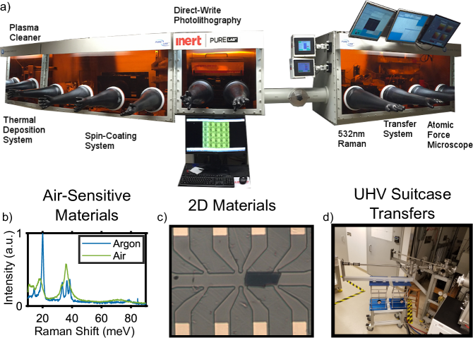
During normal operation, the characterization glovebox maintains O2 and H2O levels below the resolution of the sensors (0.1 ppm) while the fabrication box maintains 1 ppm. This is achieved by continuously running the argon through a copper column chamber which the oxygen and water adhere to, thus removing them from the argon. If the oxygen and water levels are unable to be maintained below 5 ppm the glovebox is purged with argon until the values are back to the normal operating levels. The argon is additionally run through two 300 nm HEPA filters during this recirculation process. When transferring objects into the glovebox, users are required to wipe down the objects with isopropanol wipes to limit the amount of dust that is transferred with the objects. Users are also required to wear nitrile gloves on top of the butyl gloves of the box in order to avoid cross contamination of adhesives. After exfoliation, the nitrile gloves are removed and all associated exfoliation waste is wrapped in the gloves and immediately taken out of the glovebox. As a result of these procedures and the HEPA filters, after four years of continuous operation there were no particles 0.5 m measured and an average of 6,800 particles that were 0.3 m per cubic meter. This is the equivalent of a class 100 cleanroom according to ISO cleanroom standards.ISO 114644-1:2015 (2015). We anticipate even better particle levels could be achieved via use of higher quality filters. Furthermore, we did not have to change the HEPA filters over the first four years of operation whereas a typical cleanroom routinely changes the pre-filters every 6 to 12 months.
II Materials Characterization
Atomic force microscopy (AFM) is an invaluable tool for characterizing materials. In the case of mesoscale physics, AFM is used to discern the thickness of exfoliated 2D materials. In other cases it characterizes the roughness of a substrate (such as in 3a) or sample. In order to resolve such small features, great care was taken to isolate the AFM system from environmental vibrations. This is more difficult than usual in a glovebox as there are quite a few vibrations that arise from the gas-circulation system. To combat the environmental vibrations the ezAFM and transfer stage were placed on a heavy granite slab. An additional Minus-K Vibration isolation stage was employed for the ezAFM and care was taken to ensure the cables were well secured to each other but did not touch the glovebox directly. The results of this are seen in Fig. 3a where we took an AFM scan of mica, an atomically flat substrate. The noise levels of the scan are less than 5 Å in magnitude (the resolution of the ezAFM). To ensure rougher features can be resolved, this was compared with the AFM from HfO2 film on a Si substrate grown by atomic-layer deposition. We note that ezAFM works with voice coils and thus is substantially less expensive and easier to use than a typical AFM system. Nonetheless, we anticipate a further reduction in noise with more traditional piezo-based scanning probes.
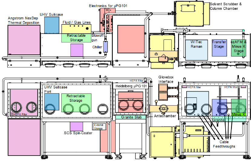
Raman spectroscopy can reveal the quality, doping level, thickness, symmetry, and cleanliness of samples.Ferrari and Basko (2013); Shahil et al. (2010); Zhou et al. (2019); Lei et al. (2020); Sandilands et al. (2010); Tian et al. (2016a) For example, the ratio of the 2D peak to the G peak in graphene is commonly employed to discern how disordered the sample is.Wu et al. (2018a) With our Raman system’s mapping capabilities, we determined the spatial distribution of the disorder after the fabrication of CVD graphene such as in Fig. 3b. The WITec system also allows us to measure photoluminescence (PL) with a simple switch of energy ranges. PL is a useful measurement technique when working with materials such as MoS2, as it quickly identifies single-layer flakes, and provides insight into the interaction with the substrate.YHlee2017review; Yin et al. (2011); Butler et al. (2013) We observed another advantage of the glovebox here. Namely, mica is known to have charged potassium ions on the surface after cleaving, but is quickly neutralized in air.Lui et al. (2009) When exfoliating MoS2 directly to the mica we found the PL consistent with the mica taking the MoS2 from n-type to intrinsic.Mak et al. (2013); Ross et al. (2013) (see Fig. 3c)
It is crucial to overcome the “glovebox-specific” problems to obtain the high-quality Raman and PL data. These are two-fold, first additional light contamination adding unwanted background signals and change in focus or position of the sample due to vibrations, air currents, and temperature fluctuations. To minimize these effects a simple casing was placed around the entire Raman system, using black plastic sheets and 80-20 aluminum bars. Combined with careful isolation of the fibers and wires via foam sealing to the glovebox, the case enabled high-resolution Raman and PL area-scans like the one shown in Fig. 3b and c.
III Sample Fabrication
The ability to create mesoscopic heterostructures has been crucial in the study of 2D materials, by enabling new physical effects and allowing encapsulation for removal to air.Dean:2012ht; Sharpe et al. (2019); Wu et al. (2018b); Stepanov et al. (2018); Tang et al. (2017); Zareapour et al. (2012); Island et al. (2019); Chae et al. (2016) However, this relies on minimizing additional contaminants from solvents. Thus we constructed a standard dry-transfer system in the characterization chamber.Castellanos-Gomez et al. (2014) To ensure excellent alignment and minimal drift during transfer, the stage was placed on a thick granite slab, with the required wires and tubing isolated from touching the glovebox chamber directly. The transfer stage has six, fully-motorized stages, three of which are piezo-based Picomotor stages with a 30 nm step size providing precise positioning of the samples relative to one another, such as the heterostructure shown in Fig. 1c. Furthermore, this system has produced a number of complex devices including the realization of Coulomb blockade into atomic defects in a 2D heterostructureBrotons-Gisbert et al. (2019), observation of hinge modes in a higher order topological superconductor,Gray et al. (2019) and CVD graphene sensors of bacteria with single cell resolutionKumar et al. (2020).
One of the key features of our cleanroom-in-a-glovebox is our photolithography capabilities. In our fabrication chamber, we have an SCS G3 Spin Coater, Angstrom Engineering NexDep physical vapor deposition system, a UHV suitcase transfer system, and a Heidelberg PG101 Direct-Write system. The glovebox column has a solvent scrubber installed, which allows for small amounts of solvent to be removed from the system. This keeps the rest of the environment clean while using the photolithographic, lift-off, and cleaning solvents. We employ the use of Qorpak bottles to limit the exposure of solvents and other liquids to the glovebox atmosphere. These bottles have a PTFE liner in the caps that are resistant to most chemicals while also providing a low moisture transmission rate when sealed. The bottles remain sealed except for the brief times needed. Furthermore, we employ the use of some administrative procedures such as using activated charcoal as a passive solvent absorbent when exposing the environment to liquids and purging the box with argon after fabrication. The result of such efforts are shown in Raman, PL, and AFM scans of materials where long term exposure to the fabrication chamber revealed no evidence for additional contamination. This is further attested to by our ability to observe quantum oscillations at relatively low fields in graphene devices fabricated inside (Fig. 4c). We note that there are a variety of options for fabrication which completely eliminate water from the process, including shadow (or stencil) mask techniques and transferring flakes onto pre-written contacts.Zhao et al. (2019); Zalic et al. (2019)
The lack of contamination along with the alignment abilities of the mask-less system was crucial in creating high-quality devices and periodic structures (see Fig. 4d and 4e). The PG101 has a resolution of m with a 20 nm registry, optical auto-focus and can write up to a 5-inch wafer in one run. We note optical auto-focusing is required as the changing dynamics of the glovebox air prevented the use of standard pressure alignment. The PG101 stage runs on an air-bearing that is normally supplied with compressed air from the building, but this is not possible while in a glovebox as the unfiltered air would vent directly into the clean environment. Instead, we inserted a T-junction into the argon path from the cylinder where one side of the junction goes into the cylinder to supply the glovebox and the other supplies the stage with argon for the air-bearing. Not only does this solve the air-bearing problem but it also speeds up the removal of excess solvents and water from the clean atmosphere. To shut off the air-bearing when the system is not in use, we installed a cutoff valve after the T-junction that is closed when the stages are not in use.
In a typical nanofabrication process, one must develop and dry the samples in air before moving them into a deposition tool. With an in-situ thermal deposition system glovebox users are able to develop and dry the sample in the inert argon environment before transferring them into the deposition tool. Furthermore, the deposition tool contains an in-situ plasma-cleaning system so samples can be de-scummed in high vacuum immediately before the deposition of metals. This step can be critical in establishing good electrical contact to certain materials.Zalic et al. (2019) After the deposition, small amounts of aluminum can be evaporated onto the samples followed by exposure to a 0.1% oxygen environment, creating an air-protection layer of alumina.Damasco et al. (2019) This layer of alumina can also be used to protect samples against photoresists during nanofabrication processes as it is easily removed by TMAH-based developers. For example, when fabricating CVD graphene devices we first deposit a layer of alumina before spin-coating photoresists while the rest of the fabrication process remains exactly the same, including energy dosage and developing times. The areas of photoresist that are developed out also allow for the developer to come in contact with the alumina, removing it as well. Thus we are still able to make good electrical contact to the graphene while preventing contact with the photoresist and other potential dopants.
The deposition tool also opens to the outside allowing users to clean samples with argon plasma or thermal annealing before loading them into the glovebox. An example is our fabrication of CVD graphene devices for use in bio-sensing applications. The CVD graphene is grown on copper foil and thus must be transferred onto SiO2/Si wafers via wet transfer.Ping et al. (2016) In order to clean the graphene, we bake the samples in the deposition tool at 350 oC in 10-7 mBar pressure for nine hours before alumina deposition (described above) then subsequently transfer samples into the glovebox for patterning. The result of this is samples that are clean enough to not only see quantum oscillations at 8 K and 7 T shown in Fig. 4c, but are also able to be used as single-bacterium bio-detectors.Kumar et al. (2020)
IV Ultra High Vacuum Suitcase
After fabrication, samples typically must be taken out of the glovebox to be measured in more specialized pieces of equipment such as surface-sensitive (STM, APRES) or low-temperature transport and optical probes. Furthermore, many new materials and heterostructures are first created by MBE, requiring in-situ probes to determine their device characteristics.Gerber et al. (2017); Wang, Ma, and Xue (2016); Hellman et al. (2017) This presents a chance for the samples to see air and degrade. Typically this is avoided by coating the samples with a “capping-layer” (e.g. alumina) or covering mesoscale samples with hBN. However, samples may interact with these materials in unexpected ways such as accidental electrical shorting if the alumina contains many pinholes or if the hBN induces strain into the samples. The addition of hBN to an exfoliated flake could cause additional complexities including changing the dielectric environment or inducing Moiré patterns that, while exciting, make reproducibility of devices quite difficult as both layers must be aligned in the same orientation every time.Sharpe et al. (2019); Woods et al. (2014); doi:10.1021/nl5006542; Tran et al. (2019); Jin et al. (2019); Alexeev et al. (2019); Yankowitz et al. (2019); Cao et al. (2018) Another exciting example of eliminating hBN from air-sensitive devices is the -Fe1.1Se crystal, where recent experiments have shown enhancements of Tc in monolayer films as compared to bulk samples but clean monolayer-devices have yet to be realized.Gerber et al. (2017); Wang, Ma, and Xue (2016) This is in part due to the air-sensitivity of the system at low layer numbers but is also due to the crystal’s sensitivity to strain.Yang et al. (2019) Recent experiments have shown that the Tc of -Fe1.1Se thin films change as much as 10 K with 1% strain which demonstrates the problem in making hBN encapsulated devices.Kawai, Nabeshima, and Maeda (2018)
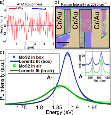
To expand the range of probes and fabrication capabilities of the cleanroom-in-a-glovebox, we designed and built a UHV chamber to couple to various vacuum suitcases (see Fig. 1d). The intermediate chamber has a block for attaching different kinds of sample holders allowing us to transfer materials into the glovebox from MBE and out to STM, low-temperature Raman, or electrical transport systems (e.g. see Fig. 4a). One measurement system of particular interest is the custom-designed Montana Instruments low-temperature optical cryostat. This system has been described in detail in other worksTian et al. (2016b) but has been adapted to be compatible with a UHV suitcase. All of the suitcases follow typical transfer procedures with the addition of a connection to an inlet for argon gas.Firpo et al. (2005) Specifically, after the sample is brought into the intermediate space, the suitcase is valved off and Ar added to bring the chamber to match the glovebox pressure. Once matched the intermediate chamber is opened to the glovebox, where the sample holder is brought in using a second manipulator arm. When transferring devices out of the glovebox a baking step is added to the normal process after vacuuming where the entire chamber is heated to 120oC. This step helps remove any excess impurities introduced when exposing the intermediate chamber to the glovebox.
The merits of such work are shown in Fig. 4b, where we probe the Raman response of GdTe3, established to be highly air sensitive.Lei et al. (2020) Two bulk crystals were prepared in the glovebox, then one was transferred into the low-temperature Raman system in air and freshly cleaved just before cool down. The second sample was transferred via the UHV suitcase. The crystal that was transferred in air clearly shows a large tellurium oxide peak around 17 meV that obscures phonon modes.Tian et al. (2016c); Lei et al. (2020) However, the material transferred via vacuum suitcase revealed sharp phonon modes, with the exception of the CDW amplitude mode at low energies. In addition, we found the Raman response to be much more uniform across the sample surface.
V Conclusions
Here we demonstrated the construction and operation of a cleanroom-in-a-glovebox. The system combines the inert environment of a glovebox with the fabrication and characterization facilities of a cleanroom. While modifications had to be made to existing equipment and procedures, the result is a fast and efficient fabrication facility that allows devices made from many air-sensitive systems. As a result, we believe our work will motivate future efforts in the development of equipment and techniques in inert atmosphere for next-generation devices. In addition, the far reduced cost, ease of use, and environmental requirements open the door to using this setup in a wider array of educational as well as research settings.
Acknowledgments
The authors are especially grateful to T. Ezell from Witec Instruments, Matt Woods from. Angstrom Instruments Inc., Jake DeGrave and Bobby Riviere for assistance in designing and implementing various components. The authors are grateful to Paige Kelley-Lampen, David Mandrus, and Stephen E. Nagler for providing the RuCl3 sample. M.J.G., G.B.O., V.P. and K.S.B acknowledge the primary support of the US Department of Energy (DOE), Office of Science, Office of Basic Energy Sciences under award no. DE-SC0018675. Y.W. acknowledges support from the National Science Foundation, Award No. DMR-1709987, while R.O’C, M.C.D., M.L.R. were supported by grant BIO-1560200. X.L. acknowledges the support of Boston University. I.Z., B.R. and H.Z. gratefully acknowledges the support from the National Science Foundation Grant No. NSF-DMR-1654041. Work at BNL is supported by the Office of Science, U.S. Department of Energy under Contract No. de-sc0012704. This research is funded in part by the Gordon and Betty Moore Foundation through Grant GBMF9064 to L.M.S.
Data Availability Statement
The data that support the findings of this study are available from the corresponding author upon reasonable request.
References
- Chae et al. (2016) S. H. Chae, Y. Jin, T. S. Kim, D. S. Chung, H. Na, H. Nam, H. Kim, D. J. Perello, H. Y. Jeong, T. H. Ly, and Y. H. Lee, ACS Nano 10, 1309 (2016).
- Liddle et al. (2020) J. A. Liddle, J. Bowser, B. R. Ilic, and V. Luciani, J Res Natl Inst Stan 125 (2020).
- ISO 114644-1:2015 (2015) ISO 114644-1:2015, “Cleanrooms and associated controlled environments — Part 1: Classification of air cleanliness by particle concentration,” Standard (International Organization for Standardization, Geneva, CH, 2015).
- Ferrari and Basko (2013) A. C. Ferrari and D. M. Basko, Nature Nanotechnology 8, 235 (2013).
- Shahil et al. (2010) K. M. F. Shahil, M. Z. Hossain, D. Teweldebrhan, and A. A. Balandin, Applied Physics Letters 96, 3103 (2010).
- Zhou et al. (2019) B. Zhou, Y. Wang, G. B. Osterhoudt, P. Lampen-Kelley, D. Mandrus, R. He, K. S. Burch, and E. A. Henriksen, Journal of Physics and Chemistry of Solids 128, 291 (2019).
- Lei et al. (2020) S. Lei, J. Lin, Y. Jia, M. Gray, A. Topp, G. Farahi, S. Klemenz, T. Gao, F. Rodolakis, J. L. McChesney, C. R. Ast, A. Yazdani, K. S. Burch, S. Wu, N. P. Ong, and L. M. Schoop, Science Advances 6 (2020).
- Sandilands et al. (2010) L. J. Sandilands, J. X. Shen, G. M. Chugunov, S. Y. F. Zhao, S. Ono, Y. Ando, and K. S. Burch, Phys. Rev. B 82, 064503 (2010).
- Tian et al. (2016a) Y. Tian, G. B. Osterhoudt, S. Jia, R. J. Cava, and K. S. Burch, Appl. Phys. Lett. 108, 041911 (2016a).
- Wu et al. (2018a) J.-B. Wu, M.-L. Lin, X. Cong, H.-N. Liu, and P.-H. Tan, Chemical Society Reviews 47, 1822 (2018a).
- Yin et al. (2011) Z. Yin, H. Li, H. Li, L. Jiang, Y. Shi, Y. Sun, G. Lu, Q. Zhang, X. Chen, and H. Zhang, ACS nano 6, 74 (2011).
- Butler et al. (2013) S. Z. Butler, S. M. Hollen, L. Cao, Y. Cui, J. A. Gupta, H. R. Gutiérrez, T. F. Heinz, S. S. Hong, J. Huang, A. F. Ismach, E. Johnston-Halperin, M. Kuno, V. V. Plashnitsa, R. D. Robinson, R. S. Ruoff, S. Salahuddin, J. Shan, L. Shi, M. G. Spencer, M. Terrones, W. Windl, and J. E. Goldberger, ACS Nano 7, 2898 (2013).
- Lui et al. (2009) C. H. Lui, L. Liu, K. F. Mak, G. W. Flynn, and T. F. Heinz, Nature 462, 339 (2009).
- Mak et al. (2013) K. F. Mak, K. He, C. Lee, G. H. Lee, J. Hone, T. F. Heinz, and J. Shan, Nature materials 12, 207 (2013).
- Ross et al. (2013) J. S. Ross, S. Wu, H. Yu, N. J. Ghimire, A. M. Jones, G. Aivazian, J. Yan, D. G. Mandrus, D. Xiao, W. Yao, and X. Xu, Nature Communications 4, 1474 (2013).
- Sharpe et al. (2019) A. L. Sharpe, E. J. Fox, A. W. Barnard, J. Finney, K. Watanabe, T. Taniguchi, M. A. Kastner, and D. Goldhaber-Gordon, Science 365, 605 (2019).
- Wu et al. (2018b) S. Wu, V. Fatemi, Q. D. Gibson, K. Watanabe, T. Taniguchi, R. J. Cava, and P. Jarillo-Herrero, Science 359, 76 (2018b).
- Stepanov et al. (2018) P. Stepanov, S. Che, D. Shcherbakov, J. Yang, R. Chen, K. Thilahar, G. Voigt, M. W. Bockrath, D. Smirnov, K. Watanabe, T. Taniguchi, R. K. Lake, Y. Barlas, A. H. MacDonald, and C. N. Lau, Nature Physics 14, 907 (2018).
- Tang et al. (2017) S. Tang, C. Zhang, D. Wong, Z. Pedramrazi, H.-Z. Tsai, C. Jia, B. Moritz, M. Claassen, H. Ryu, S. Kahn, J. Jiang, H. Yan, M. Hashimoto, D. Lu, R. G. Moore, C.-C. Hwang, C. Hwang, Z. Hussain, Y. Chen, M. M. Ugeda, Z. Liu, X. Xie, T. P. Devereaux, M. F. Crommie, S.-K. Mo, and Z.-X. Shen, Nature Physics 13, 683 (2017).
- Zareapour et al. (2012) P. Zareapour, A. Hayat, S. Y. F. Zhao, M. Kreshchuk, A. Jain, D. C. Kwok, N. Lee, S.-W. Cheong, Z. Xu, A. Yang, G. D. Gu, S. Jia, R. J. Cava, and K. S. Burch, Nature communications 3, 1056 (2012).
- Island et al. (2019) J. O. Island, X. Cui, C. Lewandowski, J. Y. Khoo, E. M. Spanton, H. Zhou, D. Rhodes, J. C. Hone, T. Taniguchi, K. Watanabe, L. S. Levitov, M. P. Zaletel, and A. F. Young, Nature 571, 85 (2019).
- Castellanos-Gomez et al. (2014) A. Castellanos-Gomez, M. Buscema, R. Molenaar, V. Singh, L. Janssen, H. S. J. van der Zant, and G. A. Steele, 2D Materials 1, 011002 (2014).
- Brotons-Gisbert et al. (2019) M. Brotons-Gisbert, A. Branny, S. Kumar, R. Picard, R. Proux, M. Gray, K. S. Burch, K. Watanabe, T. Taniguchi, and B. D. Gerardot, Nature Nanotechnology 14, 442 (2019).
- Gray et al. (2019) M. J. Gray, J. Freudenstein, S. Y. F. Zhao, R. O’Connor, S. Jenkins, N. Kumar, M. Hoek, A. Kopec, S. Huh, T. Taniguchi, K. Watanabe, R. Zhong, C. Kim, G. D. Gu, and K. S. Burch, Nano Letters 19, 4890 (2019).
- Kumar et al. (2020) N. Kumar, W. Wang, J. C. Ortiz-Marquez, M. Catalano, M. Gray, N. Biglari, K. Hikari, X. Ling, J. Gao, T. van Opijnen, and K. S. Burch, Biosensors and Bioelectronics , 156, 112123 (2020).
- Zhao et al. (2019) S. Y. F. Zhao, N. Poccia, M. G. Panetta, C. Yu, J. W. Johnson, H. Yoo, R. Zhong, G. D. Gu, K. Watanabe, T. Taniguchi, S. V. Postolova, V. M. Vinokur, and P. Kim, Phys. Rev. Lett. 122, 247001 (2019).
- Zalic et al. (2019) A. Zalic, S. Simon, S. Remennik, A. Vakahi, G. D. Gu, and H. Steinberg, Phys. Rev. B 100, 064517 (2019).
- Damasco et al. (2019) J. Damasco, S. T. Gill, S. Gazibegovic, G. Badawy, E. P. A. M. Bakkers, and N. Mason, Applied Physics Letters 115, 043503 (2019).
- Ping et al. (2016) J. Ping, R. Vishnubhotla, A. Vrudhula, and A. T. C. Johnson, ACS Nano 10, 8700 (2016).
- Gerber et al. (2017) S. Gerber, S.-L. Yang, D. Zhu, H. Soifer, J. A. Sobota, S. Rebec, J. J. Lee, T. Jia, B. Moritz, C. Jia, A. Gauthier, Y. Li, D. Leuenberger, Y. Zhang, L. Chaix, W. Li, H. Jang, J.-S. Lee, M. Yi, G. L. Dakovski, S. Song, J. M. Glownia, S. Nelson, K. W. Kim, Y.-D. Chuang, Z. Hussain, R. G. Moore, T. P. Devereaux, W.-S. Lee, P. S. Kirchmann, and Z.-X. Shen, Science 357, 71 (2017).
- Wang, Ma, and Xue (2016) L. Wang, X. Ma, and Q.-K. Xue, Superconductor Science and Technology 29, 123001 (2016).
- Hellman et al. (2017) F. Hellman, A. Hoffmann, Y. Tserkovnyak, G. S. D. Beach, E. E. Fullerton, C. Leighton, A. H. MacDonald, D. C. Ralph, D. A. Arena, H. A. Dürr, P. Fischer, J. Grollier, J. P. Heremans, T. Jungwirth, A. V. Kimel, B. Koopmans, I. N. Krivorotov, S. J. May, A. K. Petford-Long, J. M. Rondinelli, N. Samarth, I. K. Schuller, A. N. Slavin, M. D. Stiles, O. Tchernyshyov, A. Thiaville, and B. L. Zink, Rev. Mod. Phys. 89, 025006 (2017).
- Woods et al. (2014) C. Woods, L. Britnell, A. Eckmann, G. Yu, R. Gorbachev, A. Kretinin, J. Park, L. Ponomarenko, M. Katsnelson, Y. Gornostyrev, K. Watanabe, T. Taniguchi, C. Casiraghi, H. Guo, A. Geim, and K. Novoselov, Nature Physics 10, 451 (2014).
- Tran et al. (2019) K. Tran, G. Moody, F. Wu, X. Lu, J. Choi, K. Kim, A. Rai, D. A. Sanchez, J. Quan, A. Singh, J. Embley, A. Zepeda, M. Campbell, T. Autry, T. Taniguchi, K. Watanabe, N. Lu, S. K. Banerjee, K. L. Silverman, S. Kim, E. Tutuc, L. Yang, A. H. MacDonald, and X. Li, Nature 567, 71 (2019).
- Jin et al. (2019) C. Jin, E. C. Regan, A. Yan, M. Iqbal Bakti Utama, D. Wang, S. Zhao, Y. Qin, S. Yang, Z. Zheng, S. Shi, K. Watanabe, T. Taniguchi, S. Tongay, A. Zettl, and F. Wang, Nature 567, 76 (2019).
- Alexeev et al. (2019) E. M. Alexeev, D. A. Ruiz-Tijerina, M. Danovich, M. J. Hamer, D. J. Terry, P. K. Nayak, S. Ahn, S. Pak, J. Lee, J. I. Sohn, M. R. Molas, M. Koperski, K. Watanabe, T. Taniguchi, K. S. Novoselov, R. V. Gorbachev, H. S. Shin, V. I. Fal’ko, and A. I. Tartakovskii, Nature 567, 81 (2019).
- Yankowitz et al. (2019) M. Yankowitz, S. Chen, H. Polshyn, Y. Zhang, K. Watanabe, T. Taniguchi, D. Graf, A. F. Young, and C. R. Dean, Science 363, 1059 (2019). .
- Cao et al. (2018) Y. Cao, V. Fatemi, S. Fang, K. Watanabe, T. Taniguchi, E. Kaxiras, and P. Jarillo-Herrero, Nature 556, 43 (2018). .
- Yang et al. (2019) R. Yang, W. Luo, S. Chi, D. Bonn, and G. M. Xia, IEEE Transactions on Nanotechnology 18, 37 (2019).
- Kawai, Nabeshima, and Maeda (2018) M. Kawai, F. Nabeshima, and A. Maeda, Journal of Physics: Conference Series 1054, 012023 (2018).
- Tian et al. (2016b) Y. Tian, A. A. Reijnders, G. B. Osterhoudt, I. Valmianski, J. G. Ramirez, C. Urban, R. Zhong, J. Schneeloch, G. Gu, I. Henslee, and K. S. Burch, Review of Scientific Instruments 87, 043105 (2016b).
- Firpo et al. (2005) G. Firpo, F. Buatier de Mongeot, C. Boragno, and U. Valbusa, Review of Scientific Instruments 76, 026108 (2005).
- Tian et al. (2016c) Y. Tian, M. J. Gray, H. Ji, R. J. Cava, and K. S. Burch, 2D Materials 3, 025035 (2016c).