Frequency dependence of dielectrophoresis fabrication of single-walled carbon nanotube field-effect transistor
Abstract
In this paper, we present a new theoretical model for the dielectrophoresis (DEP) process of the single-walled Carbon nanotubes (SWCNT). We obtain a different frequency interval for the alignment of wide energy gap semiconductor SWCNTs which shows a considerable difference with the prevalent model. For this, we study two specific models namely, the spherical model and the ellipsoid model to estimate the frequency interval. Then, we perform the DEP process and use the obtained frequencies (of spherical and ellipsoid models) for the alignment of the SWCNTs. Our empirical results declare the theoretical prediction, i.e., a crucial step toward the realization of carbon nanotube field-effect transistor (CNT-FET) with the DEP process based on the ellipsoid model.
keywords:
dielectrophoresis, single-wall carbon nanotube, spherical model, ellipsoid model1 Introduction
A graphene sheet rolled up into a cylinder named SWCNT is either metallic or semiconducting depending on its geometrical structure. An SWCNT is a material with unique properties, like high tensile strength, high electrical/thermal conductivity, high elastic modulus, and ductility. All these properties make CNT-based products to have high scientific importance in addition to a high potential of technical applications such as thermal conduction enhancement, composites, filtration, sensors, and microelectronics.
Carbon nanotubes with their unique electronic and mechanical properties have drawn great attention in a broad range of applications especially in Nanoelectronics and sensing applications [1, 2, 3]. Electronic devices fabricated using individual SWNT have shown outstanding device performance surpassing those of silicon. A critical step to obtain these practical devices is to deposit well organized and highly aligned CNTs in desired locations. There are a different number of methods to align CNTs such as chemical and biological patterning, Langmuir-Blodgett assembly, etc. The interested reader can refer to [4, 5, 6, 7, 8, 9]. These methods have their shortcomings and limitations such as intensive preparation processes or assisting materials with special properties. Also, most of these techniques lack precise control over the positioning and orientation of individual SWNTs. Therefore, they may not be appropriate for scaled up fabrication of individual SWCNTs devices.
Dielectrophoresis technique first adopted by Pohl [10] is the motion of suspended particles relative to that of the solvent resulting from polarization forces produced by an inhomogeneous electric field. This technique is simple but versatile and can be conducted at room temperature with low voltage so it can be used to align CNTs between electrodes with high yield [11, 11, 12]. Several parameters have great importance in dielectrophoresis technique such as alternating voltage (AC) amplitude, frequency of the applied voltage, deposition time, the geometry of electrodes and solution concentration.
In [13], multi-walled carbon nanotubes with a variety of sizes were assembled onto electrodes using alternating current electric fields by dielectrophoresis. Assembling CNTs between electrodes using a combination of optically induced dielectrophoresis force and dielectrophoresis force was performed in [14]. A different study for the directed assembly of CNTs and graphene in an alternating current (AC) electric field can be found in [15]. The authors of [16] used simulation results to clarify the role of the medium on the motion of CNTs during alignment using a DEP process prior to actual alignment.
One of the most important problems in using this technique for aligning CNTs between electrodes is that metallic carbon nanotubes do always exist along with semiconducting CNTs in the solution so adjusting appropriate parameters to absorb only semiconductor CNTs is a great consideration.
In this paper, we focus on the frequency of the applied voltage and show that with a suitable theoretical model for this technique we can find the right frequency (one of the important parameters in the process) in this process to absorb and align semiconductor CNTs between electrodes and consequently a p-type CNT-FET behavior of the fabricated device.
Here we first derive and demonstrate a prevalent model for DEP, namely a model based on a chain of spherical particles along the CNT axis ([17], pp. 29-49) and then use the new model, a prolate ellipsoid, for CNTs. Using the new model, the frequency of the applied voltage can be chosen properly as different values are calculated compared to the previous model, to absorb semiconductor CNTs. This new theoretical result draws out the reason devices show metallic or low bandgap semiconductor behavior, as our experiment suggested. On the other hand, it presents pertinent values in terms of frequency to yield semiconducting characteristics. The calculated results are consistent with experiments, yet previously calculated parameters in a particular frequency have led to mostly metallic or quasi-metallic behavior. The theoretical results can be extended to solve different novel problems in electrochemistry, e.g., [18, 19, 20, 21], modern physics [21, 22, 23, 24, 25, 26] as well as simulation of silicon nanowire sensors [27, 28, 29, 30, 31], field-effect transistors [32, 33], and ion channels [34].
The paper is organized as follows: In Section 2, we explain the theoretical work and obtain the frequency interval for the spherical model. In Section 3, we describe the ellipsoid model and estimate the frequency interval related to the model. In Section 4, we employ the obtained frequencies (according to spherical and ellipsoid models) and in order to identify the type (metallic or semiconductor) of aligned SWCNTs, we plot I-V characteristics of fabricated devices. Finally, the conclusions are explained in Section 5.
2 The theoretical work
The basic idea in the theory of dielectrophoresis is that a dielectric particle in a nonuniform electric field experiences a net force which depends on the electric field and effective dipole moment of the particle generated because of the external electric field.
Dielectrophoresis is a phenomenon in which a force is exerted on a dielectric particle when it is suspended in a non-uniform electric field. The polarization of particles by non-uniform electric field makes it possible to exert DEP force even on non-charged particles. All polarizable particles exhibit Dielectrophoresis phenomena in the presence of an electric field. Electrical properties of particle and medium, shape and size of the particle, the strength of the electric field and frequency of applied field are the main parameters that determine the strength of the exerted force.
The dipole consists of equal and opposite charges () and () located a distance vector apart, and it is located in an electric field . If the electric field is nonuniform, then, in general, the two charges ( and ) will experience different values of the Vector field and the dipole will experience a net force. The total force on the dipole is
| (1) |
where is the position of the particle. The first order approximation (dielectrophoretic approximation) is given by
| (2) |
So given the electric field to calculate the force on a dipole we should first calculate the effective moment of the dielectric particle. Here we are trying to model SWCNTs suspended in a medium. Our first model which is prevalent is the spherical particle model of CNTs ( a chain of spherical particles) so we bring the main formula regarding effective dipole moment of a spherical dielectric particle in an external electric field and then go to a new model.
The problem of a spherical dielectric particle in an external electric field can (see [35], pages 149-152). Considering the electric field in the direction and solving Laplace’s equation we have for potential functions inside and outside of the sphere:
| (3) | |||||
| (4) |
where is the permittivity of the medium and that of particle and the second term indicates the dipole. Furthermore, we should note that the electrostatic potential dipole due to a point dipole of moment in a dielectric medium of permittivity is (see [35], page 50)
| (5) |
By comparing (5) and (3) we conclude
| (6) |
consequently for the special case of the homogeneous, dielectric sphere, the expression for the effective dipole moment is
| (7) |
Here, known as the Clausius-Mossotti function [36] provides a measure of the strength of the effective polarization of a spherical particle as a function of and
| (8) |
When then and the effective dipole moment is collinear with the electric field vector and when two vectors are antiparallel.
Now we consider the electric field as an AC electric field and assume that sphere and medium have a finite conductivities.
| (9) |
The solution is the same as (3) and (4) except for coefficients that now become complex and we arrive at a more general expression for the complex effective moment
| (10) |
The Clausius-Mossotti factor now has become a function of the complex permittivities, containing magnitude and phase information about the effective dipole moment. It considers the complex coordinates as
| (11) |
where and indicate respectively the conductivity of medium and the particle. Such ohmic, dispersive behavior is a consequence of the finite time required to build up surface charge at the interface.
Assuming spatial variation for electric field from equations (10) and (2) we have for time-averaged force
| (12) |
where indicates the complex conjugate of and the real and imaginary parts are given by [36]
| (13) | ||||
| (14) |
Also, the relevant relaxation time constant in this case is is the reciprocal of the frequency for which is maximum. The important point about this constant is that whenever relaxation time constant is bigger than the reciprocal of applied frequency, the particle will respond to time-averaged force and torque, i.e., we have .
From (12) it is clear that to absorb CNTs to the region of the strong electric field (downward between electrodes) the term should be positive. Assuming and (large energy gap semiconductor SWCNTs in aqueous solution) we have the following formula for the zero force-frequency (frequency for which particle experiences no time-averaged force)
| (15) |
The key point is obtaining the below frequency that we desire from the direction of force to align nanotubes between electrodes.
Considering SWCNTs solved in deionized water, we use Eq. 15 to calculate the frequency of zero force where , , , and are assumed. Here, we have for large gap semiconductor SWNTs and larger values for small gap and metallic tubes. Therefore, we conclude
| (16) |
So to attract an SWCNT with a given parameters frequency of the applied field should be in the following interval
| (17) |
An important characteristic of equation (15) is that increases with
| (18) |
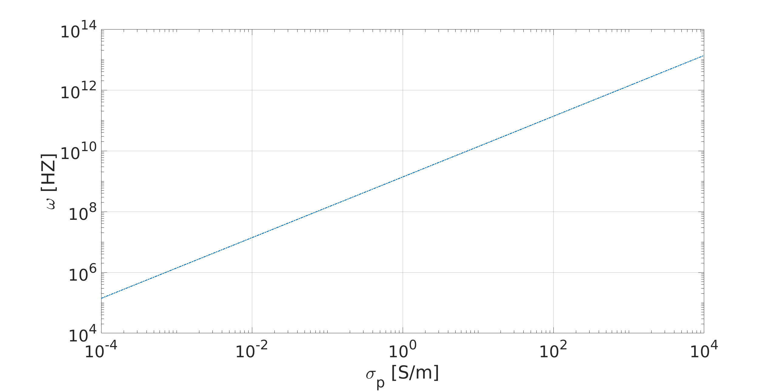
This means that the frequency of zero force shifts to the right with the increment in the conductivity of particle so to absorb SWCNTs with lower conductivity (wide-bandgap) we should go to lower frequencies and vice versa. Figure 1 shows the dependency of the frequency to varying between and .
3 Ellipsoid particle model of CNTs
We now use a more realistic model namely, prolate ellipsoid, to find the right interval for the frequency of applied voltage. In [37], an ellipsoid particle model in an electric field was introduced. The model predicts the potential at the ellipsoid’s surface leading to the induced dipole moment. In this section, we strive to introduce the ellipsoid model of nanotubes to find proper frequency intervals of the applied electric field to absorb semiconductor nanotubes and compare the result to the prevalent model (sphere model). In other words, the main goal is to show that the ellipsoid model is better suited to model cylindrical shape nanotubes, and by using this model we can find a better estimate of the frequency interval of the applied electric field to absorb semiconductor carbon nanotubes.
The problem of the ellipsoid in an electric field can be solved by introducing elliptical coordinates [38]. We should note that in the case of an SWCNT, we have different permittivities and conductivities in different directions. In the case of semiconductors, SWCNT’s longitudinal polarizability factor typically is more than ten times higher than transverse polarizability [39]. Furthermore, these dipoles generated in the middle part cancel each other pairwise so we have a high aspect ratio, i.e., a high length to radios ratio for the generated dipole.
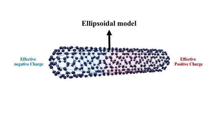
Figure 2 illustrates the general idea of the ellipsoid model for the SWCNT dipole. In an external electric field, all atoms get polarized and those atoms located near each other overlap with each other and we get two main centers for two opposite charge the positive one in the leftmost side and a negative one in the rightmost side so we have a dipole with a characteristic length as the length of the SWCNTs.
The resulting equation for the induced dipole moment in the direction is
| (19) |
where is depolarization factor for the axis
| (20) |
Where , , and are half length along the axes and is the complex permittivity in the direction . Comparing equation (10) to (19), we conclude that in this case for Clausius-Mossotti factor we have
| (21) |
If , all three s are so we get the same result for Clausius-Mossotti factor as before for sphere. If that we are concerned, s can be calculated as follows
| (22) |
where is the eccentricity and is defined as follows
| (23) |
For very long needle-shaped ellipsoid we have following approximation for
| (24) |
For and we get
| (25) |
In the case of a SWCNT with diameter to length ratio of (which is relevant in our case) we have and . From equation (19) and (2) we get the following formula for the time averaged force exerted on a SWCNT in this model
| (26) |
As before we need real and imaginary parts of Clausius-Mossotti factor which in this case from equation (26) we get
| (27) | ||||
| (28) |
The relaxation time constant for each directions in this case is
| (29) |
The point here is that an ellipsoid particle in an electric field always aligns itself with its longest axes along the direction of electric field so in this case, the ruling term is .
In the case of a long SWCNT with a high aspect ratio, we get the following approximate formula for the experienced force by SWCNT
| (30) |
where is the longitudinal complex permittivity. Frequency dependence of the force is present in the term. With this approximation we have following range of the applied frequency:
| (31) |
where the right hand side indicates
| (32) |
| parameter | |||||||
|---|---|---|---|---|---|---|---|
| value | 30 | 0 |
In order to estimate the frequency, we use the efficient parameters, summarized in Table 1. Accordingly we get
| (33) |
Here like Eq. 18, with increasing electrical conductivity of SWCNTs, frequency of zero force shift to the right and also relaxation time constant increases so to absorb SWCNTs with higher electrical conductivity we should use higher frequencies which results in absorption of more metal SWCNTs and as a result fabricated device shows metallic behavior. besides that, because of the presence of other forces that result in different motions like electro thermal motion or Brownian motion we should choose the frequency near the lower limit to have higher DEP force and near the stable polarization.
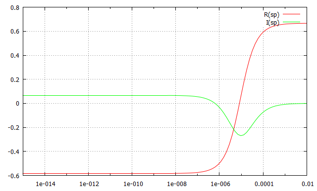
An important point here is that the transverse conductivity of SWCNT is much lower than its longitudinal conductivity and consequently we assume it to be zero. Figure 3 shows that variation in this assumption has not a considerable effect on the real and imaginary part of the Clausius-Mossotti factor. According to Figure 3 variation in is restricted to the interval and for I restricted to the interval so totally is restricted to and to which are not comparable to longitudinal factors at the relevant frequency.
The point here is that, because of the presence of other forces which result in different motions like electrothermal motion or Brownian motion we should choose the frequency near the lower limit to have higher DEP force and near the stable polarization.
4 Experimental results
In order to identify the type (metallic or semiconductor) of aligned SWCNTs with two different applied frequencies, based on the two models, we plot I-V characteristics of fabricated devices. We know that for metallic SWCNTs we would observe a straight line in the I-V plane and for semiconductor SWCNTs we expect a nonlinear relationship between current and applied voltage. Indeed, for fabricated devices with a dominant number of semiconductor SWCNTs, with the increment in voltage more and more holes participate in the current generation and we would see an exponential I-V characteristic.
The SWCNTs used in our experiment are in the form of aqueous solution and purchased from Nanointegris (http://www.nanointegris.com/) specification for the SWNTs solution are: diameter range from to , length range varies between and 5 microns, metal catalyst impurity < 1%, amorphous carbon impurity 1-5%, electronic enrichment 98% semiconductor SWCNT. We diluted the solution to and used in the DEP process.
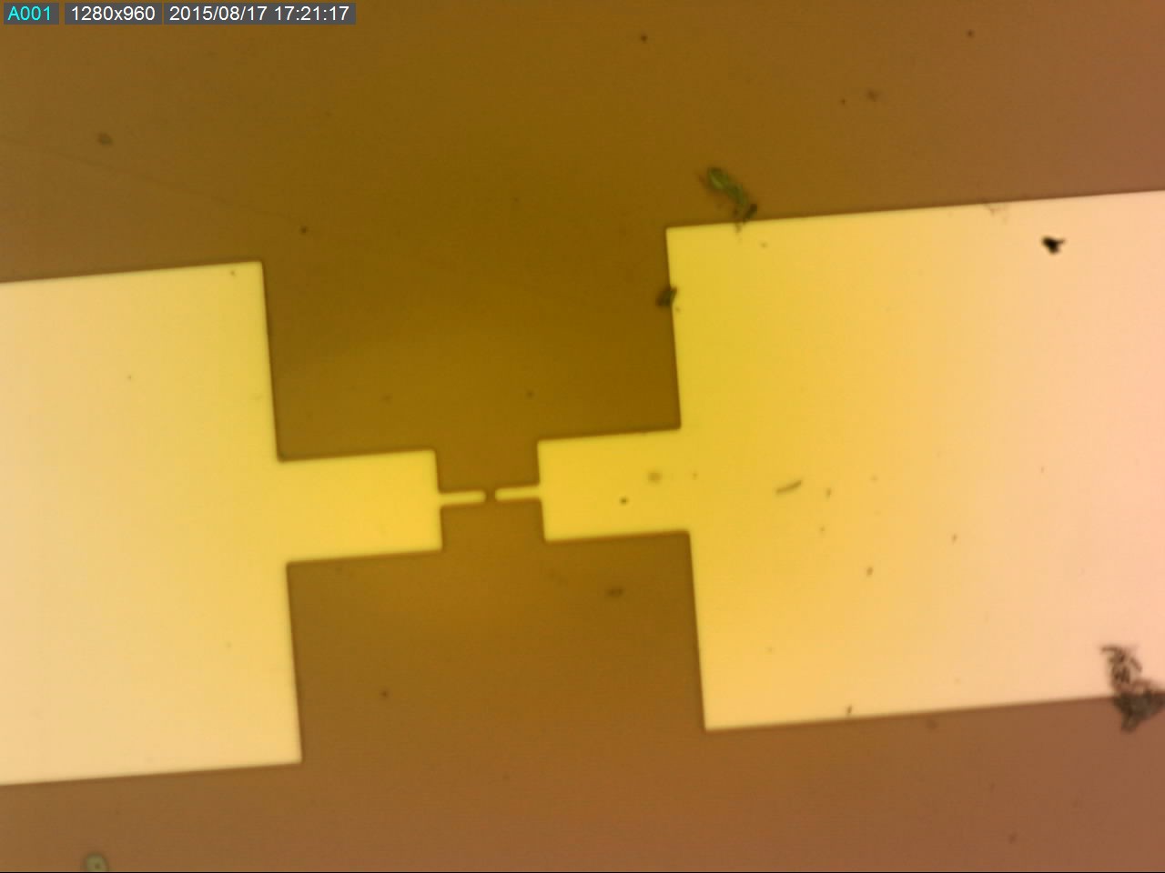
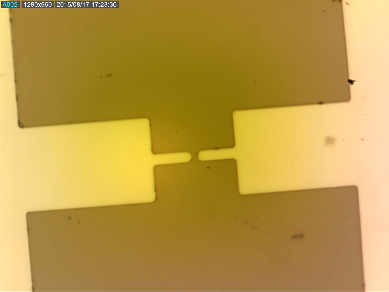
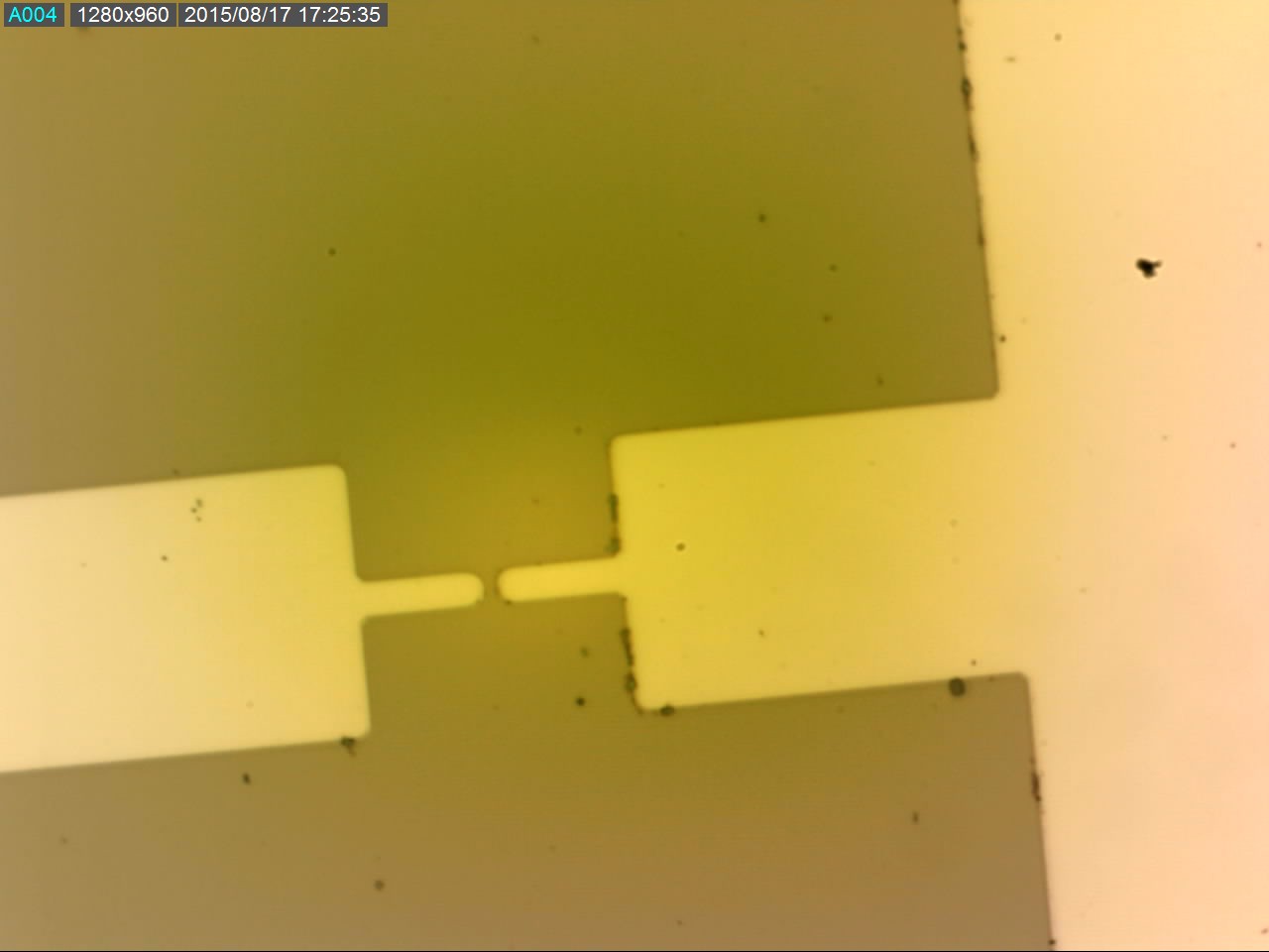
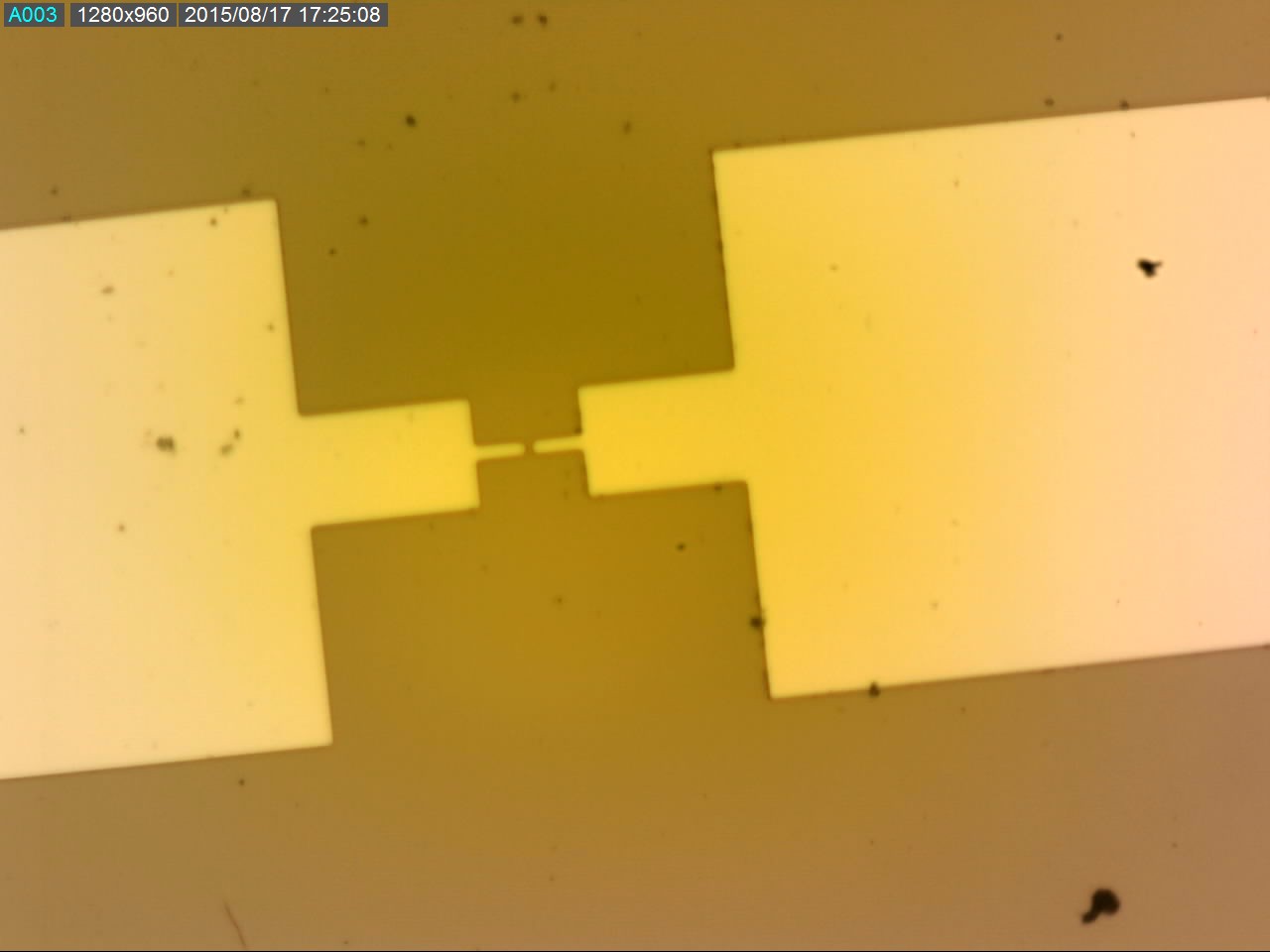
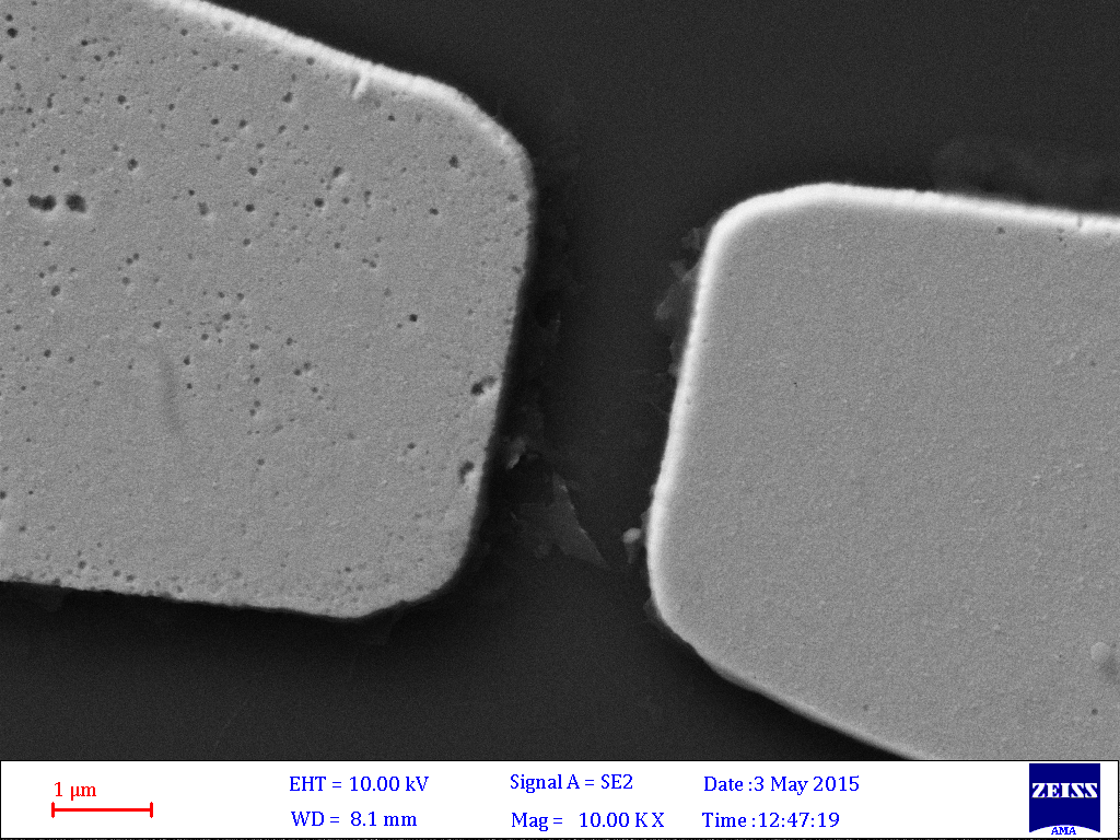
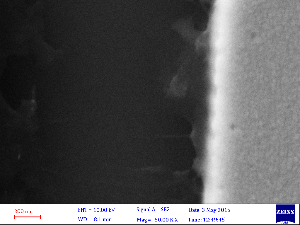
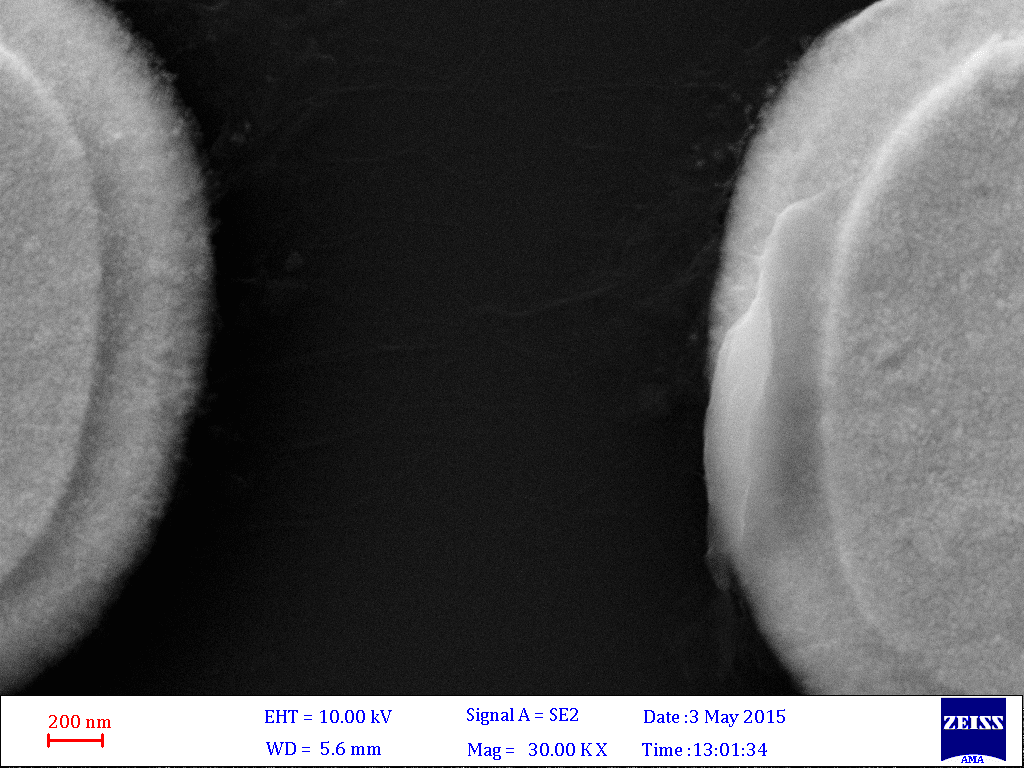
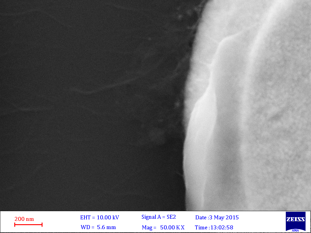
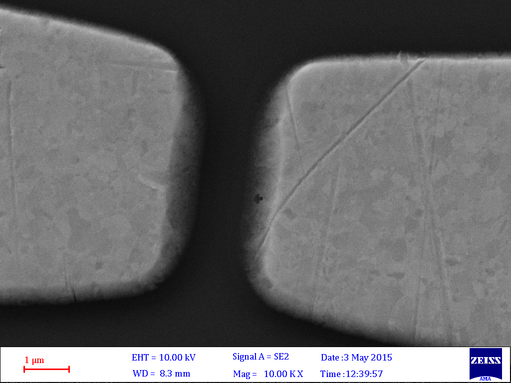
For the source and drain electrodes, we used two kinds of electrodes one with 2-microns gap and another with a 1-micron gap between electrodes both with 3-microns width at the end tip. The electrodes are shown in Figure 4.
We performed the DEP process and in order to align the SWCNTs between the electrodes an applied voltage of amplitude for 2 microns gap electrodes and for the 1-micron gap is applied.
Now we strive to use the obtained theoretical results (estimated frequencies) to align the SWCNTs. The prevalent model (sphere model) suggests that to absorb semiconductor carbon nanotubes with given parameters, we should use an AC electric field with a frequency near . The second model (ellipsoid) suggests using frequency as low as . In the experiment we will use .
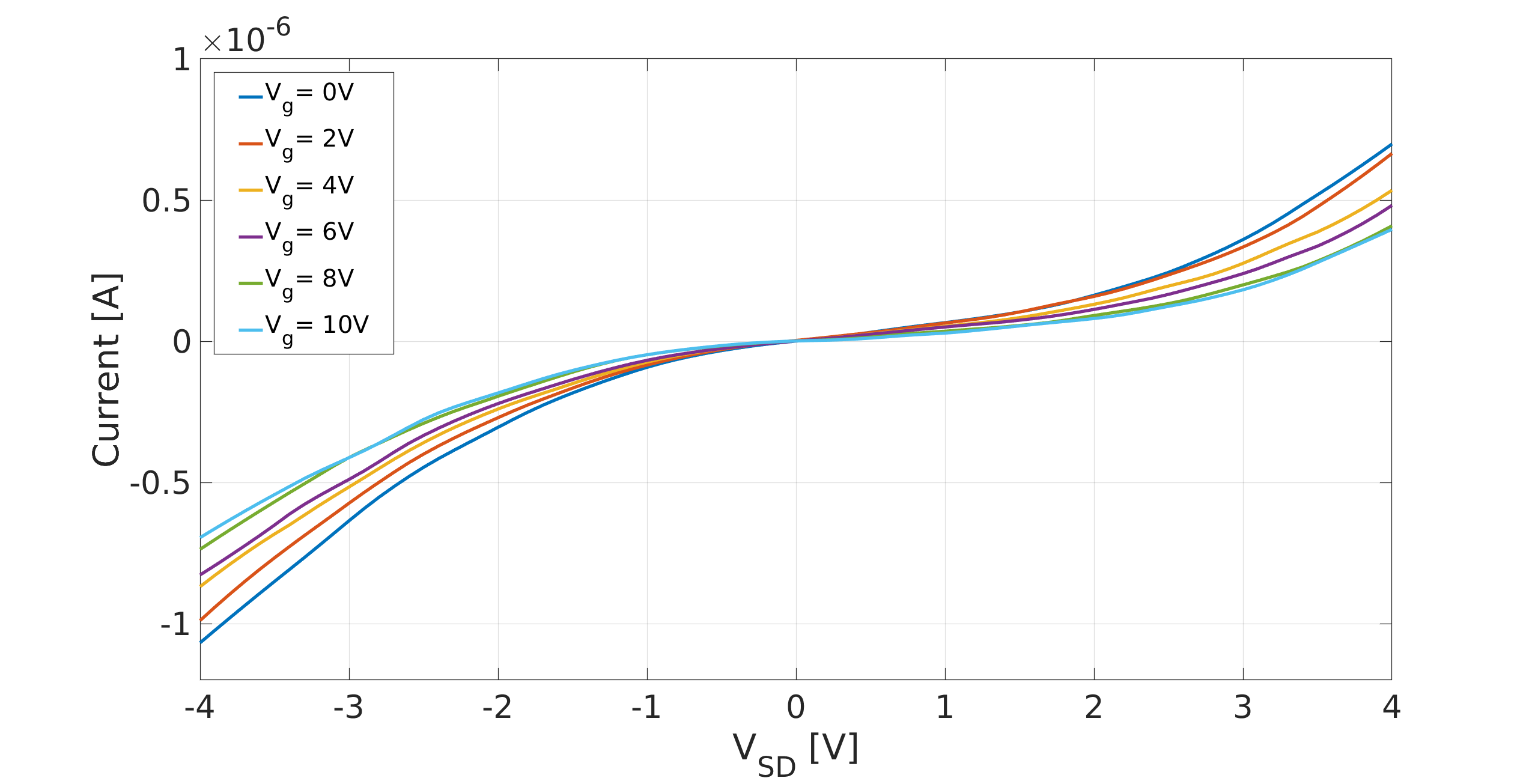
The duration of the DEP process in all experiments was 20 seconds. Figure 5 and Figure 6 show the I-V curve of SWCNTs, respectively with 1 and 2-micron gap electrodes as a function of different source-to-drain voltages. Here, the curves are related to the different gate voltage. High linearity of curves shows that most deposited CNT(s) are metallic (low bandgap semiconductor) [40]. Figure 7 and Figure 8 show the current for several and voltages in two different fabricated devices with 2 micron gap electrodes with frequency. Here, the deviation from linearity shows that aligned SWCNT(s) are semiconductor [41].
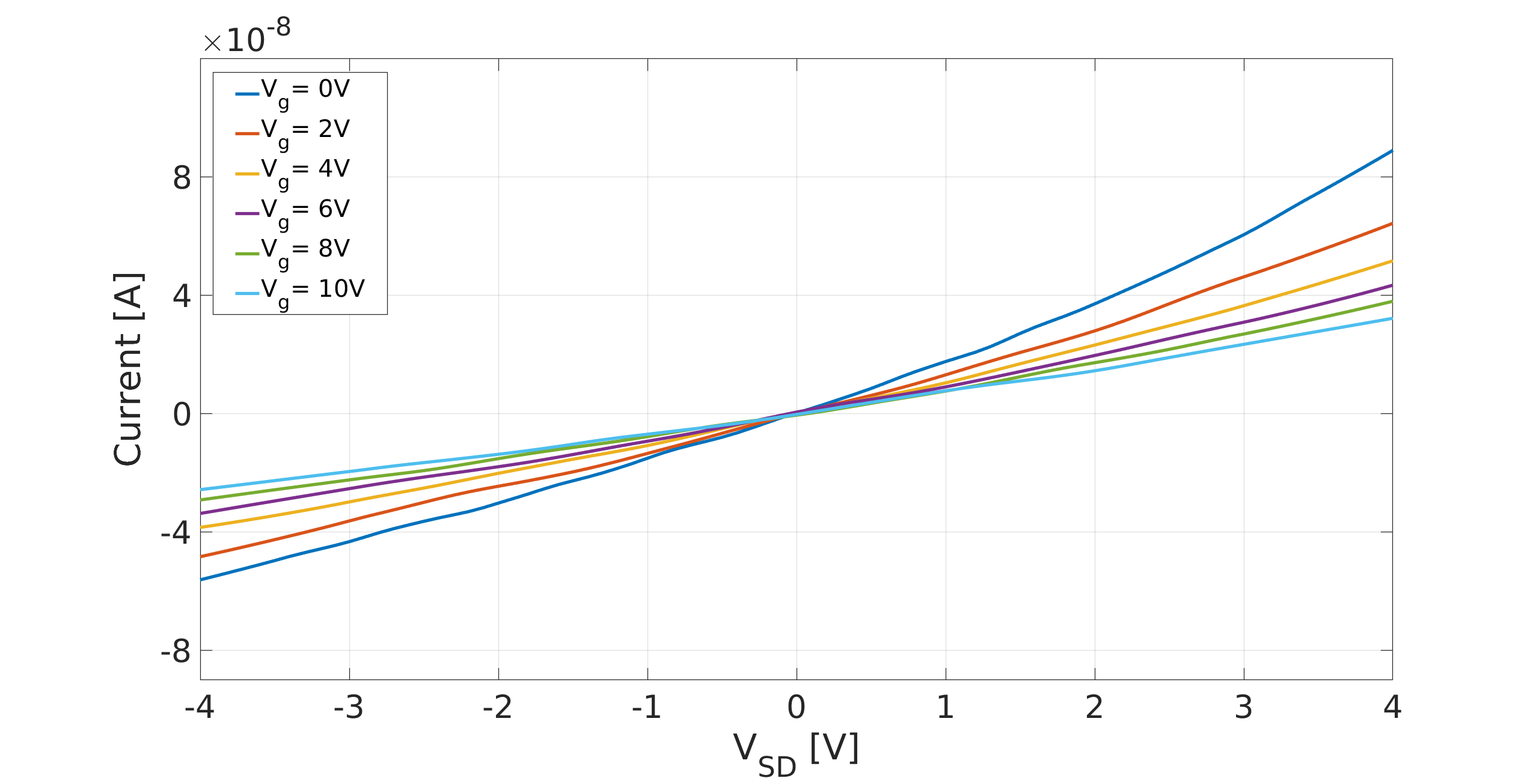
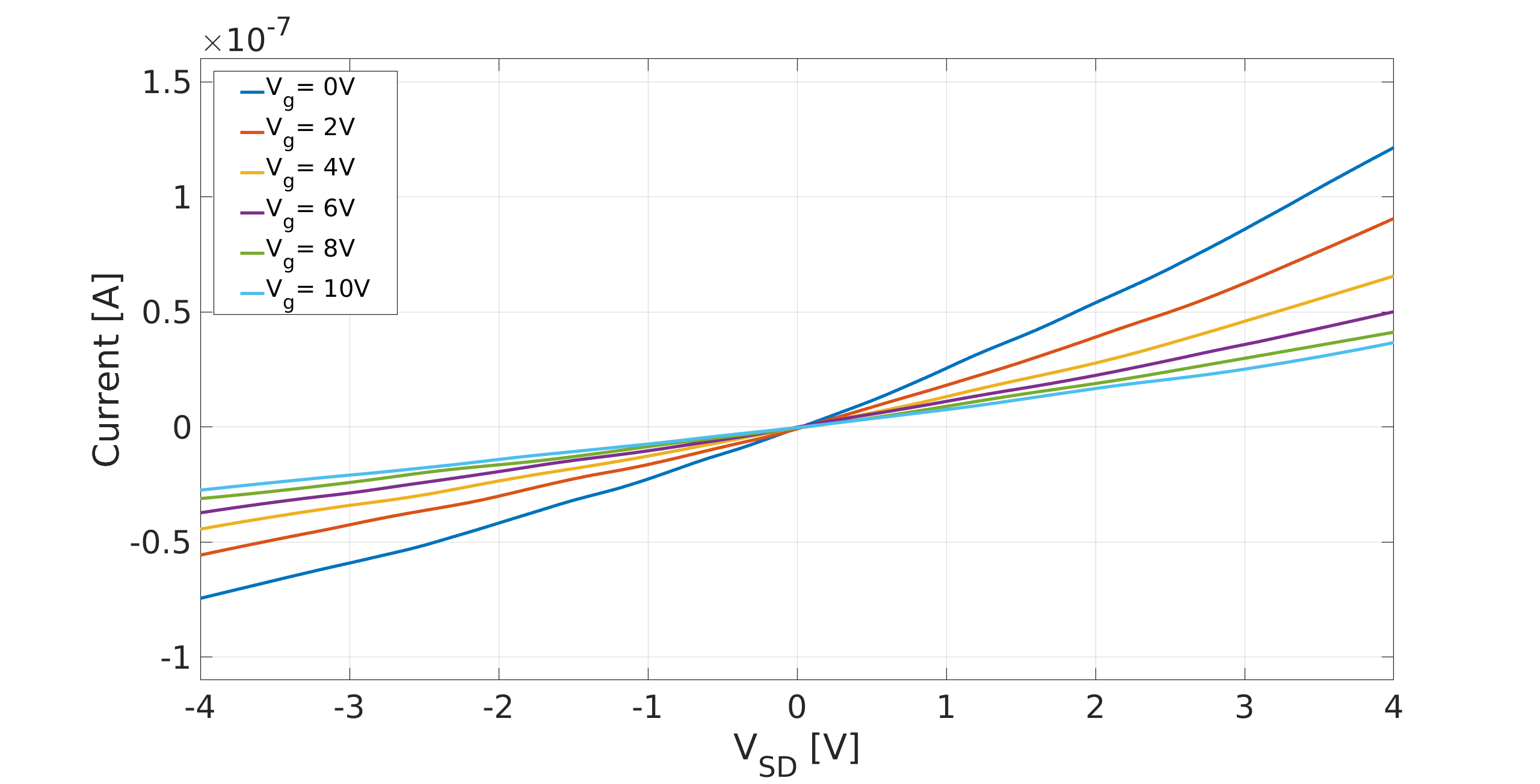
An important point to notice is that our model is just for a single SWCNT but experimental results are I-V characteristic of SWCNT bundles so we see a back gate response in I-V curves and very little deviation beginning at high source-drain voltage. In this frequency interval, we align bundles of metallic semiconductor SWCNTs with dominant metallic (low bandgap semiconductor) behavior. In fact, high linearity of curves shows that most deposited CNT(s) are metallic.
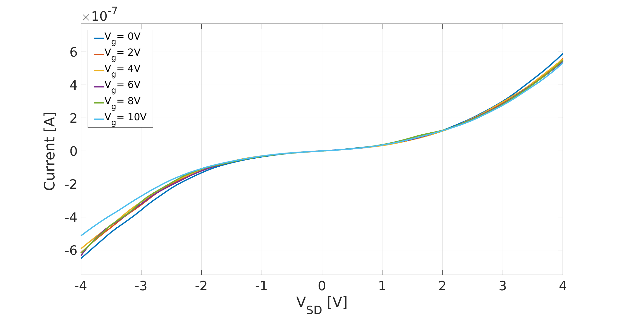
Here, we take the I-V characteristics of the SWCNT-FET into account in terms of linearity. In the case of semiconductor, intrinsic, p-type or n-type, free of external voltage, thermal agitations of electrons in the valance band causes a continues creation of electron-hole pairs i.e. electrons move from valence band to conduction band with a lifetime and result is a a constant concentration of free electrons and holes at a constant temperature. Now using SWCNT as a channel in a CNT-FET, the shape of the current-voltage characteristic is strongly affected by the potential profile across the channel [42]. Using a self-consistent field method with increasing source-drain voltage we get more states available for conduction and higher electron (hole) density in the conduction band in the case of a semiconductor so increasing external voltage we get an increasing concentration of electrons and holes (up to a point which is not present in our curves) and consequently continues increase in conductivity which results in the deviation from linearity in the case of semiconductor SWCNTs [42].
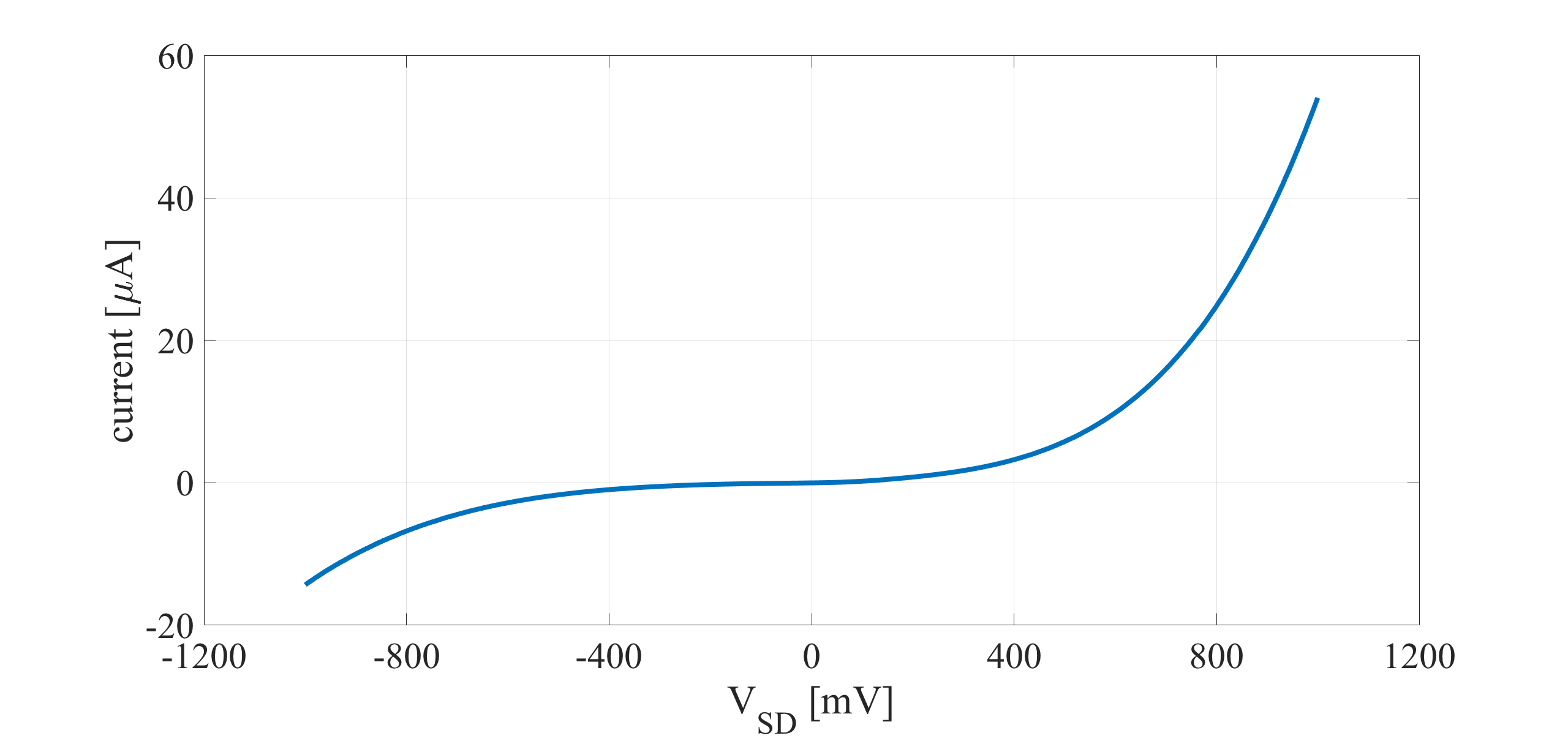
Asymmetry apparent in the curves originates from different Ohmic contacts of SWCNTs with metallic electrodes at two endpoints. As Figure 9 shows with a symmetric voltage applied the resulting I-V curve is not a symmetric one which as stated is because of different contacts at the two endpoints.
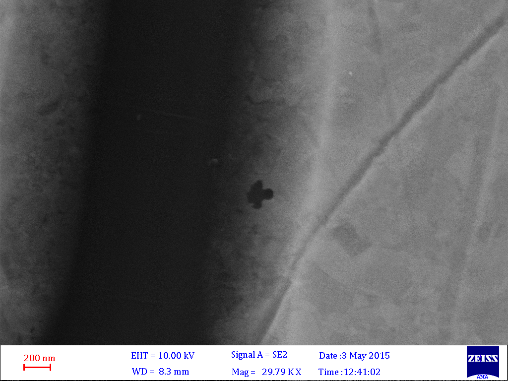
4.1 The SEM images
Here we bring scanning electron microscope images of some fabricated devices. On the right side pictures, some ropes of carbon nanotubes consisting of one or more single-walled carbon nanotubes are apparent. Another point worth mentioning is the different currents at the same voltage in I-V characteristic curves of fabricated devices which seems to be because of the different number of SWCNTs aligned between electrodes in different devices.
5 Conclusions
Experimental results show that the right frequency interval in the DEP process for alignment of single-walled carbon nanotubes is the one suggested by the ellipsoid model and in the case of large gap semiconductor SWCNTs shows a great difference; two orders of magnitude; with a spherical model which is prevalent in the articles. Picking the right frequency interval, as the theoretical model suggests, adjusting other parameters of the process such as the geometry of electrodes and changing the metal electrodes we can fully realize a more effective carbon nanotube field-effect transistor based on the DEP process. It is also well depicted that, choosing the right parameters, dielectrophoresis can be applied as a reliable way for carbon nanotube FET fabrication on a large scale.
6 Acknowledgments
A. Khodadadian and C. Heitzinger acknowledge financial support given by the FWF (Austrian Science Fund) START project No. Y660 PDE Models for Nanotechnology.
References
- [1] R. Kalantari-Nejad, M. Bahrami, H. Rafii-Tabar, I. Rungger, S. Sanvito, Computational modeling of a carbon nanotube-based DNA nanosensor, Nanotechnology 21 (44) (2010) 445501.
- [2] T. Zhang, S. Mubeen, N. V. Myung, M. A. Deshusses, Recent progress in carbon nanotube-based gas sensors, Nanotechnology 19 (33) (2008) 332001.
- [3] N. Sinha, J. Ma, J. T. Yeow, Carbon nanotube-based sensors, Journal of nanoscience and nanotechnology 6 (3) (2006) 573–590.
- [4] S. Auvray, V. Derycke, M. Goffman, A. Filoramo, O. Jost, J.-P. Bourgoin, Chemical optimization of self-assembled carbon nanotube transistors, Nano Letters 5 (3) (2005) 451–455.
- [5] K. Keren, R. S. Berman, E. Buchstab, U. Sivan, E. Braun, DNA-templated carbon nanotube field-effect transistor, Science 302 (5649) (2003) 1380–1382.
- [6] G. Yu, A. Cao, C. M. Lieber, Large-area blown bubble films of aligned nanowires and carbon nanotubes, Nature nanotechnology 2 (6) (2007) 372.
- [7] X. Li, L. Zhang, X. Wang, I. Shimoyama, X. Sun, W.-S. Seo, H. Dai, Langmuir- Blodgett assembly of densely aligned single-walled carbon nanotubes from bulk materials, Journal of the American Chemical Society 129 (16) (2007) 4890–4891.
- [8] S. Jin, D. Whang, M. C. McAlpine, R. S. Friedman, Y. Wu, C. M. Lieber, Scalable interconnection and integration of nanowire devices without registration, Nano Letters 4 (5) (2004) 915–919.
- [9] M. Engel, J. P. Small, M. Steiner, M. Freitag, A. A. Green, M. C. Hersam, P. Avouris, Thin film nanotube transistors based on self-assembled, aligned, semiconducting carbon nanotube arrays, ACS nano 2 (12) (2008) 2445–2452.
- [10] H. A. Pohl, The motion and precipitation of suspensoids in divergent electric fields, Journal of Applied Physics 22 (7) (1951) 869–871.
- [11] A. Vijayaraghavan, S. Blatt, D. Weissenberger, M. Oron-Carl, F. Hennrich, D. Gerthsen, H. Hahn, R. Krupke, Ultra-large-scale directed assembly of single-walled carbon nanotube devices, Nano letters 7 (6) (2007) 1556–1560.
- [12] P. Stokes, S. I. Khondaker, High quality solution processed carbon nanotube transistors assembled by dielectrophoresis, Applied Physics Letters 96 (8) (2010) 083110.
- [13] L. An, C. Friedrich, Dielectrophoretic assembly of carbon nanotubes and stability analysis, Progress in Natural Science: Materials International 23 (4) (2013) 367–373.
- [14] P.-F. Wu, G.-B. Lee, Assembly of carbon nanotubes between electrodes by utilizing optically induced dielectrophoresis and dielectrophoresis, Advances in OptoElectronics 2011 (2011).
- [15] A. Vijayaraghavan, Bottom-up assembly of nano-carbon devices by dielectrophoresis, physica status solidi (b) 250 (12) (2013) 2505–2517.
- [16] A. Abdulhameed, I. Abdul Halin, M. N. Mohtar, M. N. Hamidon, The role of medium on the assembly of carbon nanotube by dielectrophoresis, Journal of Dispersion Science and Technology (2019) 1–12.
- [17] N. Xi, K. Lai, Nano optoelectronic sensors and devices: nanophotonics from design to manufacturing, William Andrew, 2011.
- [18] M. Abbaszade, M. Mohebbi, Fourth-order numerical solution of a fractional PDE with the nonlinear source term in the electroanalytical chemistry, Iranian Journal of Mathematical Chemistry 3 (2) (2012) 195–220.
- [19] M. Abbaszadeh, Error estimate of second-order finite difference scheme for solving the Riesz space distributed-order diffusion equation, Applied Mathematics Letters 88 (2019) 179–185.
- [20] M. Dehghan, M. Abbaszadeh, Error analysis and numerical simulation of magnetohydrodynamics (MHD) equation based on the interpolating element free galerkin (IEFG) method, Applied Numerical Mathematics 137 (2019) 252–273.
- [21] M. Dehghan, M. Abbaszadeh, An efficient technique based on finite difference/finite element method for solution of two-dimensional space/multi-time fractional Bloch–Torrey equations, Applied Numerical Mathematics 131 (2018) 190–206.
- [22] M. Dehghan, Finite difference procedures for solving a problem arising in modeling and design of certain optoelectronic devices, Mathematics and Computers in Simulation 71 (1) (2006) 16–30.
- [23] M. Dehghan, M. Abbaszadeh, A. Mohebbi, Legendre spectral element method for solving time fractional modified anomalous sub-diffusion equation, Applied Mathematical Modelling 40 (5-6) (2016) 3635–3654.
- [24] A. Khodadadian, M. Parvizi, M. Abbaszadeh, M. Dehghan, C. Heitzinger, A multilevel Monte Carlo finite element method for the stochastic Cahn–Hilliard–Cook equation, Computational Mechanics 64 (4) (2019) 937–949.
- [25] M. Dehghan, On the solution of an initial-boundary value problem that combines neumann and integral condition for the wave equation, Numerical Methods for Partial Differential Equations: An International Journal 21 (1) (2005) 24–40.
- [26] V. Mohammadi, M. Dehghan, A. Khodadadian, T. Wick, Numerical investigation on the transport equation in spherical coordinates via generalized moving least squares and moving kriging least squares approximations, Engineering with Computers (2019) 1–19doi:https://doi.org/10.1007/s00366-019-00881-3.
- [27] A. Khodadadian, C. Heitzinger, Basis adaptation for the stochastic nonlinear Poisson–Boltzmann equation, Journal of Computational Electronics 15 (4) (2016) 1393–1406.
- [28] S. Mirsian, A. Khodadadian, M. Hedayati, A. Manzour-ol Ajdad, R. Kalantarinejad, C. Heitzinger, A new method for selective functionalization of silicon nanowire sensors and Bayesian inversion for its parameters, Biosensors and Bioelectronics 142 (2019) 111527.
- [29] A. Khodadadian, K. Hosseini, A. Manzour-ol Ajdad, M. Hedayati, R. Kalantarinejad, C. Heitzinger, Optimal design of nanowire field-effect troponin sensors, Computers in biology and medicine 87 (2017) 46–56.
- [30] A. Khodadadian, L. Taghizadeh, C. Heitzinger, Three-dimensional optimal multi-level Monte–Carlo approximation of the stochastic drift–diffusion–Poisson system in nanoscale devices, Journal of Computational Electronics 17 (1) (2018) 76–89.
- [31] A. Khodadadian, B. Stadlbauer, C. Heitzinger, Bayesian inversion for nanowire field-effect sensors, Journal of Computational Electronics 19 (1) (2020) 147–159.
- [32] A. Khodadadian, L. Taghizadeh, C. Heitzinger, Optimal multilevel randomized quasi-Monte-Carlo method for the stochastic drift–diffusion-Poisson system, Computer Methods in Applied Mechanics and Engineering 329 (2018) 480–497.
- [33] A. Khodadadian, M. Parvizi, C. Heitzinger, An adaptive multilevel Monte Carlo algorithm for the stochastic drift–diffusion–Poisson system, Computer Methods in Applied Mechanics and Engineering 368 (2020) 113163.
- [34] A. Khodadadian, C. Heitzinger, A transport equation for confined structures applied to the OprP, Gramicidin A, and KcsA channels, Journal of Computational Electronics 14 (2) (2015) 524–532.
- [35] M. H. Nayfeh, M. K. Brussel, Electricity and magnetism, Courier Dover Publications, 2015.
- [36] R. R. Pethig, Dielectrophoresis: Theory, methodology and biological applications, John Wiley & Sons, 2017.
- [37] J. Gimsa, A comprehensive approach to electro-orientation, electrodeformation, dielectrophoresis, and electrorotation of ellipsoidal particles and biological cells, Bioelectrochemistry 54 (1) (2001) 23–31.
- [38] L. D. Landau, J. Bell, M. Kearsley, L. Pitaevskii, E. Lifshitz, J. Sykes, Electrodynamics of continuous media, Vol. 8, Pergamon Press, 2013.
- [39] B. Kozinsky, N. Marzari, Static dielectric properties of carbon nanotubes from first principles, Physical review letters 96 (16) (2006) 166801.
- [40] W. Xue, P. Li, Dielectrophoretic deposition and alignment of carbon nanotubes, Carbon Nanotubes-Synthesis, Characterization, Applications (2011) 171–190.
- [41] P. G. Collins, H. Bando, A. Zettl, Nanoscale electronic devices on carbon nanotubes, Nanotechnology 9 (3) (1998) 153.
- [42] S. Datta, Quantum transport: atom to transistor, Cambridge University Press, 2005.