Strong Localization Effects in the Photoluminescence of Transition Metal Dichalcogenide Heterobilayers
Abstract
The emergence of various exciton-related effects in transition metal dichalcogenides (TMDC) and their heterostructures has inspired a significant number of studies and brought forth several possible applications. Often, standard photoluminescence (PL) with microscale lateral resolution is utilized to identify and characterize these excitonic phenomena, including interlayer excitons (IEXs). We studied the local PL signatures of van der Waals heterobilayers composed of exfoliated monolayers of the (Mo,W)(S,Se)2 TMDC family with high spatial resolution (down to 30 nm) using tip-enhanced photoluminescence (TEPL) with different orders (top/bottom) and on different substrates. We evidence that other PL signals may appear near the reported energy of the IEX transitions, possibly interfering in the interpretation of the results. While we can distinguish and confirm the presence of IEX-related PL in MoS2-WS2 and MoSe2-WSe2, we find no such feature in the MoS2-WSe2 heterobilayer in the spectral region of 1.7–1.4 eV, where the IEXs of this heterobilayer is often reported. We assign the extra signals to the PL of the individual monolayers, in which the exciton energy is altered by the local strains caused by the formation of blisters and nanobubbles, and the PL is extremely enhanced due to the decoupling of the layers. We prove that even a single nanobubble as small as 60 nm—hence not optically visible—can induce such a suspicious PL feature in the micro-PL spectrum of an otherwise flat heterobilayer.
keywords:
transition metal dichalcogenide, van der Waals heterostructure, heterobilayer, tip-enhanced photoluminescence, interlayer excitonJHI] J. Heyrovský Institute of Physical Chemistry, Czech Academy of Sciences, Dolejškova 2155/3, 182 23 Prague, Czech Republic JHI] J. Heyrovský Institute of Physical Chemistry, Czech Academy of Sciences, Dolejškova 2155/3, 182 23 Prague, Czech Republic JHI] J. Heyrovský Institute of Physical Chemistry, Czech Academy of Sciences, Dolejškova 2155/3, 182 23 Prague, Czech Republic
The fabrication of two-dimensional (2D) materials by stacking different layered materials on top of each other has attracted the attention of the scientific community due to the unique properties and the potential implementation options of the thus created van der Waals heterostructures in several optoelectronic devices, such as photodetectors, light-emitting diodes, or lasers.1, 2, 3, 4, 5, 6, 7 The understanding of the fundamental aspects that govern the properties of these systems is essential for the development of the targeted applications. Among 2D materials, transition metal (Mo, W) dichalcogenides (S, Se) (TMDCs) have emerged as research topics because of their semiconductor nature with direct bandgap energy in the visible region at the monolayer limit.8, 9, 10 Heterobilayers fabricated by the stacking of different monolayers exhibit strong interlayer coupling in a type-II band alignment and potentially a radiative recombination of interlayer excitons (IEXs) when the photoexcited electron and hole are localized in separate layers.11 IEXs formed in TMDC heterobilayers possess unique properties, such as high binding energies, long radiative lifetimes, electrical tunability, and valley polarization, which allows the excitation of either electrons or holes in a particular valley using circularly polarized light.12, 13, 14, 15, 16
Experimentally, IEX emissions have been detected at room temperature by using -photoluminescence (-PL) in several combinations of TMDCs. For example, the IEX emissions have been observed in MoS2-WS2 and MoS2-WSe2 in the energy range between 1.4–1.6 eV and 1.3–1.4 eV, respectively.17, 18, 19, 20, 21, 22, 23, 24 The MoS2-WSe2 heterobilayer presents a special case due to the large lattice mismatch and the offset of energy levels.25 The IEX in MoS2-WSe2 was reported to appear at energies between 1.6–1.55 eV, and it was assigned to the momentum-space indirect interlayer emission.26, 27 For this system, Fang et al.28 first reported the IEX at 1.55 eV, while Kunstmann et al.26 reported similar PL features at 1.6 eV. Although SiO2 substrates were used in both studies, the samples differed in the dry transfer technique. In the former work,28 the exfoliated monolayers were picked up from the substrate with polydimethylsiloxane (PDMS), whereas the monolayers were exfoliated directly on PDMS in the latter work.26 Several researchers have reported similar PL features in samples prepared by a variety of methods, for example, using PDMS stamps for transferring only the top layer, or after encapsulating the layer with hBN, or even when using a wet transfer method, all in the energy range of 1.6–1.5 eV.29, 30, 31, 32 However, a few recent authors have argued the presence of the MoS2-WSe2 space indirect interlayer emission further in the infrared region, at 1.1 eV.33, 34
Despite reported observations of interlayer emissions in various systems by conventional –PL methods, studies of local PL signatures and the effects of heterogeneities on the interaction between the layers are lacking. This is particularly important when preparing heterobilayers by other means than direct growth. In manually stacked heterostructures, the formation of various out-of-plane features is unavoidable, in part due to contamination and in part due to deformation induced by the handling. Often, the resulting topography imperfections cannot be spotted in the diffraction limit, be it optical microscopy or spectroscopy. 35, 36 In previous works, tip-enhanced photoluminescence (TEPL) has been utilized to probe local nanoscale heterogeneities in different TMDC monolayers.37, 38, 39, 40, 41 Herein, we catalogue the local PL signatures of variously stacked TMDC heterobilayers and confirm the presence of interlayer emission from the flat parts of MoS2-WS2 and MoS2-MoSe2. In contrast, no interlayer emission in the range of 1.5–1.6 eV takes place in WSe2-MoS2 heterobilayers with stacking angles close to 0º, even in cases where a perfect interface is documented by a clear Moiré pattern in topography. We identify different surface imperfections by TEPL spectroscopy in WSe2-MoS2 heterobilayers with emission energies ranging from 1.6 eV to 1.5 eV and assign those bands to the PL of the top layer, which shifts due to the strain caused by the encapsulated contamination.
1 Results
We prepared heterobilayers by combining different mechanically exfoliated TMDC monolayers by a dry transfer method (see Experimental for details). Figure 1(a) shows the topography of a WSe2/MoS2 heterobilayer on SiO2/Si, illustrating the typical heterogeneities introduced by the stacking of 2D materials. Note that throughout the text, the heterobilayers are always designated as A/B, where A is the top layer and B the bottom one. If the heterobilayer is labeled as A-B, we do not make a distinction of the layer order. Besides small bubbles created in the bottom layer (MoS2), the topography is dominated by the formation of blisters in the top layer (WSe2) due to the lateral diffusion of contamination, leading to a clean interface in between the blisters.42 Otherwise, the top layer maintains the topography of the bottom layer. The PL in the heterobilayer area is strongly quenched, owing to the strong interlayer charge transfer between the two monolayers,43 as shown in Figure 1(b). The varied -PL signals within the heterobilayer area are outlined in the bottom panel of Figure 1(c), whereas the PL spectra in the top panel correspond to the individual monolayers. The heterobilayer exhibits emissions at 1.65 and 1.85 eV, corresponding to the intralayer excitons for WSe2 and MoS2, respectively. An extra band is centered at 1.6 eV, and it becomes weaker in the regions where the atomic force microscopy (AFM) topography image looks more flat. This band is within the range for the reported momentum-space indirect interlayer emission in WSe2/MoS2,26 and it might be assigned to such excitonic species. However, the limited resolution of the -PL system makes it impossible to discern between signals coming from the nano-sized features observed in the AFM image. To improve the spatial resolution of the PL map, we performed a TEPL survey in the same sample area, and the results are summarized in Figure 1(d–g). When comparing the AFM image and the TEPL map measured during the same scan, one can see that the PL signal from the blisters is stronger than the PL observed in the flat areas. Moreover, the spectra extracted from the enlarged map reveal that the PL of the blisters is redshifted by 0.05 eV with respect to the WSe2 neutral intralayer emission (Figure 1(g) and S6). This band coincides with the position of the extra band observed by –PL, and it is often assigned in the literature to the IEX.26, 28, 30, 29 We note that we did not take into consideration the twisted angle since the emission at 1.6 eV was observed for all the angles studied in the previous works.26, 27
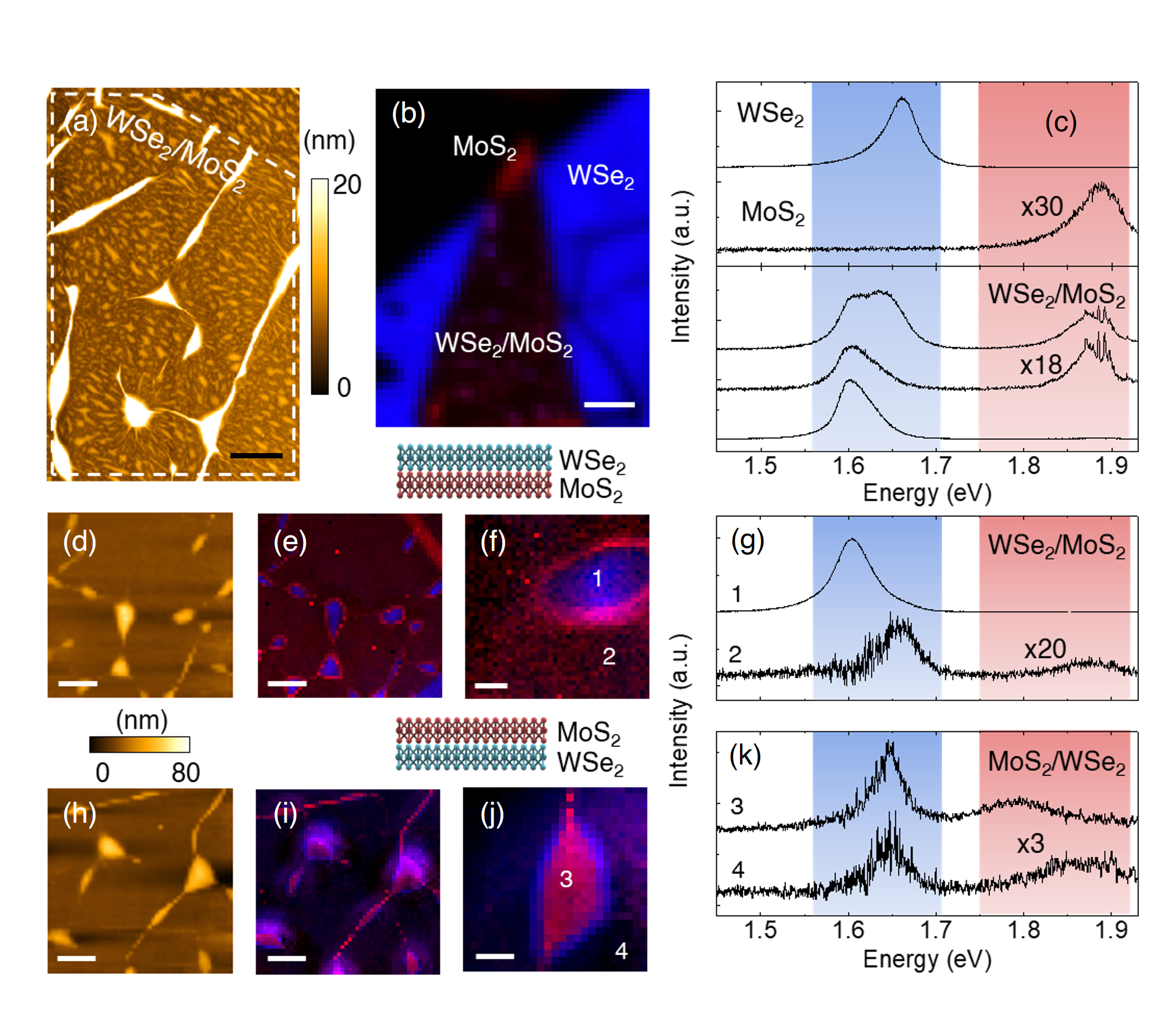
Since the TEPL from the flat areas in Figure 1(g) did not show any additional band other than the emission from the individual monolayers, we prepared samples with an inverse layer order by placing the MoS2 on top (see Figure S3 for –PL maps). In MoS2/WSe2, the TEPL map (Figure 1(h–k)) shows behavior opposite to the WSe2/MoS2 case, and now the PL signal from the blisters shifts by 0.05 eV with respect to the MoS2 intralayer emission (from 1.85 eV to 1.8 eV), while no extra band is observed at 1.6 eV. Hence, in both cases, the blisters form in the top layers, and their intrinsic PL signal redshifts while the flat areas do not show any extra bands. The more intense PL of the layers in the blisters suggests a weaker interlayer interaction takes place in those areas. We attribute the observed redshift to the strain caused by the formation of contamination pockets.44 The exact position of the emission will depend on the level of strain, in a fashion similar to the case of monolayer WS2 on a gold substrate, as reported recently.45 We point out that the PL from the small bubbles formed between the bottom TMDC monolayer and the SiO2 substrate (observed in the higher resolution AFM image in Figure 1(a)) seems to be unaffected.
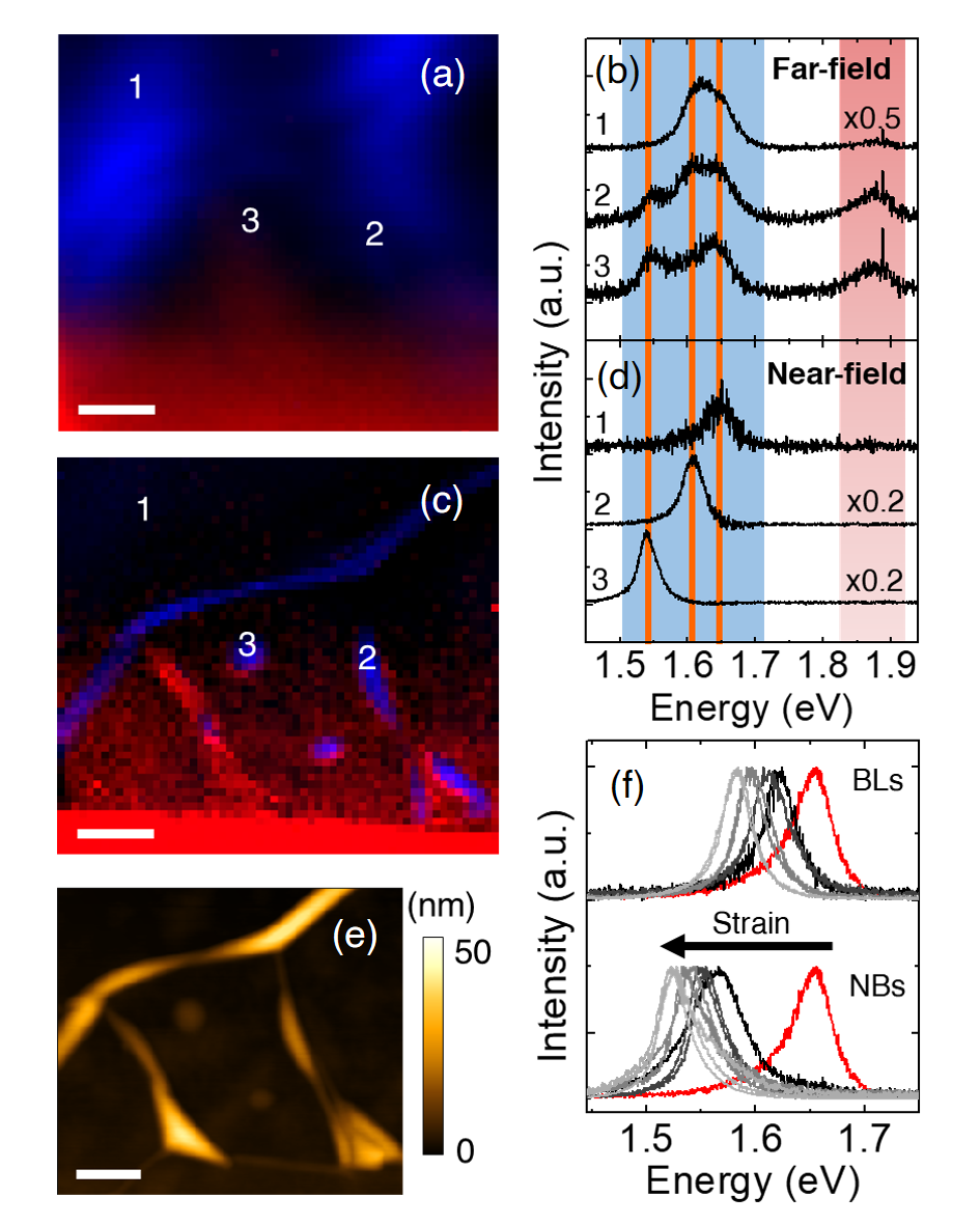
To shed more light on the possible disentanglement of local strain-induced shifts and interlayer emission (if it exists) in this particular heterobilayer, we prepared the same structure but on hexagonal boron nitride (hBN) to assess the effect of the substrate. For these samples, we expect that blisters will appear in both MoS2 and WSe2 layers, independently of the stacking order. Figure 2(a) shows the far-field PL intensity map of the heterobilayer on hBN when WSe2 is placed on top of the MoS2. The far-field here is taken with side illumination in our TEPL setup 40. As expected, a more heterogeneous PL distribution is observed due to the formation of both MoS2 and WSe2 blisters. The spectra in Figure 2(b) shows the far-field PL spectra of selected areas in the heterostructure, where different bands near the WSe2 emission of the neutral exciton can be observed. Interestingly, the spectral features acquired in the far-field can be resolved in the near-field map (Figure 2(c)). Figure 2(d) shows three different bands, making the assignment straightforward. Number one is for the intrinsic WSe2 intralayer emission at 1.65 eV, number two is similar to the previously observed band for the blisters at 1.6 eV, and number three at 1.55 eV exhibits an even larger shift. The topography image of the same sample area (Figure 2(e)) shows that the intensity of the TEPL signals correlates with the topography features observed in the AFM image. Interestingly, besides the previously described blisters (#2 in (c) and (d)), we observed another feature with a more circular shape (#3) which corresponds to the PL emission at 1.55 eV. Such features have recently been observed in WSe2/hBN heterostructures, introduced as nanobubbles, 46 and assigned to the emission from localized exciton (LX) states. We analyzed the emission energies of the various surface heterogeneities for different samples and separated them into two groups: blisters and nanobubbles (Figure 2(f)). In general, nanobubbles (1.52–1.58 eV) induce larger PL shift than blisters (1.58–1.62 eV) due to larger strain and localization. The shapes of both types indicate they are filled with gas or liquid, rather than with a nanoparticle (cf. Figure S11).47
Besides the emissions from the blisters and nanobubbles, none (e.g., from interlayer excitons) were observed in the spectra. To evaluate the effect of \sayoptically invisible nanobubbles on the resulting PL spectra, we measured a TEPL map in an area that contains no visible blisters and is large enough to be resolved with conventional –PL methods. Figure 3(a) shows a 4 4 m2 \sayflat area of the same type of heterostructure as in Figure 2 (i.e., WSe2/MoS2 on hBN). Apart from the bottom bubbles originated between the hBN layer and the SiO2 substrate, blisters are not created in that area, and the two TMDC layers are copies of the topography of the hBN, which suggests that a clean interface between MoS2 and WSe2 should be generated. The TEPL map of that area (Figure 3(b)) shows a uniform signal distribution across the area without blisters with the exception of a strong PL feature (marked with a yellow arrow) arising from a small nanobubble in the center of the area. This particular nanobubble can be identified in the AFM image (Figure 3(a). The nanobubble is notably smaller than the bottom hBN bubbles, which, however, do not provide any recognizable PL change.
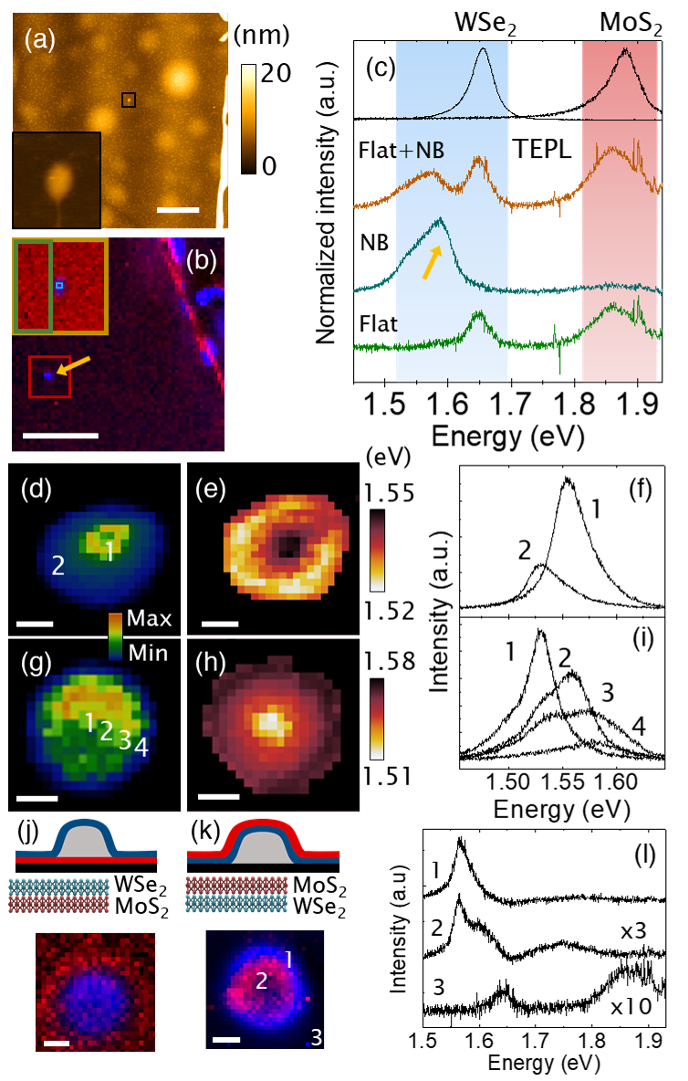
The average TEPL spectra of the areas indicated in the inset of Figure 3(b) are displayed in Figure 3(c) in the respective colors. Three bands are observed in the brown spectrum, which corresponds to the average of all the spectra in the inset. Besides the intralayer emissions at 1.65 eV and 1.85 eV for WSe2 and MoS2, respectively, an extra band is observed at 1.58 eV, which could immediately be assigned to the interlayer emission, according to the reported IEX energy in some works. Nevertheless, the high spatial resolution achieved with TEPL allowed us to resolve those bands, revealing that the emission at 1.58 eV is actually the emission from the nanobubble, while the flat areas exhibit only the MoS2 and WSe2 intralayer excitons.
Figure 3(d–i) shows the PL of different WSe2 nanobubbles (on MoS2) measured with TEPL. Since the PL is extremely enhanced in those areas, it can be nicely resolved and enables the observation of the particular doughnut-like distribution of PL as a consequence of the higher strain in the nanobubbles periphery (Figure (3(e)).48, 46 In the spectra shown in Figure 3(f), one can see the more intense, less shifted PL band coming from the center of the nanobubble, while the less intense PL band with the larger shift can be observed along the circumference. In contrast, the big nanobubble (Figure 3(h)) shows a different PL energy distribution with multiple local strain states across the nanobubble, as observed in the PL spectra (Figure 3(i)). The localized states are spread into concentric rings in the nanobubble. The periphery is now dominated by higher energy states due to a weaker confinement potential in those regions. The non-trivial shape of spectrum 1 in Figure 3(i) suggests that an even better lateral resolution would be needed to fully resolve the varying localized strain states. The multitude of relatively sharp emissions from the nanobubble supports the idea of a strong relation between these heterogeneities and quantum emitters observed in WSe2,49, 50, 51, 52 as suggested by Darlington et al.46
An interesting effect occurs when placing an extra layer on top of a WSe2 nanobubble or blister, as in MoS2/WSe2 heterobilayers. Figure 3(j–k) shows the TEPL intensity map of nanobubbles for the two main configurations encountered in this work. As previously shown (Figure 2), when the WSe2 monolayer is on top, the PL from the WSe2 nanobubble is redshifted (Figures 2(d) and 2(f)) and the PL signal of MoS2 does not shift, but it is more intense in the areas immediately surrounding the nanobubble. When a MoS2 layer is placed on top of WSe2, the distribution of the PL intensity changes, exhibiting a higher PL intensity at the periphery. The \saybottom WSe2 nanobubble (i.e., below the MoS2 layer) is disturbed by the top layer modifying the strain distribution. In the center of the nanobubble, both layers exhibit strain-induced PL shifts (spectrum 2 in Figure 3(l)); however, the PL band of WSe2 is now less shifted, but weaker and broader, similarly to the effects observed in the big nanobubbles. We highlight the importance of the layer order-dependent nanobubble strain since the thus induced difference in PL shifts can be entangled with possible charge-doping effects if IEX emission is present.31
We also noticed a considerable difference between nanobubbles formed in MoS2 and WSe2 monolayers. When comparing nanobubbles of the same size and on the same substrate (e.g., on hBN), thereby assuming similar strain levels reached in the nanobubble, the TEPL signal of MoS2 is weak and the PL shift is similar to that observed in the MoS2 blisters with a much wider spectral line shape (Figure S8). Moreover, we measured larger PL shifts for nanobubbles in WSe2 (up to 150 meV with respect to the neutral excitons) than in MoS2. This is consistent with the assignment of the emission from the nanobubble to LX states, since localized states in MoS2 are observed as a broad PL band, while localized states in WSe2 exhibit a series of sharp bands. 53, 54, 55
Concerning the blisters, where the shift seems to be universal for all studied heterobilayers, it is plausible that the shift is also a consequence of strain. The assignment of the bands to different excitonic species can be more ambiguous. For WSe2, dark exciton emission was observed at 1.6 eV,56 matching well with the energies at which we observed the emission of the blisters. However, the dark excitons were observed when using Au as a substrate, forming a nano-cavity responsible for the enhanced emission. In our samples, it appears unlikely that dark excitons can be observed in the strained areas at room temperature.57 We also exclude the trion as being responsible for the measured low-energy band because the shift of the band is notably larger than the reported energy difference between the trion and neutral exciton emissions.58
To assess if the absence of measurable IEX emission in MoS2-WSe2 heterobilayers (regardless of order) is due to our sample preparation method, we prepared heterobilayers of different systems, such as MoS2-WS2 and MoSe2-WSe2 on SiO2/Si substrates (Figure 4) using the same assembly method. Figure 4 (a–d) shows the -PL spectra obtained in both samples when placing the MoX2 layer on top. Both intralayer and interlayer excitons can be observed, consistent with previous reports.18, 17, 19, 20, 21, 24, 22, 23
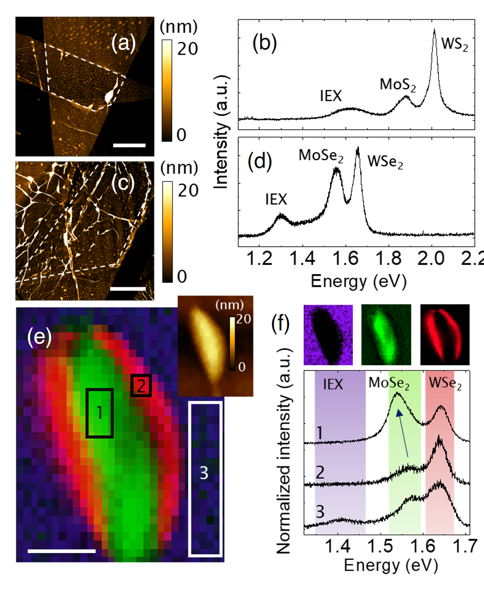
We also observed interlayer emission when placing the WX2 layer on top (Figures S4 and S5). Again, the large PL shifts caused by the blisters and nanobubbles produce characteristic shapes in the spectra. Figure 4(e–f) shows the TEPL map of a blister created in a MoSe2/WSe2 heterobilayer. The color map in Figure 4(e) shows the integrated intensity for different energy ranges indicated in Figure 4(f). Similarly to the MoS2/WSe2 heterobilayer, the PL from the blister exhibits a strain-dependent redshift of the neutral exciton from the top layer (green range), while the PL of the bottom layer is more intense in the blister surroundings (red). The PL band of the IEX can only be observed in the flat areas (magenta) due to the strong interaction between the layers.
Once we had excluded our sample preparation method as the reason for not detecting the IEX in MoS2-WSe2, we focused on preparing these heterobilayers with the strongest possible interlayer coupling. Figures 5(a–g) show a large clean area (4 4 m2) of two heterobilayers with MoS2 (a–c) and WSe2 (e–g) on top. The AFM images in Figures 5(b, f) show the presence of numerous bubbles; however, those are created when placing the first layer on the substrate, and they do not have any effect on the PL. The second layer copies the topography of the first one. We were able to image a Moiré pattern of small twist angles in both samples (Figures 5(c, g)) with simple scans in Peak Force Tapping mode, confirming a good interaction and clean interface between the layers.59, 60 The -PL spectra displayed in Figure 5(d) shows two almost identical curves, absent of any extra band in the reported IEX emission range. On top of that, the bands corresponding to the individual intralayer excitons are of the same energy in spite of the reversed layer order.
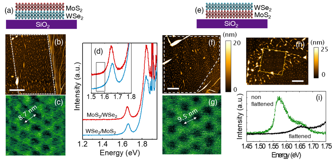
Finally, we tried to see the IEX emission in the heterobilayers both on SiO2 and hBN after removing the blisters by applying the nano-squeegee technique (scanning the area with an AFM tip in contact mode with a setpoint large enough to considerably press the sample, but small enough to avoid damaging it).61 Figures 5(h–i) show the flattened area and the corresponding PL spectra taken before and after cleaning a WSe2/MoS2 heterobilayer on SiO2. The emission at 1.6 eV completely vanishes after the removal of the blisters, confirming their responsibility for the 1.6 eV–PL band.
2 Discussion
We observed different surface imperfections with similar PL features in WSe2/MoS2 and MoS2/WSe2 heterobilayers. In general, on SiO2, only blisters are generated when the two layers are stacked, and they are distinguished by showing strong and redshifted PL of the top layer. We also detected rare protrusions caused by a nanoparticle on SiO2 when the substrates were not clean enough (Figures S11-13) that generate local strains as in the case of gas or liquid-filled blisters. On an hBN substrate, nanobubbles and blisters are created in both layers regardless on the stacking order. When WSe2 is on top, the PL of WSe2 in these protrusions exhibits larger shifts. No signatures of IEX emission in the range of 1.3–1.6 eV was observed in MoS2–WSe2 heterobilayers.
Although the electronic nature of the IEX in the different systems is still under debate, 21, 62, 63, 19, 20 we focus our discussion mostly on the MoS2-WSe2 system. While the space indirect emission has been predicted 43, 59, 34 and experimentally measured to be at energies close to 1 eV,64, 34, 33 the most common emission observed by -PL at energies between 1.55–1.6 eV was identified as a momentum-space indirect owing to the large lattice mismatch and the offset of energy levels.28, 26, 27, 29, 30, 31, 32 This particular interlayer emission was demonstrated to possess a weak twist angle dependence and became undetectable when the temperature is decreased.26
However, several factors made us consider a possible reassignment of the PL bands reported in this range.
1) The PL of the blisters and nanobubbles is much stronger than the PL of the flat areas, simply because the PL quenching is lifted due to the detachment of the layers by the encapsuled contamination, a possibility that has not been discussed in previous works. The strong PL intensity together with the strain-induced shift from these heterogeneities can influence the measurements. The lack of spatial resolution in the previous -PL studies makes the distinction between locally corrugated and flat areas almost impossible. Moreover, Huang at el. 33 recently demonstrated that the interlayer emission from MoS2–WSe2 lies at around 1 eV without any signal at around 1.6 eV.
2) The momentum-space indirect interlayer emission was demonstrated to be independent of the stacking angle between layers.26 Nevertheless, some researchers have assigned the interlayer emission at around 1.59 eV,29, 26 while others observed it at around 1.55 eV28, 31. This matches well with the measured energy for blisters and nanobubbles, respectively, with the variation being the result of different strain levels.
3) It was also demonstrated that interlayer emission disappears at low temperatures29, 26, which is unsupported by other observations in MoS2-WS2 and MoSe2-WSe2,21, 20, 19 where momentum indirect interlayer emission maintains its dependence on the temperature. However, we are aware that the lattice mismatch in MoS2/WSe2 may cause a different fundamental behavior.
4) As-grown CVD MoS2-WSe2 vertical heterobilayers are more difficult to synthesize than other vertical heterobilayers due to the high tendency to form alloys,65 and not many authors have reported the PL signature of such systems. To the best of our knowledge, only one study reported the PL of an as-grown sample, assigning the 1.6 eV-PL band as the interlayer emission.32 However, the band at 1.6 eV is broad and accompanied by redshifts of both intralayer excitons (MoS2 and WSe2), making the fitting and subsequent band assignment problematic.32 More experiments in this line of study are sorely needed.
5) In general, the position of the monolayer (MoS2 and WSe2) in the stacking order should not affect the band energy alignment.43 Yet, in our samples, the band at 1.6 eV always appears at a higher energy in MoS2/WSe2. The absence of emission at around 1.6 eV when using MoS2 as a top layer can be found in some works.66, 67 However, as discussed above, the blisters and nanobubbles that decouple the two layers provide the simultaneously enhanced and shifted PL for the top layer. Therefore, the TEPL signal of WSe2 shifts—or broadens in -PL—toward lower energies only when this particular layer is on top.
3 Conclusions
To conclude, we have investigated different combinations of heterobilayers composed of MoS2, MoSe2, WS2, and WSe2 on SiO2 and hBN, with tip-enhanced PL and high resolution AFM. We show that while MoS2-WS2 and MoSe2-WSe2 exhibit a clear signature of interlayer excitons in the energy range measured previously by PL with diffraction-limited resolution, the TEPL spectra of the MoS2-WSe2 heterostructure do not contain any clear sign of the IEX emission in the often reported energy range. Instead, we evidence PL shifts and intensity changes caused by local topography features, such as nanobubbles and blisters, which are formed between the layers due to contamination. The IEX-suspicious PL shift is absent even when the two layers exhibit a Moiré pattern, which proves a strong interaction between them. In contrast, such PL shifts take place in an optically flat sample even when a single nanobubble detectable by AFM is present. Additional effects of various nanobubble configurations on the PL spectra are described, highlighting the need for a careful interpretation of the -PL spectra of van der Waals heterostructures.
4 Methods
4.1 Sample preparation
The samples were prepared by mechanical exfoliation of bulk crystals (2D semiconductors, HQ graphene). The monolayers were separately exfoliated on polydimethylsiloxane (PDMS) stamps and transferred onto SiO2/Si substrates (300 nm SiO2) using a dry-transfer technique.68 For the samples on hBN, we first transferred 15–20 nm-thick hBN flakes onto the substrates using the same method. The temperature was set to 70° C after contacting the PMDS stamp on the substrate and cooled down before releasing the contact. The temperature facilitates the interaction between the layers and interface self-cleaning, which is evidenced by the creation of blisters. 42
4.2 Micro- and nano-photoluminescence characterization
The micro PL measurements were performed in a LabRAM HR Evolution spectrometer (Horiba Scientific) with a 633 nm laser excitation and 150 l/mm diffraction grating. The TEPL measurements were performed with the same LabRAM HR Evolution spectrometer coupled to an OmegaScope SPM (Horiba Scientific) using side-illumination with 633 nm laser excitation, 150 l/mm grating, and a 100x objective (0.7 NA). Own-made plasmonic tips were used by sputtering Ag on Si probes (Access-fm, App Nano). TEPL imaging was performed by using DualScan mode, where the AFM feedback switches from contact to semi-contact at each pixel of the scan. The emission collected when the tip is in contact contains both the near-field and far-field signals, while the far-field signal dominates the emission when the tip is in the semi-contact mode. The TEPL signal was obtained after the pixel by pixel subtraction of the far-field from the map that was collected in the contact mode (Figure S6). The applied contact force was weak (5 nN),46 as we used the minimum force needed to maintain stable feedback during the scan. The acquisition time for each pixel was 0.2–0.5 s for TEPL and 1s for -PL maps, unless specified otherwise. The -PL single spectra were collected with longer acquisition times. For all the measurements, the laser power was set between 40 and 200 W.
4.3 Topography characterization
The AFM images were taken with a Bruker Dimension ICON in PeakForce Tapping mode using Scanasyst Air probes (Bruker Corp).
This work was funded by the Czech Science Foundation (GACR 20-08633X). The study was further supported by the Pro-NanoEnviCz project (Reg. No. CZ.02.1.01/0.0/0.0/16_013/0001821) supported by the Ministry of Education, Youth and Sports of the Czech Republic and the European Union - European Structural and Investments Funds in the frame of Operational Programme Research Development and Education.
Additional -PL maps of MoS2-WSe2 heterobilayers, -PL spectra of different heterobilayers showing the IEX emission, TEPL details of MoS2-WSe2 and MoSe2/WSe2 heterobilayers, and TEPL maps of protrusions originated by nanoparticles in MoS2-WSe2 heterobilayers.
References
- Geim and Grigorieva 2013 Geim, A. K.; Grigorieva, I. V. Van der Waals Heterostructures. Nature 2013, 499, 419–425
- Novoselov et al. 2016 Novoselov, K. S.; Mishchenko, A.; Carvalho, A.; Castro Neto, A. H. 2D Materials and van der Waals Heterostructures. Science 2016, 353, aac9439
- Jariwala et al. 2016 Jariwala, D.; Marks, T. J.; Hersam, M. C. Mixed-Dimensional Van Der Waals Heterostructures. Nat. Mater. 2016, 16, 170–181
- Long et al. 2019 Long, M.; Wang, P.; Fang, H.; Hu, W. Progress, Challenges, and Opportunities for 2D Material Based Photodetectors. Adv. Funct. Mater. 2019, 29, 1803807
- Ricciardulli and Blom 2020 Ricciardulli, A. G.; Blom, P. W. M. Solution-Processable 2D Materials Applied in Light-Emitting Diodes and Solar Cells. Adv. Mater. Technol. 2020, 5, 1900972
- Liu et al. 2019 Liu, Y.; Fang, H.; Rasmita, A.; Zhou, Y.; Li, J.; Yu, T.; Xiong, Q.; Zheludev, N.; Liu, J.; Gao, W. Room Temperature Nanocavity Laser with Interlayer Excitons in 2D Heterostructures. Sci. Adv. 2019, 5, eaav4506
- Chhowalla et al. 2016 Chhowalla, M.; Jena, D.; Zhang, H. Two-Dimensional Semiconductors for Transistors. Nat. Rev. Mater. 2016, 1, 16052
- Mak et al. 2010 Mak, K. F.; Lee, C.; Hone, J.; Shan, J.; Heinz, T. F. Atomically Thin MoS2: A New Direct-Gap Semiconductor. Phys. Rev. Lett. 2010, 105, 136805
- Splendiani et al. 2010 Splendiani, A.; Sun, L.; Zhang, Y.; Li, T.; Kim, J.; Chim, C.-Y.; Galli, G.; Wang, F. Emerging Photoluminescence in Monolayer MoS2. Nano Lett. 2010, 10, 1271–1275
- Tongay et al. 2013 Tongay, S.; Suh, J.; Ataca, C.; Fan, W.; Luce, A.; Kang, J. S.; Liu, J.; Ko, C.; Raghunathanan, R.; Zhou, J. et al. Defects Activated Photoluminescence in Two-Dimensional Semiconductors: Interplay Between Bound, Charged and Free Excitons. Sci. Rep. 2013, 3, 2657
- Rivera et al. 2018 Rivera, P.; Yu, H.; Seyler, K. L.; Wilson, W., Nathan P.and Yao; Xu, X. Interlayer Valley Excitons in Heterobilayers of Transition Metal Dichalcogenides. Nat. Nanotechnol. 2018, 13, 1004–1015
- Rivera et al. 2016 Rivera, P.; Seyler, K. L.; Yu, H.; Schaibley, J. R.; Yan, J.; Mandrus, D. G.; Yao, W.; Xu, X. Valley-Polarized Exciton Dynamics in a 2D Semiconductor Heterostructure. Science 2016, 351, 688–691
- Ciarrocchi et al. 2019 Ciarrocchi, A.; Unuchek, D.; Avsar, A.; Watanabe, K.; Taniguchi, T.; Kis, A. Polarization Switching and Electrical Control of Interlayer Excitons in Two-Dimensional van der Waals Heterostructures. Nat. Photonics 2019, 13, 131–136
- Hsu et al. 2018 Hsu, W.-T.; Lu, L.-S.; Wu, P.-H.; Lee, M.-H.; Chen, P.-J.; Wu, P.-Y.; Chou, Y.-C.; Jeng, H.-T.; Li, L.-J.; Chu, M.-W. et al. Negative Circular Polarization Emissions from WSe22/MoSe22 Commensurate Heterobilayers. Nat. Commun. 2018, 9, 1356
- Jin et al. 2019 Jin, C.; Regan, E. C.; Wang, D.; Iqbal Bakti Utama, M.; Yang, C.-S.; Cain, J.; Qin, Y.; Shen, Y.; Zheng, Z.; Watanabe, K. et al. Identification of Spin, Valley and Moiré Quasi-Angular Momentum of Interlayer Excitons. Nat. Phys. 2019, 15, 1140–1144
- Seyler et al. 2019 Seyler, K. L.; Rivera, P.; Yu, H.; Wilson, N. P.; Ray, E. L.; Mandrus, D. G.; Yan, J.; Xu, X. Signatures of Moiré-Trapped Valley Excitons in MoSe2/WSe2 Heterobilayers. Nature 2019, 567, 66–70
- Gong et al. 2014 Gong, Y.; Lin, J.; Wang, X.; Shi, G.; Lei, S.; Lin, Z.; Zou, G., Xiaolong and-Ye; Vajtai, R.; Yakobson, B. I.; Terrones, H. et al. Vertical and in-Plane Heterostructures from WS2/MoS2 Monolayers. Nat. Mater. 2014, 13, 1135–1142
- Tongay et al. 2014 Tongay, S.; Fan, W.; Kang, J.; Park, J.; Koldemir, U.; Suh, J.; Narang, D. S.; Liu, K.; Ji, J.; Li, J. et al. Tuning Interlayer Coupling in Large-Area Heterostructures with CVD-Grown MoS2 and WS2 Monolayers. Nano Lett. 2014, 14, 3185–3190
- Okada et al. 2018 Okada, M.; Kutana, A.; Kureishi, Y.; Kobayashi, Y.; Saito, Y.; Saito, T.; Watanabe, K.; Taniguchi, T.; Gupta, S.; Miyata, Y. et al. Direct and Indirect Interlayer Excitons in a van der Waals Heterostructure of hBN/WS2/MoS2/hBN. ACS Nano 2018, 12, 2498–2505
- Kiemle et al. 2020 Kiemle, J.; Sigger, F.; Lorke, M.; Miller, B.; Watanabe, K.; Taniguchi, T.; Holleitner, A.; Wurstbauer, U. Control of the Orbital Character of Indirect Excitons in Heterobilayers. Phys. Rev. B 2020, 101, 121404
- Hanbicki et al. 2018 Hanbicki, A. T.; Chuang, H.-J.; Rosenberger, M. R.; Hellberg, C. S.; Sivaram, S. V.; McCreary, K. M.; Mazin, I. I.; Jonker, B. T. Double Indirect Interlayer Exciton in a MoSe2/WSe2 van der Waals Heterostructure. ACS Nano 2018, 12, 4719–4726
- Nayak et al. 2017 Nayak, P. K.; Horbatenko, Y.; Ahn, S.; Kim, G.; Lee, J.-U.; Ma, K. Y.; Jang, A.-R.; Lim, H.; Kim, D.; Ryu, S. et al. Probing Evolution of Twist-Angle-Dependent Interlayer Excitons in MoSe2/WSe2 van der Waals Heterostructures. ACS Nano 2017, 11, 4041–4050
- Rivera et al. 2015 Rivera, P.; Schaibley, J. R.; Jones, A. M.; Ross, J. S.; Wu, S.; Aivazian, G.; Klement, P.; Seyler, K.; Clark, G.; Ghimire, N. J. et al. Observation of Long-Lived Interlayer Excitons in Monolayer MoSe2–WSe2 Heterostructures. Nat. Commun. 2015, 6, 6242
- Nagler et al. 2017 Nagler, P.; Plechinger, G.; Ballottin, M. V.; Mitioglu, A.; Meier, S.; Paradiso, N.; Strunk, C.; Chernikov, A.; Christianen, P. C. M.; Schüller, C. et al. Interlayer Exciton Dynamics in a Dichalcogenide Monolayer Heterostructure. 2D Mater. 2017, 4, 025112
- Özçelik et al. 2016 Özçelik, V. O.; Azadani, J. G.; Yang, C.; Koester, S. J.; Low, T. Band Alignment of Two-Dimensional Semiconductors for Designing Heterostructures with Momentum Space Matching. Phys. Rev. B 2016, 94, 035125
- Kunstmann et al. 2018 Kunstmann, J.; Mooshammer, F.; Nagler, P.; Chaves, A.; Stein, F.; Paradiso, N.; Plechinger, G.; Strunk, C.; Schüller, C.; Seifert, G. et al. Momentum-Space Indirect Interlayer Excitons in Transition-Metal Dichalcogenide van der Waals Heterostructures. Nat. Phys. 2018, 14, 801–805
- Nagler et al. 2019 Nagler, P.; Mooshammer, F.; Kunstmann, J.; Ballottin, M. V.; Mitioglu, A.; Chernikov, A.; Chaves, A.; Stein, F.; Paradiso, N.; Meier, S. et al. Interlayer Excitons in Transition-Metal Dichalcogenide Heterobilayers. Phys. Status solidi B 2019, 256, 1900308
- Fang et al. 2014 Fang, H.; Battaglia, C.; Carraro, C.; Nemsak, S.; Ozdol, B.; Kang, J. S.; Bechtel, H. A.; Desai, S. B.; Kronast, F.; Unal, A. A. et al. Strong Interlayer Coupling in van der Waals Heterostructures Built from Single-Layer Chalcogenides. Proc. Natl. Acad. Sci. 2014, 111, 6198–6202
- Chiu et al. 2014 Chiu, M.-H.; Li, M.-Y.; Zhang, W.; Hsu, W.-T.; Chang, W.-H.; Terrones, M.; Terrones, H.; Li, L.-J. Spectroscopic Signatures for Interlayer Coupling in MoS2–WSe2 van der Waals Stacking. ACS Nano 2014, 8, 9649–9656
- Unuchek et al. 2018 Unuchek, D.; Ciarrocchi, A.; Avsar, A.; Watanabe, K.; Taniguchi, T.; Kis, A. Room-Temperature Electrical Control of Exciton Flux in a van der Waals Heterostructure. Nature 2018, 560, 340–344
- Ji et al. 2020 Ji, J.; Delehey, C. M.; Houpt, D. N.; Heighway, M. K.; Lee, T.; Choi, J. H. Selective Chemical Modulation of Interlayer Excitons in Atomically Thin Heterostructures. Nano Lett. 2020, 20, 2500–2506
- Lin et al. 2015 Lin, Y.-C.; Ghosh, R. K.; Addou, R.; Lu, N.; Eichfeld, S. M.; Zhu, H.; Li, M.-Y.; Peng, X.; Kim, M. J.; Li, L.-J. et al. Atomically Thin Resonant Tunnel Diodes Built from Synthetic van der Waals Heterostructures. Nat. Commun. 2015, 6, 7311
- Huang et al. 2020 Huang, Z.; Liu, Y.; Dini, K.; Tan, Q.; Liu, Z.; Fang, H.; Liu, J.; Liew, T.; Gao, W. Robust Room Temperature Valley Hall Effect of Interlayer Excitons. Nano Lett. 2020, 20, 1345–1351
- Karni et al. 2019 Karni, O.; Barré, E.; Lau, S. C.; Gillen, R.; Ma, E. Y.; Kim, B.; Watanabe, K.; Taniguchi, T.; Maultzsch, J.; Barmak, K. et al. Infrared Interlayer Exciton Emission in Heterostructures. Phys. Rev. Lett. 2019, 123, 247402
- Pizzocchero et al. 2016 Pizzocchero, F.; Gammelgaard, L.; Jessen, B. S.; Caridad, J. M.; Wang, L.; Hone, J.; Bøggild, P.; Booth, T. J. The Hot Pick-up Technique for Batch Assembly of van der Waals Heterostructures. Nat. Commun. 2016, 7, 11894
- Schwartz et al. 2019 Schwartz, J. J.; Chuang, H.-J.; Rosenberger, M. R.; Sivaram, S. V.; McCreary, K. M.; Jonker, B. T.; Centrone, A. Chemical Identification of Interlayer Contaminants within van der Waals Heterostructures. ACS Appl. Mater. Interfaces 2019, 11, 25578–25585
- Park et al. 2016 Park, K.-D.; Khatib, O.; Kravtsov, V.; Clark, G.; Xu, X.; Raschke, M. B. Hybrid Tip-Enhanced Nanospectroscopy and Nanoimaging of Monolayer WSe2 with Local Strain Control. Nano Lett. 2016, 16, 2621–2627
- Rahaman et al. 2017 Rahaman, M.; Rodriguez, R. D.; Plechinger, G.; Moras, S.; Schüller, C.; Korn, T.; Zahn, D. R. T. Highly Localized Strain in a MoS2/Au Heterostructure Revealed by Tip-Enhanced Raman Spectroscopy. Nano Lett. 2017, 17, 6027–6033
- Okuno et al. 2018 Okuno, Y.; Lancry, O.; Tempez, A.; Cairone, C.; Bosi, M.; Fabbri, F.; Chaigneau, M. Probing the Nanoscale Light Emission Properties of a CVD-Grown MoS2 Monolayer by Tip-Enhanced Photoluminescence. Nanoscale 2018, 10, 14055–14059
- Rodriguez et al. 2019 Rodriguez, A.; Verhagen, T.; Kalbac, M.; Vejpravova, J.; Frank, O. Imaging Nanoscale Inhomogeneities and Edge Delamination in As-Grown MoS2 Using Tip-Enhanced Photoluminescence. Phys. Status Solidi Rapid Res. Lett. 2019, 13, 1900381
- Verhagen et al. 2020 Verhagen, T.; Rodriguez, A.; Vondráček, M.; Honolka, J.; Funke, S.; Zlámalová, M.; Kavan, L.; Kalbac, M.; Vejpravova, J.; Frank, O. Chemical Vapor Deposition of MoS2 for Energy Harvesting: Evolution of the Interfacial Oxide Layer. ACS Appl. Nano Mater. 2020, 3, 6563–6573
- Kretinin et al. 2014 Kretinin, A. V.; Cao, Y.; Tu, J. S.; Yu, G. L.; Jalil, R.; Novoselov, K. S.; Haigh, S. J.; Gholinia, A.; Mishchenko, A.; Lozada, M. et al. Electronic Properties of Graphene Encapsulated with Different Two-Dimensional Atomic Crystals. Nano Lett. 2014, 14, 3270–3276
- Chiu et al. 2015 Chiu, M.-H.; Zhang, C.; Shiu, H.-W.; Chuu, C.-P.; Chen, C.-H.; Chang, C.-Y. S.; Chen, C.-H.; Chou, M.-Y.; Shih, C.-K.; Li, L.-J. Determination of Band Alignment in the Single-Layer MoS2/WSe2 Heterojunction. Nat. Commun. 2015, 6, 7666
- Aslan et al. 2018 Aslan, O. B.; Deng, M.; Heinz, T. F. Strain Tuning of Excitons in Monolayer . Phys. Rev. B 2018, 98, 115308
- Darlington et al. 2020 Darlington, T. P.; Krayev, A.; Venkatesh, V.; Saxena, R.; Kysar, J. W.; Borys, N. J.; Jariwala, D.; Schuck, P. J. Facile and Quantitative Estimation of Strain in Nanobubbles with Arbitrary Symmetry in 2D Semiconductors Verified Using Hyperspectral Nano-Optical Imaging. J. Chem. Phys. 2020, 153, 024702
- Darlington et al. 2020 Darlington, T. P.; Carmesin, C.; Florian, M.; Yanev, E.; Ajayi, O.; Ardelean, J.; Rhodes, D. A.; Ghiotto, A.; Krayev, A.; Watanabe, K. et al. Imaging Strain-Localized Excitons in Nanoscale Bubbles of Monolayer WSe2 at Room Temperature. Nat. Nanotechnol. 2020, DOI: 10.1038/s41565–020–0730–5
- Khestanova et al. 2016 Khestanova, E.; Guinea, F.; Fumagalli, L.; Geim, A. K.; Grigorieva, I. V. Universal Shape and Pressure Inside Bubbles Appearing in van der Waals Heterostructures. Nat. Commun. 2016, 7, 12587
- Carmesin et al. 2019 Carmesin, C.; Lorke, M.; Florian, M.; Erben, D.; Schulz, A.; Wehling, T. O.; Jahnke, F. Quantum-Dot-Like States in Molybdenum Disulfide Nanostructures Due to the Interplay of Local Surface Wrinkling, Strain, and Dielectric Confinement. Nano Lett. 2019, 19, 3182–3186
- Tonndorf et al. 2015 Tonndorf, P.; Schmidt, R.; Schneider, R.; Kern, J.; Buscema, M.; Steele, G. A.; Castellanos-Gomez, A.; van der Zant, H. S. J.; de Vasconcellos, S. M.; Bratschitsch, R. Single-Photon Emission from Localized Excitons in an Atomically Thin Semiconductor. Optica 2015, 2, 347–352
- Shepard et al. 2017 Shepard, G. D.; Ajayi, O. A.; Li, X.; Zhu, X.-Y.; Hone, J.; Strauf, S. Nanobubble Induced Formation of Quantum Emitters in Monolayer Semiconductors. 2D Mater. 2017, 4, 021019
- Branny et al. 2017 Branny, A.; Kumar, S.; Proux, R.; Gerardot, B. D. Deterministic Strain-Induced Arrays of Quantum Emitters in a Two-Dimensional Semiconductor. Nat. Commun. 2017, 8, 15053
- Palacios-Berraquero et al. 2017 Palacios-Berraquero, C.; Kara, D. M.; Montblanch, A. R.-P.; Barbone, M.; Latawiec, P.; Yoon, D.; Ott, A. K.; Loncar, M.; Ferrari, A. C.; Atatüre, M. Large-Scale Quantum-Emitter Arrays in Atomically Thin Semiconductors. Nat. Commun. 2017, 8, 15093
- Wang et al. 2014 Wang, G.; Bouet, L.; Lagarde, D.; Vidal, M.; Balocchi, A.; Amand, T.; Marie, X.; Urbaszek, B. Valley Dynamics Probed Through Charged and Neutral Exciton Emission in Monolayer . Phys. Rev. B 2014, 90, 075413
- Jadczak et al. 2017 Jadczak, J.; Kutrowska-Girzycka, J.; Kapuściński, P.; Huang, Y. S.; Wójs, A.; Bryja, L. Probing of Free and Localized Excitons and Trions in Atomically Thin WSe2, WS2, MoSe2 and MoS2 in Photoluminescence and Reflectivity Experiments. Nanotechnology 2017, 28, 395702
- Linhart et al. 2019 Linhart, L.; Paur, M.; Smejkal, V.; Burgdörfer, J.; Mueller, T.; Libisch, F. Localized Intervalley Defect Excitons as Single-Photon Emitters in . Phys. Rev. Lett. 2019, 123, 146401
- Park et al. 2018 Park, K.-D.; Jiang, T.; Clark, G.; Xu, X.; Raschke, M. B. Radiative Control of Dark Excitons at Room Temperature by Nano-Optical Antenna-Tip Purcell Effect. Nat. Nanotechnol. 2018, 13, 59–64
- Zhang et al. 2015 Zhang, X.-X.; You, Y.; Zhao, S. Y. F.; Heinz, T. F. Experimental Evidence for Dark Excitons in Monolayer . Phys. Rev. Lett. 2015, 115, 257403
- Li et al. 2018 Li, Z.; Wang, T.; Lu, Z.; Jin, C.; Chen, Y.; Meng, Y.; Lian, Z.; Taniguchi, T.; Watanabe, K.; Zhang, S. et al. Revealing the Biexciton and Trion-Exciton Complexes in BN Encapsulated WSe2. Nat. Commun. 2018, 9, 3719
- Zhang et al. 2017 Zhang, C.; Chuu, C.-P.; Ren, X.; Li, M.-Y.; Li, L.-J.; Jin, C.; Chou, M.-Y.; Shih, C.-K. Interlayer Couplings, Moiré Patterns, and 2D Electronic Superlattices in MoS2/WSe2 Hetero-bilayers. Sci. Adv. 2017, 3, e1601459
- Waters et al. 2020 Waters, D.; Nie, Y.; Lüpke, F.; Pan, Y.; Fölsch, S.; Lin, Y.-C.; Jariwala, B.; Zhang, K.; Wang, C.; Lv, H. et al. Flat Bands and Mechanical Deformation Effects in the Moiré Superlattice of MoS2-WSe2 Heterobilayers. ACS Nano 2020, 14, 7564–7573
- Rosenberger et al. 2018 Rosenberger, M. R.; Chuang, H.-J.; McCreary, K. M.; Hanbicki, A. T.; Sivaram, S. V.; Jonker, B. T. Nano-“Squeegee” for the Creation of Clean 2D Material Interfaces. ACS Appl. Mater. Interfaces 2018, 10, 10379–10387
- Wilson et al. 2017 Wilson, N. R.; Nguyen, P. V.; Seyler, K.; Rivera, P.; Marsden, A. J.; Laker, Z. P. L.; Constantinescu, G. C.; Kandyba, V.; Barinov, A.; Hine, N. D. M. et al. Determination of Band Offsets, Hybridization, and Exciton Binding in 2D Semiconductor Heterostructures. Sci. Adv. 2017, 3, e1601832
- Ponomarev et al. 2018 Ponomarev, E.; Ubrig, N.; Gutiérrez-Lezama, I.; Berger, H.; Morpurgo, A. F. Semiconducting van der Waals Interfaces as Artificial Semiconductors. Nano Lett. 2018, 18, 5146–5152
- Binder et al. 2019 Binder, J.; Howarth, J.; Withers, F.; Molas, M. R.; Taniguchi, T.; Watanabe, K.; Faugeras, C.; Wysmolek, A.; Danovich, M.; Fal’ko, V. I. et al. Upconverted Electroluminescence Via Auger Scattering of Interlayer Excitons in van der Waals Heterostructures. Nat. Commun. 2019, 10, 2335
- Li et al. 2015 Li, M.-Y.; Shi, Y.; Cheng, C.-C.; Lu, L.-S.; Lin, Y.-C.; Tang, H.-L.; Tsai, M.-L.; Chu, C.-W.; Wei, K.-H.; He, J.-H. et al. Epitaxial Growth of a Monolayer WSe2-MoS2 Lateral p-n Junction with an Atomically Sharp Interface. Science 2015, 349, 524–528
- Lee et al. 2014 Lee, C.-H.; Lee, G.-H.; van der Zande, A. M.; Chen, W.; Li, Y.; Han, M.; Cui, X.; Arefe, G.; Nuckolls, C.; Heinz, T. F. et al. Atomically Thin p–n Junctions with van der Waals Heterointerfaces. Nat. Nanotechnol. 2014, 9, 676–681
- Zhu et al. 2017 Zhu, H.; Wang, J.; Gong, Z.; Kim, Y. D.; Hone, J.; Zhu, X.-Y. Interfacial Charge Transfer Circumventing Momentum Mismatch at Two-Dimensional van der Waals Heterojunctions. Nano Lett. 2017, 17, 3591–3598
- Castellanos-Gomez et al. 2014 Castellanos-Gomez, A.; Buscema, M.; Molenaar, R.; Singh, V.; Janssen, L.; van der Zant, H. S. J.; Steele, G. A. Deterministic Transfer of Two-Dimensional Materials by All-Dry Viscoelastic Stamping. 2D Mater. 2014, 1, 011002
Graphical TOC Entry
![[Uncaptioned image]](/html/2010.06326/assets/figures/TOC_v5c.png)