Feasibility of lasing in the GaAs Reststrahlen band with HgTe multiple quantum well laser diodes
Abstract
Operation of semiconductor lasers in the 20–50 m wavelength range is hindered by strong non-radiative recombination in the interband laser diodes, and strong lattice absorption in GaAs-based quantum cascade structures. Here, we propose an electrically pumped laser diode based on multiple HgTe quantum wells with band structure engineered for Auger recombination suppression. Using a comprehensive model accounting for carrier drift and diffusion, electron and hole capture in quantum wells, Auger recombination, and heating effects, we show the feasibility of lasing at m at temperatures up to 90 K. The output power in the pulse can reach up to 8 mW for microsecond-duration pulses.
I Introduction
The development of compact sources of far-infrared (FIR) radiation is among the most important problems in modern semiconductor physics. Such sources are demanded by many applications, including gas and solid-state spectroscopy and environment monitoring Neumaier et al. (2015); Hochrein (2015); Dhillon et al. (2017). Unipolar quantum cascade lasers (QCLs) based on GaAs/AlGaAs or InGaAs/InAlAs/InP are the most popular compact FIR sources in the 50–300 m region and below 20 m. However, the 20–50 m range is hardly accessible by existing QCLs due to the strong optical absorption induced by polar optical phonons Vitiello et al. (2015) (reststrahlen band). There exist only a few works on QCLs operating within the 20–50 m range Ohtani et al. (2014); Loghmari et al. (2019); Ohtani et al. (2016).
The problem of lattice absorption is absent in AIIBVI materials, in particular, HgCdTe, where the optical phonon frequencies correspond to m wavelength. Studies on bulk HgCdTe solid solutions have been conducted for more than 50 years, and extensive knowledge has been accumulated about the properties and technology of these compounds where the bandgap varies between zero and 1.6 eV depending on the composition. This material is widely used for mid-infrared photodetectors and detector arrays (see Ref. [Rogalski, 2005] and references therein). The interest to HgCdTe material system re-emerged in the latest decade after prediction Bernevig et al. (2006) and observation König et al. (2007) of various topological electronic phases, both in bulk material and its quantum wells. Depending on Cd fraction, quantum well thickness, magnetic and electric field, temperature, and hydrostatic pressure, CdHgTe can be either a topological insulator, a Dirac semimetal, or a conventional narrow-gap semiconductor Teppe et al. (2016); Kadykov et al. (2018).
Among a variety of electronic phases realised in CdHgTe quantum wells, the most attractive one for far-infrared lasing is the narrow-gap semiconductor with symmetric quasi-relativistic electron-hole dispersion Ruffenach et al. (2017). Realisation of such dispersion enforces strong suppression of non-radiative Auger recombination Maremyanin et al. (2018); Emtage (1976); Alymov et al. (2018) that poses the main obstacle for maintaining interband population inversion in narrow-gap semiconductors. Generally, the rate of Auger recombination displays an activation-type dependence on temperature, . The threshold energy is proportional to the band gap, , with being related to the band dispersion Abakumov et al. (1991). Very recently, we have shown that can exceed unity in HgTe quantum wells with thickness nm Alymov et al. (2020), while in conventional semiconductors with parabolic bands is always below .
There is continued experimental evidence for suppression of non-radiative Auger recombination in narrow quantum wells of pure HgTe Morozov et al. (2016); Rumyantsev et al. (2018). In particular, stimulated emission up to m was recently achieved at cryogenic temperatures Morozov et al. (2017), and the maximum temperature of stimulated emission at m was raised to 240 K Kudryavtsev et al. (2020). It is remarkable that such strong Auger suppression was overlooked for about half-a-century study of HdCdTe for lasing applicationsMelngailis and Strauss (1966); Arias et al. (1993). Most of CdHgTe-based quantum well structures studied previously were either wide Bleuse et al. (1999), or contained large fraction of cadmium Vurgaftman and Meyer (1998), which made Auger recombination relatively strong.
Motivated by the confirmed feasibility of stimulated emission and suppressed Auger recombination in optically pumped HgTe quantum wells, here we study the feasibility of electrically pumped lasing. The proposed structure is based on multiple HgTe quantum wells of nm thickness placed in CdxHg1-xTe barrier layer. The quantum well band gap is tuned for lasing at m. By employing a comprehensive numerical model that takes into account drift and diffusion of carriers in barrier layers, capture into quantum wells, non-radiative and radiative recombination, and heating of active region, we show the feasibility of lasing at temperatures up to K. We show that the main limiting factors for temperature performance are the residual Auger recombination in the quantum wells and Drude absorption in highly doped injecting regions. While electrically pumped FIR HgCdTe lasers are yet to be experimentally realized, there have been theoretical proposals of a HgCdTe QCL Ushakov et al. (2020) and a FIR HgCdTe laser based on difference frequency generation Dubinov et al. (2019).
| # | Composition | Doping | |||||||||
| (nm) | (cm-3) | (cm2/Vs) | (cm2/Vs) | (eV) | (cm6/s) | (cm6/s) | (cm2) | (cm2) | |||
| Substrate | |||||||||||
| 1 | GaAs | 10800 | 850 | 1.51 | 0 | ||||||
| -cladding layer | |||||||||||
| 2 | 5000 | CdTe | 1150 | 11 | 1.60 | 2.55 | |||||
| -waveguide layers | |||||||||||
| 3 | 40 | Cd0.7Hg0.3Te | 2100 | 21 | 1.00 | 2.81 | |||||
| 4 | 30 | graded | |||||||||
| 5 | 10 | Cd0.6Hg0.4Te | 2550 | 25 | 0.81 | 2.90 | |||||
| active region | |||||||||||
| 6 | 5.2 | QW: HgTe | 0 | 28 000 | 80 | -0.26 | 0 | 3.75 | |||
| 7 | 10 | Cd0.6Hg0.4Te | 0 | 28 000 | 280 | 0.81 | 2.91 | ||||
| + 3 + 1/2 periods (2 layers in period) | |||||||||||
| -waveguide layers | |||||||||||
| 15 | 10 | Cd0.6Hg0.4Te | 2550 | 25 | 0.81 | 2.91 | |||||
| 16 | 10 | graded | |||||||||
| 17 | 40 | Cd0.8Hg0.2Te | 1700 | 17 | 1.19 | 2.73 | |||||
| -cladding layer | |||||||||||
| 18 | 5000 | CdTe | 6300 | 60 | 1.60 | 2.56 | |||||
II Methods
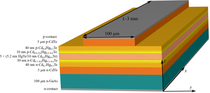
We consider a multiple quantum well laser structure grown on a (013)-oriented -GaAs substrate and consisting of an active region (five 5.2 nm HgTe QWs interleaved with 10 nm Cd0.6Hg0.4Te barriers), 70 nm CdxHg1-xTe waveguide layers ( varies between 0.6 and 0.7), and 5 m CdTe cladding layers (Fig. 1, Table 1).
This structure was simulated using a distributed drift-diffusion model based on one-dimensional (1D) Poisson’s equation and continuity equations for electrons and holes with taking into account the carrier capture and escape processes Afonenko and Ushakov (2014). Both radiative and Auger recombination were included in the model.
The bandstructure parameters were obtained from the eight-band method Novik et al. (2005); Aleshkin and Dubinov (2016). Quantum well depths for electrons and holes were calculated according to Refs. 30; 32. Carrier mobilities were interpolated from the experimental data of Ref. [Scott, 1972]. The calculated parameters of each heterostructure layer are collected in Table 1.
Internal optical losses and refractive index were calculated within the multioscillator Lorentz-Drude model including both phonon and free-carrier contributions Mroczkowski and Nelson (1983); Laurenti et al. (1990); Grynberg et al. (1974).
Distribution of the photon density across the resonator was found from the Bouguer–Lambert–Beer law.
Heating effects were taken into account by solving the 1D heat equation in the direction perpendicular to the heterostructure layers (we consider pulsed operation, when in-layer heat transfer during a pulse is negligible). We also included the temperature dependence of the bandgap in our model.
III Results and discussion
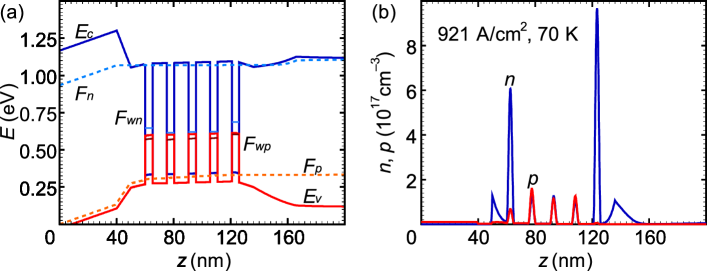
An example of calculated band diagrams and carrier distributions are shown in Fig. 2. The quasi-Fermi level difference inside the QWs is much smaller than in the barriers, meaning most of the carrier energy is dissipated into heat upon carrier capture into the QWs. One could try to increase the laser efficiency by lowering the barrier height; however, this is undesirable because it would boost Auger recombination in the barriers Aleshkin et al. (2019).
Another important observation is that the population inversion is distributed nonuniformly across the active region. To obtain larger gain, it is advantageous to use several quantum wells instead of a single one. Due to the low mobility of holes, the level of excitation of quantum wells decreases with distance from the -emitter. According to our calculations, is the optimal number of QWs, beyond which no significant increase in modal gain can be achieved.
Nonuniform carrier distribution can also appear in waveguide layers. We found that in constant-composition waveguides, small density and mobility of holes lead to carrier accumulation near the -cladding, with carrier density exceeding the nominal doping level by more than an order of magnitude. Putting a thin graded-composition CdxHg1-xTe layer near the -cladding with varying linearly between 0.8 and 0.6 eliminates carrier accumulation (Fig. 2b), which explains why experimentally measured lasing thresholds in structures with graded-composition layers were lower than in those with constant-composition layers Bleuse et al. (1999).
Bandgap difference between the adjacent waveguide layers (CdxHg1-xTe with and the barriers () results in good current confinement and negligible carrier leakage into the waveguide (electron quasi-Fermi level in the -doped waveguide layer and hole quasi-Fermi level in the -doped waveguide layer lie deep within the bandgap, Fig. 2 a).
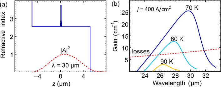
Figure 3a shows the good optical confinement of the TE0 mode provided by the heavily doped GaAs substrate (with nearly zero real part of the refractive index, see Fig. 3a) on one side of the heterostructure and a metal contact on the other side. The calculated total optical confinement factor of 5 QWs is . The reflection coefficients of the facets for the TE0 mode were estimated using eigenmode decomposition Ikegami (1972) as , at 30 m, which is much higher than the Fresnel reflection coefficient for a plane wave (0.2).
The good current and optical confinement result in modal gain exceeding the total optical loss (estimated as 7–12 cm-1 in the simulated structure) up to K (Fig. 3b), thus allowing laser operation slightly above the boiling point of liquid nitrogen. The gain maximum is shifted to shorter wavelengths with increasing temperature due to the temperature dependence of the bandgap.
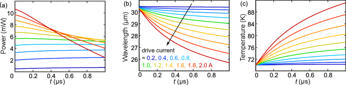
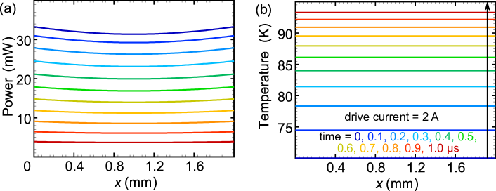
When discussing the operating temperature, one should take into account that the temperature of the active region can exceed the heat sink temperature, especially at large drive currents. In FIR lasers, heating issues are aggravated by the tight restrictions on the cladding doping level to avoid prohibitive optical losses. In our simulations, we used a doping level of cm-3 for the -cladding, resulting in resistance as high as 15 for a 2 mm-long and 100 m-wide resonator. Fig. 4 shows that, for a drive current of 2.0 A, the temperature of active region grows by 23 K during a 1 s pulse, the output power reduces from 10.6 to 2.4 mW, and the lasing wavelength shifts from 30.2 to 25.7 m.
On the other hand, good spatial uniformity of lasing and heating is maintained throughout the pulse. Fig. 5 shows that the lasing power and temperature are almost uniform across the resonator for reflection coefficients of the facets . However, if anti-reflective and highly reflective coatings are used, spatial nonuniformity may become pronounced, with the lasing power at the front facet being considerably higher than at the back facet.
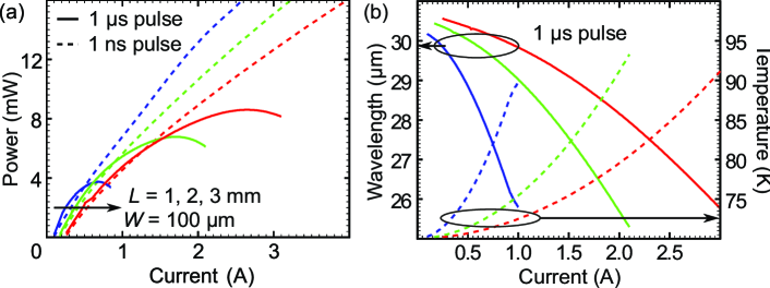
Finally, we calculated the output power of the laser under study. Figure 6 shows the output power, the temperature of the active region, and the lasing wavelength vs the drive current at three values of the resonator length: , 2, 3 mm. The resonator width is m. Maximum output power increases with the cavity length which results from weaker heating in longer cavity devices. At 1 s pulse length (quasi-CW mode), the maximum output power is 8.6 mW for mm. During the action of the pump pulse, the active region is heated and the radiation wavelength changes. As can be seen from the figure, the pulse-induced change in the wavelength and temperature are 4 m and 20 K, respectively (see Fig. 6b). Heating issues can be mitigated with shorter pulses, which allow to achieve several tens of mW output power (see Fig. 6a). It should be noted that a higher power in the initial part of the watt-ampere characteristics is realised at longer pump pulses. This is due to the heating of the active region during the pulse and a decrease in the laser wavelength, which leads to a decrease in internal losses (see Fig. 4).
IV Conclusions
We have theoretically demonstrated the feasibility of lasing under electrical pumping of HgTe quantum wells in the m wavelength range. This range of wavelengths lies in the phonon absorption (reststrahlen) band of GaAs-based compounds and is thus unattainable for existing quantum cascade lasers. The model used takes into account all necessary aspects of laser action, including drift and diffusion of carriers in the barrier layers, electron and hole capture of quantum wells, radiative and non-radiative Auger recombination, as well as heating of active region. According to the results of simulations, the laser action is possible at temperatures up to 90 K. At 70 K heat sink temperature, the average output power during a 1 s pulse can reach 9 mW. Feasibility of lasing at such long wavelengths and liquid nitrogen temperature is due to suppression of Auger recombination in narrow HgTe quantum wells which, in turn, is inherited from symmetric quasi-relativistic electron-hole dispersion.
Acknowledgements.
The work of DS and GA was supported by Russian Foundation for Basic Research, grant # 19-37-70031. AD, SM, and VG acknowledge the support of Russian Science Foundation, grant # 17-12-01360.Appendix A Distributed drift-diffusion model
To calculate the band diagrams, we used a model based on 1D Poisson’s equation and continuity equations for electrons and holes with taking into account nonuniform distribution of population inversion across the heterostructure Afonenko and Ushakov (2014). The main quantities in our distributed model are the electric potential and the electron and hole quasi-Fermi levels , , all of which depend on the coordinate along the growth direction. These quantities are found by numerically integrating Poisson’s equation together with the continuity equations for the electron and hole current densities , :
| (1) | ||||
Here, is the elementary charge, () is the electron (hole) density, () is the density of ionized acceptors (donors), is the relative permittivity of CdHgTe, is the vacuum permittivity, is the interband (nonradiative and spontaneous) recombination rate, is the modal gain, is the 3D photon density, is the group velocity of the lasing mode, and () is the electron (hole) mobility.
The total electron and hole densities , consist of the densities of delocalized carriers, contributing to the electric current:
| (2) | ||||
and densities of carriers localized in the quantum wells:
| (3) | ||||
Here, , (, ) are the 3D (2D) effective densities of states for electrons and holes, is the Boltzmann constant, and is the temperature. Logarithms and complete Fermi-Dirac integrals of order , , stem from integrating Fermi-Dirac distributions with quasi-Fermi levels , (for delocalized carriers) and (for localized carriers). Carrier states at th subband in a quantum well are described by wavefunctions , assuming the well spans the region . Subband edges , and effective densities of states were found from the eight-band method Novik et al. (2005); Aleshkin and Dubinov (2016).
3D photon density inside the -th well is connected to the 2D photon density by the optical confinement factor :
| (4) |
The dynamics of the localised carriers and 2D photon density was described by standard rate equations Afonenko and Ushakov (2014):
| (5) | ||||
where () is the 2D density of electrons (holes) localized in the th well, () is the density of delocalized carriers in the th well, () is the quasi-Fermi level difference between delocalized and localized electrons (holes), () is the characteristic time of electron (hole) capture into the well, is the contribution of the -th well to the modal gain, is the total loss, and are the total interband and spontaneous recombination rates, and is the fraction of spontaneous emission going into the lasing mode.
The total loss is the sum of external and internal contributions , , where can be further divided into the lattice absorption coefficient and the free-carrier absorption coefficient . The latter was assumed to be proportional to the carrier densities Mroczkowski and Nelson (1983); Li et al. (1996):
| (6) |
where and are the corresponding absorption cross sections.
Absorption cross sections calculated for CdTe within the Drude model at 30 m and 70 K are cm2 and cm2, in accordance with Refs. 34; 27. They set an upper limit to the CdTe waveguide doping at cm-3 Ushakov et al. (2020).
Spontaneous recombination rates and modal gain were calculated by considering direct optical transitions. Nonlinear effects were taken into account by the nonlinear gain parameter :
| (7) |
Appendix B Distributed model of the resonator and active region heating
To find the distribution of photon density across the resonator, we used the Bouguer–Lambert–Beer law for the photon densities , in two counterpropagating waves taking into account reflections at the facets Afonenko et al. (2018):
| (8) | ||||
where the -axis points in the direction of propagation of the first wave.
Modal gain and free-carrier absorption coefficient depend on the carrier densities, which can be found from the drift-diffusion model described in Appendix A. Equations (8) require dependencies and on the photon density . Instead of solving drift-diffusion equations (1) with given photon density we artificially change the lattice absorption coefficient to obtain the given photon density and the corresponding distribution of carrier densities. This allows us to obtain the functional dependences , by calculating , , and within the drift-diffusion model. Actually, the functions , were approximated by a bi-quadratic interpolation between 9 values calculated at a given current density and different , .
The evolution of local temperature inside the active region after the start of a pulse was found by using Green’s functions of the heat equation. Joule heating in the waveguide (including the active region) and in the cladding layers/substrate were considered separately, with corresponding Green’s functions , Afonenko et al. (2018):
| (9) | ||||
The heat power produced in the waveguide per unit area is given by Joule’s law minus the power transferred to the laser radiation:
| (10) | ||||
where is the current through the waveguide, is the associated voltage drop, is the modal gain, is the internal loss, is the 2D photon density in the lasing mode, and is the photon energy. The lasing frequency is time-dependent because heating affects the bandgap.
Green’s functions , were found by numerical solution of the one-dimensional heat equation along the -axis (perpendicular to the heterostructure layers) taking into account all epitaxial layers, the substrate, the solder, and the heat sink. Heat transfer along the -axis (parallel to the layers) was neglected. This approach is justified because the thermal diffusion length during the drive current pulse is much larger than the waveguide thickness, but much smaller than the substrate thickness, heat sink thickness, and resonator length. Assuming the pulse duration is s, the thermal diffusion length is m ( is the heat transfer coefficient Slack (1972)), while the active and emitter region thickness is m (Fig. 2).
Appendix C Calculation of Auger coefficients
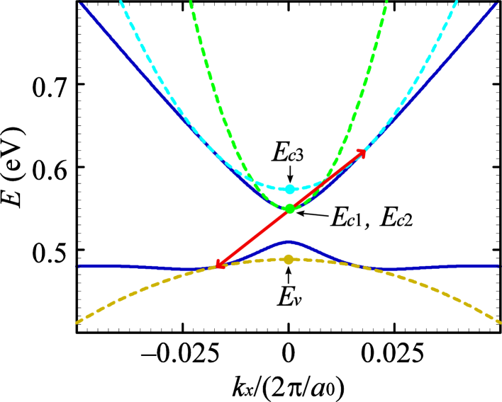
In the interband recombination rate we included both radiative and Auger recombination. In narrow-gap CdHgTe quantum wells the Auger recombination rate is dominated by the CCCH process Alymov et al. (2020). The strong nonparabolicity of the band dispersion complicates analytical treatment of Auger recombination, so we used parabolic interpolation near the states giving the dominant contribution to the Auger recombination rate (Fig. 7). In this approximation, two-dimensional Auger coefficient in a deep quantum well reads
| (11) | ||||
Here, and are the density-of-states effective masses of electrons and holes, , , , are the effective masses of the parabolic bands approximating the exact band dispersion, , , , are the edges of the parabolic bands, is the reduced Planck’s constant, and is the overlap integral.
Finite extension of carrier wavefunctions in direction is taken into account by the factor , which can be calculated for sinusoidal envelope wave functions as
| (12) |
where is the quantum well width, and
| (13) |
is the momentum transfer during the threshold Auger process (i. e., the process giving the dominant contribution to the Auger recombination rate). The calculated matrix element of the Bloch wave function overlap was 0.3, which agrees with the results of Lopes et al. (1993). Factor was 0.4, which is less than 0.6 calculated by formula (12), since the envelope wave function for electrons differs from the sinusoidal shape. For 5.2 nm-thick HgTe/Cd0.6Hg0.4Te quantum wells used in our simulations, the calculated Auger coefficient is cm4/s at 70 K and cm4/s at 90 K. The corresponding Auger coefficient defined in terms of 3D carrier densities is cm6/s at 70 K and cm6/s at 90 K. (The factor of appears when is averaged over the QW width assuming carrier wavefunctions are .)
References
- Neumaier et al. (2015) P. F.-X. Neumaier, K. Schmalz, J. Borngräber, R. Wylde, and H.-W. Hübers, “Terahertz gas-phase spectroscopy: chemometrics for security and medical applications,” Analyst 140, 213–222 (2015).
- Hochrein (2015) Thomas Hochrein, “Markets, availability, notice, and technical performance of terahertz systems: Historic development, present, and trends,” Journal of Infrared, Millimeter, and Terahertz Waves 36, 235 (2015).
- Dhillon et al. (2017) S S Dhillon, M S Vitiello, E H Linfield, A G Davies, Matthias C Hoffmann, John Booske, Claudio Paoloni, M Gensch, P Weightman, G P Williams, E Castro-Camus, D R S Cumming, F Simoens, I Escorcia-Carranza, J Grant, Stepan Lucyszyn, Makoto Kuwata-Gonokami, Kuniaki Konishi, Martin Koch, Charles A Schmuttenmaer, Tyler L Cocker, Rupert Huber, A G Markelz, Z D Taylor, Vincent P Wallace, J Axel Zeitler, Juraj Sibik, Timothy M Korter, B Ellison, S Rea, P Goldsmith, Ken B Cooper, Roger Appleby, D Pardo, P G Huggard, V Krozer, Haymen Shams, Martyn Fice, Cyril Renaud, Alwyn Seeds, Andreas Stöhr, Mira Naftaly, Nick Ridler, Roland Clarke, John E Cunningham, and Michael B Johnston, “The 2017 terahertz science and technology roadmap,” Journal of Physics D: Applied Physics 50, 043001 (2017).
- Vitiello et al. (2015) Miriam Serena Vitiello, Giacomo Scalari, Benjamin Williams, and Paolo De Natale, “Quantum cascade lasers: 20 years of challenges,” Opt. Express 23, 5167–5182 (2015).
- Ohtani et al. (2014) K. Ohtani, M. Beck, and J. Faist, “Double metal waveguide InGaAs/AlInAs quantum cascade lasers emitting at 24 m,” Applied Physics Letters 105, 121115 (2014).
- Loghmari et al. (2019) Z. Loghmari, M. Bahriz, A. Meguekam, R. Teissier, and A. N. Baranov, “InAs-based quantum cascade lasers emitting close to 25 m,” Electronics Letters 55, 144–146 (2019).
- Ohtani et al. (2016) Keita Ohtani, Mattias Beck, Martin Josef Süess, Jerome Faist, Aaron Maxwell Andrews, Tobias Zederbauer, Hermann Detz, Werner Schrenk, and Gottfried Strasser, “Far-infrared quantum cascade lasers operating in the AlAs phonon reststrahlen band,” ACS Photonics 3, 2280–2284 (2016).
- Rogalski (2005) A Rogalski, “HgCdTe infrared detector material: history, status and outlook,” Reports on Progress in Physics 68, 2267–2336 (2005).
- Bernevig et al. (2006) B. Andrei Bernevig, Taylor L. Hughes, and Shou-Cheng Zhang, “Quantum spin hall effect and topological phase transition in hgte quantum wells,” Science 314, 1757–1761 (2006).
- König et al. (2007) Markus König, Steffen Wiedmann, Christoph Brüne, Andreas Roth, Hartmut Buhmann, Laurens W. Molenkamp, Xiao-Liang Qi, and Shou-Cheng Zhang, “Quantum spin hall insulator state in hgte quantum wells,” Science 318, 766–770 (2007).
- Teppe et al. (2016) F. Teppe, M. Marcinkiewicz, S.S. Krishtopenko, S. Ruffenach, C. Consejo, A. M. Kadykov, W. Desrat, D. But, W. Knap, J. Ludwig, S. Moon, D. Smirnov, M. Orlita, Z. Jiang, S.V. Morozov, V.I. Gavrilenko, N.N. Mikhailov, and S.A. Dvoretskii, “Temperature-driven massless Kane fermions in HgCdTe crystals,” Nature Communications 7, 12576 (2016).
- Kadykov et al. (2018) A. M. Kadykov, S. S. Krishtopenko, B. Jouault, W. Desrat, W. Knap, S. Ruffenach, C. Consejo, J. Torres, S. V. Morozov, N. N. Mikhailov, S. A. Dvoretskii, and F. Teppe, “Temperature-induced topological phase transition in hgte quantum wells,” Phys. Rev. Lett. 120, 086401 (2018).
- Ruffenach et al. (2017) S. Ruffenach, A. Kadykov, V. V. Rumyantsev, J. Torres, D. Coquillat, D. But, S. S. Krishtopenko, C. Consejo, W. Knap, S. Winnerl, M. Helm, M. A. Fadeev, N. N. Mikhailov, S. A. Dvoretskii, V. I. Gavrilenko, S. V. Morozov, and F. Teppe, “HgCdTe-based heterostructures for terahertz photonics,” APL Materials 5, 035503 (2017).
- Maremyanin et al. (2018) K. V. Maremyanin, A. V. Ikonnikov, L. S. Bovkun, V. V. Rumyantsev, E. G. Chizhevskii, I. I. Zasavitskii, and V. I. Gavrilenko, “Terahertz injection lasers based on a PbSnSe solid solution with an emission wavelength up to 50 m and their application in the magnetospectroscopy of semiconductors,” Semiconductors 52, 1590–1594 (2018).
- Emtage (1976) P. R. Emtage, “Auger recombination and junction resistance in lead‐tin telluride,” Journal of Applied Physics 47, 2565–2568 (1976).
- Alymov et al. (2018) Georgy Alymov, Vladimir Vyurkov, Victor Ryzhii, Akira Satou, and Dmitry Svintsov, “Auger recombination in dirac materials: A tangle of many-body effects,” Phys. Rev. B 97, 205411 (2018).
- Abakumov et al. (1991) V. N. Abakumov, V. I. Perel, and I. N. Yassievich, Nonradiative Recombination in Semiconductors, Vol. 33 (Elsevier, 1991).
- Alymov et al. (2020) Georgy Alymov, Vladimir Rumyantsev, Sergey Morozov, Vladimir Gavrilenko, Vladimir Aleshkin, and Dmitry Svintsov, “Fundamental limits to far-infrared lasing in Auger-suppressed HgCdTe quantum wells,” ACS Photonics 7, 98–104 (2020).
- Morozov et al. (2016) S. V. Morozov, V. V. Rumyantsev, A. M. Kadykov, A. A. Dubinov, K. E. Kudryavtsev, A. V. Antonov, N. N. Mikhailov, S. A. Dvoretskii, and V. I. Gavrilenko, “Long wavelength stimulated emission up to 9.5 m from HgCdTe quantum well heterostructures,” Applied Physics Letters 108, 092104 (2016).
- Rumyantsev et al. (2018) VV Rumyantsev, NS Kulikov, AM Kadykov, MA Fadeev, AV Ikonnikov, AS Kazakov, MS Zholudev, V Ya Aleshkin, VV Utochkin, NN Mikhailov, et al., “Effect of features of the band spectrum on the characteristics of stimulated emission in narrow-gap heterostructures with hgcdte quantum wells,” Semiconductors 52, 1375–1379 (2018).
- Morozov et al. (2017) S. V. Morozov, V. V. Rumyantsev, M. A. Fadeev, M. S. Zholudev, K. E. Kudryavtsev, A. V. Antonov, A. M. Kadykov, A. A. Dubinov, N. N. Mikhailov, S. A. Dvoretsky, and V. I. Gavrilenko, “Stimulated emission from HgCdTe quantum well heterostructures at wavelengths up to 19.5 m,” Applied Physics Letters 111, 192101 (2017).
- Kudryavtsev et al. (2020) K. E. Kudryavtsev, V. V. Rumyantsev, V. Ya. Aleshkin, A. A. Dubinov, V. V. Utochkin, M. A. Fadeev, N. N. Mikhailov, G. Alymov, D. Svintsov, V. I. Gavrilenko, and S. V. Morozov, “Temperature limitations for stimulated emission in 3–4 m range due to threshold and non-threshold auger recombination in hgte/cdhgte quantum wells,” Applied Physics Letters 117, 083103 (2020).
- Melngailis and Strauss (1966) I. Melngailis and A. J. Strauss, “Spontaneous and coherent photoluminescence in CdxHg1-xTe,” Applied Physics Letters 8, 179–180 (1966).
- Arias et al. (1993) J M Arias, M Zandian, R Zucca, and J Singh, “HgCdTe infrared diode lasers grown by MBE,” Semiconductor Science and Technology 8, S255–S260 (1993).
- Bleuse et al. (1999) Joël Bleuse, Joël Bonnet-Gamard, Guido Mula, Noël Magnea, and Jean-Louis Pautrat, “Laser emission in HgCdTe in the 2–3.5 m range,” Journal of Crystal Growth 197, 529 – 536 (1999).
- Vurgaftman and Meyer (1998) I. Vurgaftman and J. R. Meyer, “High-temperature HgTe/CdTe multiple-quantum-well lasers,” Opt. Express 2, 137–142 (1998).
- Ushakov et al. (2020) Dmitrii Ushakov, Alexander Afonenko, Rustam Khabibullin, Dmitry Ponomarev, Vladimir Aleshkin, Sergey Morozov, and Alexander Dubinov, “HgCdTe-based quantum cascade lasers operating in the GaAs phonon Reststrahlen band predicted by the balance equation method,” Opt. Express 28, 25371–25382 (2020).
- Dubinov et al. (2019) A. A. Dubinov, V. Ya. Aleshkin, and S. V. Morozov, “Generation of THz radiation at a difference frequency in a HgCdTe-based laser,” Quantum Electronics 49, 689 (2019).
- Afonenko and Ushakov (2014) A.A. Afonenko and D.V. Ushakov, “Current-injection efficiency in semiconductor lasers with a waveguide based on quantum wells,” Semiconductors 48, 83–88 (2014).
- Novik et al. (2005) E. G. Novik, A. Pfeuffer-Jeschke, T. Jungwirth, V. Latussek, C. R. Becker, G. Landwehr, H. Buhmann, and L. W. Molenkamp, “Band structure of semimagnetic Hg1-yMnyTe quantum wells,” Phys. Rev. B 72, 035321 (2005).
- Aleshkin and Dubinov (2016) V.Ya. Aleshkin and A.A. Dubinov, “Effect of the spin–orbit interaction on intersubband electron transition in GaAs/AlGaAs quantum well heterostructures,” Physica B: Condensed Matter 503, 32 – 37 (2016).
- Van de Walle (1989) Chris G. Van de Walle, “Band lineups and deformation potentials in the model-solid theory,” Phys. Rev. B 39, 1871–1883 (1989).
- Scott (1972) Walter Scott, “Electron mobility in Hg1-xCdxTe,” Journal of Applied Physics 43, 1055–1062 (1972).
- Mroczkowski and Nelson (1983) J. A. Mroczkowski and D. A. Nelson, “Optical absorption below the absorption edge in Hg1-xCdxTe,” Journal of Applied Physics 54, 2041–2051 (1983).
- Laurenti et al. (1990) J. P. Laurenti, J. Camassel, A. Bouhemadou, B. Toulouse, R. Legros, and A. Lusson, “Temperature dependence of the fundamental absorption edge of mercury cadmium telluride,” Journal of Applied Physics 67, 6454–6460 (1990).
- Grynberg et al. (1974) M. Grynberg, R. Le Toullec, and M. Balkanski, “Dielectric function in HgTe between 8 and 300 K,” Phys. Rev. B 9, 517–526 (1974).
- Aleshkin et al. (2019) V Ya Aleshkin, A A Dubinov, V V Rumyantsev, and S V Morozov, “Threshold energies of Auger recombination in HgTe/CdHgTe quantum well heterostructures with 30–70 meV bandgap,” Journal of Physics: Condensed Matter 31, 425301 (2019).
- Ikegami (1972) T. Ikegami, “Reflectivity of mode at facet and oscillation mode in double-heterostructure injection lasers,” IEEE Journal of Quantum Electronics 8, 470–476 (1972).
- Li et al. (1996) Biao Li, J. H. Chu, Z. H. Chen, Y. Chang, H. M. Ji, and D. Y. Tang, “Free‐carrier absorption of Hg1-xCdxTe epitaxial films,” Journal of Applied Physics 79, 7738–7742 (1996).
- Afonenko et al. (2018) A.A. Afonenko, D.V. Ushakov, V.Ya. Aleshkin, A.A. Dubinov, N.V. Dikareva, S.M. Nekorkin, and B.N. Zvonkov, “Power characteristics of lasers with quantum-well waveguides and blocking layers,” Quantum Electronics 48, 390–394 (2018).
- Slack (1972) Glen A. Slack, “Thermal conductivity of II-VI compounds and phonon scattering by impurities,” Phys. Rev. B 6, 3791–3800 (1972).
- Lopes et al. (1993) V C Lopes, A J Syllaios, and M C Chen, “Minority carrier lifetime in mercury cadmium telluride,” Semiconductor Science and Technology 8, 824–841 (1993).