Materials design principles towards high hole mobility learning from an abnormally low hole mobility of silicon
Abstract
Si dominates the semiconductor industry material but possesses an abnormally low room temperature hole mobility (505 cm2/Vs), which is four times lower than that of Diamond and Ge ( cm2/Vs), two adjacent neighbors in the group IV column in the Periodic Table. In the past half-century, extensive efforts have been made to overcome the challenges of Si technology caused by low mobility in Si. However, the fundamental understanding of the underlying mechanisms remains lacking. Here, we theoretically reproduce the experimental data for conventional group IV and III-V semiconductors without involving adjustable parameters by curing the shortcoming of classical models. We uncover that the abnormally low hole mobility in Si originating from a combination of the strong interband scattering resulting from its weak spin-orbit coupling and the intensive participation of optical phonons in hole-phonon scattering. In contrast, the strong spin-orbit coupling in Ge leads to a negligible interband scattering; the strong bond and light atom mass in diamond give rise to high optical phonons frequency, preventing their participation in scattering. Based on these understandings rooted into the fundamental atomic properties, we present design principles for semiconducting materials towards high hole mobility.
Carrier mobility is one of the fundamental parameters of semiconductor materials since it governs the operation speed through the transit time across the device, the circuit operating frequency or the sensitivity in magnetic sensors sze_physics_2007 ; chuang_physics_2009 ; luque_lopez_handbook_2011 ; mahan_best_1996 ; novoselov_two-dimensional_2005 ; ishiwata_extremely_2013 . Increasing carrier mobility is one of the critical strategies to make microchips faster and more energy-efficient. Specifically, increasing carrier mobility can enhance the transistor drive current, which can, in turn, improve device performance or maintain performance and reduce power consumption pillarisetty_academic_2011 . Because the hole mobility ( cm2/Vs) is significantly lower than the electron mobility ( cm2/Vs) in Si pillarisetty_academic_2011 ; madelung_physics_1982 , the device performance of p-type transistor (PMOS) operates only at about one third the performance of n-type transistor (NMOS) goley_germanium_2014 . It stimulates tremendous efforts in past decades in seeking materials with high hole mobility to replace Si to substantially improve PMOS device performance to maximize microchip performance gains [7]. Comparing to Diamond and Ge, its two adjacent neighbors in group IV column of the Periodic Table that have more superior hole transport properties ( cm2/Vs and cm2/Vs respectively) noauthor_materials_nodate , the hole mobility in Si is unusually low with an abnormal trend adachi_properties_2005 . Although Si is the most well-documented semiconductor due to its dominance in the semiconductor industry, this abnormal trend in hole mobility is a long-standing puzzle. The underlying mechanisms remain ambiguous.
The lack of the fundamental understanding may due to the complexity of hole-phonon scattering in semiconductor valence bands kranzer_mobility_1974 , which contain essential complications, including the band degeneracy, the warping of the heavy-hole (hh) band, the p-type symmetry of the hole wave function, the influence of the light holes, and interband scattering between the light hole (lh) and hh bands kranzer_mobility_1974 ; wiley_lattice_1970 ; conwell_lattice_1959 ; bir_galvanomagnetic_1962 ; wiley_polar_1971 ; costato_hole_1972 . These complications require considerable modifications of the scattering models by incorporating many adjustable parameters such as deformation potentials for acoustic and optical phonons kranzer_mobility_1974 ; wiley_polar_1971 . It is arguable whether these adjustable parameters accurately contain all the effects of the complications mentioned above kranzer_mobility_1974 ; lawaetz_low-field_1968 , and a fortuitous agreement between the experimental values and simple model calculations may occur. For instance, experimentally measured hole mobility data can be fitted well both with and without polar-mode scattering for semiconductors wiley_lattice_1970 ; wiley_polar_1971 . In this sense, one usually ascribed the observed variation in hole mobility for group-IV and group-III-V materials to small variations in material parameters rather than different scattering mechanisms wiley_polar_1971 . A recently developed first-principles approach rooted in the Boltzmann transport equation seems to avoid such uncertainties giustino_electron-phonon_2017 ; ponce_towards_2018 ; ponce_hole_2019 . However, results show ponce_towards_2018 that the calculated hole mobilities for Si can vary by about 60% (from 502 to 820 cm2/Vs) depending on the levels of band structure theory used, illustrating the importance of accurate band structure to the carrier mobility. Furthermore, although first-principles calculations may own the advantage of treating transport problems in their full complexity, it is also desirable to gain more physical insights by examining the individual mechanisms affecting the hole transport properties.
In this work, we aim at elucidating the atomistic mechanisms underlying the abnormally low hole mobility in Si, rather than presenting an advanced method with improved accuracy. We calculate the phonon-limited hole mobilities of group IV and III-V semiconductors without adjustable parameters by employing the semi-empirical hole-phonon scattering theory kranzer_mobility_1974 ; yu_fundamentals_2010 in conjunction with experimental valence band parameters vurgaftman_band_2001 ; madelung_physics_1982 , and tight-binding approximations harrison_elementary_1999 to directly compute the adjustable parameters. The success of reproducing experimental data enables us to disentangle the contributions from various scattering mechanisms since the used method offers the advantage of providing physical insight into the problem at hand. We illustrate that, in comparison with Ge, the spin-orbit coupling (SOC) is so weak that hh-lh band splitting is tiny, causing strong interband hole-phonon scattering and the abnormal low hole mobility in Si. On the other hand, Diamond is even lighter but has a much stronger bond than Si, so it has a very high optical phonon frequency, which prevents it from participating in the hole scattering. It renders Diamond having high hole mobility. These new level understandings of the atomic mechanisms governing the hole mobility enable us to propose design principles to identify semiconducting materials with high hole mobility.
The carrier mobility is related to the average scattering time and conductivity effective mass: yu_fundamentals_2010 . In pure materials, is limited mainly by scattering of carriers by various types of phonons (lattice vibrations) kranzer_mobility_1974 ; yu_fundamentals_2010 ; seeger_semiconductor_2010 . Specifically, carriers can interact with phonons via deformation potentials since the band edge’s energy variation is related to the lattice strain caused by atomic displacement due to acoustic phonons shockley_energy_1950 and nonpolar optical phonons herring_transport_1956 . The former is called acoustic (AC) deformation potential scattering, and the latter is nonpolar optical (NPO) deformation potential scattering. In polar semiconductors, carriers can also couple with optical phonons via the induced longitudinal electrical field frohlich_electrons_1954 due to the macroscopic polarization field generated by the out-of-phase vibration [longitudinal-optical (LO) phonon] in electric dipoles tends to strongly couple with carriers, termed polar optical phonon (PO) scattering. An analogy of PO scattering to longitudinal-acoustic (LA) phonons is the piezoelectric scattering meijer_note_1953 . Here, we adopt semi-empirical scattering modes kranzer_mobility_1974 ; willardson_transport_1975 developed in the past forty years to calculate the hole mobility limited by these four hole-phonon scattering mechanisms, respectively. We then obtain the total hole mobility according to Matthiessen’s Rule hamaguchi_basic_2017 . Note that there are many band structure parameters involved in the semi-empirical scattering modes. Here, we use the Modified Beckea-Johnson (MBJ) potential becke_simple_2006 ; tran_accurate_2009 implemented in the Vienna ab-initio simulation package (VASP) kresse_efficiency_1996 to compute spin-orbit splitting energy for semiconductors under investigations. According to the tight-bonding model harrison_elementary_1999 , we get reasonable deformation potentials wiley_valence-band_1970 ; blacha_deformation_1984 ; harrison_electronic_1989 , phonon energy, elastic constants harrison_electronic_1989 ; baranowski_bond_1984 and dielectric constants samara_temperature_1983 ; burstein_c1_1965 to avoid the utilization of adjustable parameters as usual. The conductivity and density-of-states effective masses are obtained based on Luttinger parameters , , suggested commonly for III-V materials vurgaftman_band_2001 and group IV madelung_physics_1982 .We also consider the temperature-dependence of density-of-states conductivity effective mass linares_mobility_1979 ; barber_effective_1967 . Calculations are detailed in Supplemental Material, and related parameters are listed in Table S1-6.
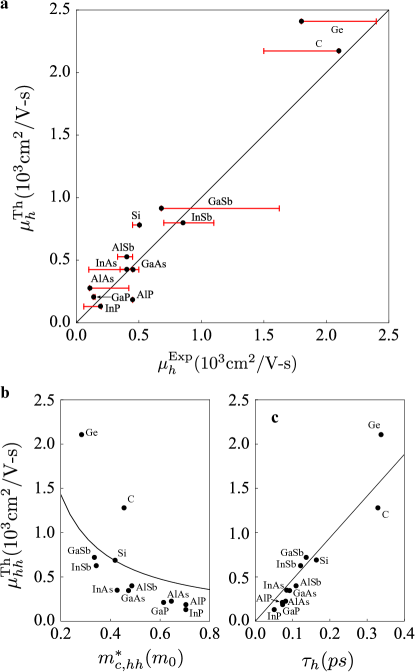
Fig. 1(a) shows our calculated room-temperature hole mobilities against corresponding experimental data madelung_physics_1982 ; noauthor_materials_nodate ; adachi_properties_2005 ; noauthor_nsm_nodate for group IV (Diamond, Si, and Ge) and group III-V (AlP, AlAs, AlSb, GaP, GaAs, GaSb, InP, InAs, and InSb) semiconductors. We use a range (marked by a red thick line) and single dot, respectively, to indicate multiple experimental values madelung_physics_1982 ; noauthor_materials_nodate ; adachi_properties_2005 ; noauthor_nsm_nodate and the value cited in the standard semiconductor handbook madelung_physics_1982 for each material. We find that the calculated values fall within the experimental range with a small scatter even though we adopted the semi-empirical hole-phonon scattering models. Specifically, the predicted Si hole mobility is 780 cm2/Vs against the suggested value of 505 cm2/Vs madelung_physics_1982 . If we change the set of Luttinger parameters to that suggested by Ref. ramos_structural_2001 , the predicted value becomes 580 cm2/Vs in a be better agreement with experimental value. However, the first-principles predicted data of Si hole mobility ranges widely from 502 to 820 cm2/Vs, depending on the functionals used in electronic band structure calculations ponce_towards_2018 , Thus, our prediction exhibits reasonable accuracy. The reliability of the simple isotropic relaxation time model used here has already been confirmed by Fischetti and Laux fischetti_band_1996 . They showed that the error introduced by neglecting the valence bands’ warping is less than 3% for Si (which has high anisotropy) and is negligible for Ge.
The extraordinary electron mobility of narrow band-gap semiconductors comes by virtue of their low effective mass ishiwata_extremely_2013 with the smallest band-gap InSb (0.17 eV at 300 K) possessing the highest ambient-temperature electron mobility (78,000 cm2/Vs) of all known conventional semiconductors durkop_extraordinary_2004 . However, the corresponding hole mobility in III-V semiconductors is orders of magnitude lower due to their considerably larger valence-band effective mass, together with their much shorter scattering time for hole transport than for electron transport pillarisetty_academic_2011 . To assess the relative significance of effective mass and scattering rate in limiting the hole mobility, we have to separate the contributions of holes from hh, lh, and split-off (so) bands. Fig.S2 and Fig.S3 (Supplemental Material) shows that the hole mobility is enhanced only slightly by the admixture of lh holes due to its much higher mobility. In the rest of this work, we will focus on holes in the hh band.
Fig. 1(b) shows the mobility against the hh conductivity mass for all considered semiconductors. We see that Ge and Diamond stand out clearly from remaining materials including Si. Specifically, Diamond has a similar effective mass as Si but is 2.5 times higher in (hh) hole mobility, demonstrating the hole-phonon scattering’s primer role in hole mobility. All semiconductors except Ge and Diamond follow a clear overall trend that a lower hole effective mass possesses higher hole mobility, consistent with the common perception. Such an overall trend is also evidenced by the model mobility (solid line in Fig. 1(b)) with an assumption of a constant hole scattering time (same as Si) but varying hole effective mass alone for all materials. It is expected for Ge and Diamond to have the superior hole mobility regarding non-polar group IV materials free from the polar scattering via optical phonons, which is a leading factor limiting the electron mobilities of group III-V semiconductors kranzer_mobility_1974 ; yu_fundamentals_2010 ; boer_semiconductor_2018 . However, it is difficult to understand why non-polar Si shares the same trend as the polar group III-V semiconductors.
An unrecognized, much stronger hole-phonon scattering causes this difficulty in Si relative to Diamond and Ge. We inspect the hole mobility against the scattering time for all considered semiconductors in Fig. 1(c). It exhibits an excellent linear relationship between hole mobility and relaxation time for all considered semiconductors irrespective of their remarkable difference in hole effective masses. Such a linear relationship implies the hole-phonon scattering taking the role over the effective mass in determining the hole mobility. Fig. 1(c) shows that Diamond and Ge have much longer scattering times than Si and all III-V materials. The short hole scattering time in group III-V semiconductors may arise from the polar scattering. However, as a non-polar semiconductor, Si possesses also a short hole scattering time, which is almost equal to that of polar semiconductors GaSb and InSb. Such short hole scattering time leads the hole mobility of Si to be only one-fourth of the hole mobilities of Ge and Diamond. The hole mobility of polar GaSb and InSb is even higher than that of non-polar Si due to their lighter hole effective masses. These exceptions imply complex hole-phonon scattering mechanisms in limiting the hole mobility in semiconductors. It is convenient to access the influence of each hole-phonon scattering mechanism ( = AC, NPO, PO, Pizo) on hole mobility since we deal with four scattering mechanisms separately. In non-polar group IV materials, the hole-phonon interactions are entirely governed by the deformation-potential scatterings due to both acoustic and optical phonons (particularly by longitudinal acoustic phonons (LA)). At room temperature, the valence band states occupied by holes are usually within meV of the valence band maximum (VBM), which is at the point, so their wavenumbers tend to be pretty small. In this sense, the most critical phonons are those of small wavenumber or long wavelengths. For each scattering mechanism , we can also separate interband and intraband scattering rates. Subsequently, we could decompose the total scattering time into various scattering mechanisms according to Matthiessen’s rule hamaguchi_basic_2017 ,
| (1) |
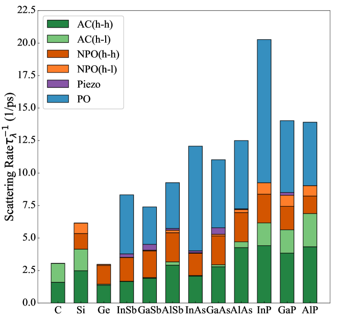
Fig. 2 displays the hole-phonon scattering rate of each scattering channel for all considered semiconductors. As expected, the piezoelectric scattering is absent in group IV semiconductors and is negligibly small relative to other scattering mechanisms yu_fundamentals_2010 in all group III-V semiconductors. The sizeable polar scattering indeed yields polar group III-V semiconductors with much shorter total scattering time than non-polar group IV semiconductors, except Si. Among group III-V semiconductors, a significant variation occurs in the polar scattering rates: it plays a primary role in InAs, InSb, and InP (67%, 55%, and 54%, respectively), but a minor role in GaSb and AlSb (less than 38%). We find that the interband scattering channel substantially enhances the hole-phonon scattering in Diamond, Si, InP, GaP, and AlP. In Ge, however, such interband scattering is suppressed, rendering Ge has an almost three times longer scattering time than Si. From the comparison between Si and GaSb and InSb, we also see that the suppression of the interband scattering compensates the finite PO scattering in GaSb and InSb, yielding the total scattering times in GaSb and InSb almost the same as in Si. The reason makes Diamond having a three times longer scattering time than Si is, however, completely different since the Diamond benefits from the vanishing of NPO scattering and reduction in AC scattering rate. The different reasons resulting in the super hole mobilities in Diamond and Ge imply compelling physics limiting the hole mobility in semiconductors.
The hole-phonon interband scattering is strongly related to the SOC strength in semiconductors. In common semiconductors, the VBM is located at point where hh and lh bands are degenerate and above the spin-orbit split-off (SO) band by an energy separation of spin-orbit splitting . Away from the point, the degeneracy of hh and lh bands is lifted by SOC with corresponding hh-lh splitting, which is proportional to harrison_elementary_1999 , along the and directions shown in Fig. 3(d) for Diamond, Si, and Ge. It is straightforward to learn that the hh-lh splitting determines the number of phonons required to supply the required energy for scattering holes from hh band to lh band resulting from the energy conservation phonon scattering processes. The interband scattering rate is thus exponentially dependent on the inverse of hh-lh splitting. Subsequently, in semiconductors with a strong SOC, the interband scattering occurs only within an extremely small k range nearby the point, which means only a tiny part of holes having the opportunity to involve in the interband scattering. In striking contrast, in semiconductors with a weak SOC, most holes have the opportunity to participate in the interband scattering. Thus, Diamond, Si, InP, GaP, and AlP constituted by light (anion) atom have much stronger interband scattering owing to their small SOC than the remaining semiconductors. Such interband scattering was regarded as very ineffective in group III-V semiconductors wiley_polar_1971 , and thus intraband scatterings are usually considered thoroughly to reproduce experimental data by adjusting the deformation potentials. Here, we demonstrate its critical role explicitly to address the abnormal low hole mobility in Si relative to Ge.
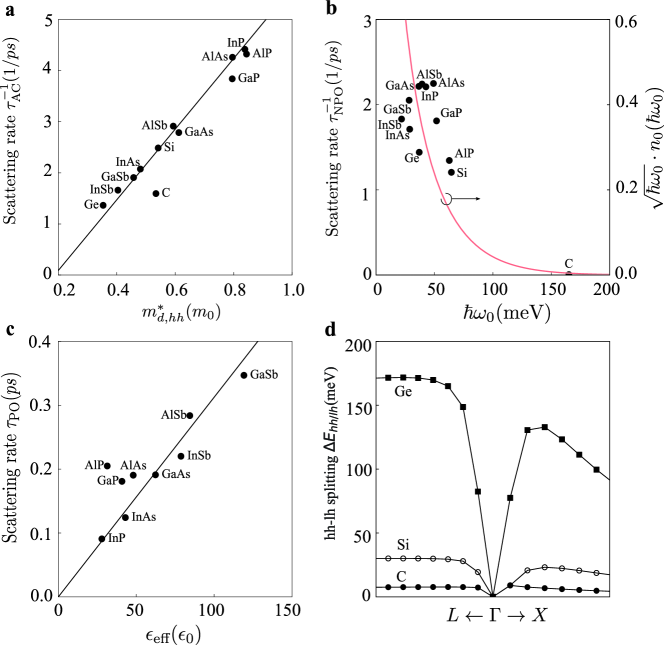
The intraband AC scattering rate depends mainly on the effective DOS mass of hh band subjected to stronger phonon scatterings arising from a larger density of final states: . Fig. 3(a) exhibits an excellent linear relationship between and for all considered semiconductors except Diamond. Super hard Diamond owns a huge average elastic constant , making AC phonons possess an exceptionally large group velocity since it is proportional to . The group velocity leads large-q AC phonons to have too high frequency to be unoccupied at room temperature. This giant group velocity prevents AC phonons from the interaction with holes in Diamond, making its below the overall trend of other materials, as shown in Fig. 3(a). It is also particularly interesting to understand why the ultrawide band-gap Diamond has an even smaller effective mass than Si. Suppose we neglect the warping of the valence bands for a moment. In this sense, we can evaluate by inspecting , where and are energy separation and energy equivalent to momentum matrix element Q between -like conduction band ( for ZB) and p-like valence band ( for ZB) at point, respectively. scales inversely with the square of the bond length d, giving rise to , 3.4, and 7.6 eV in Ge, Si, and Diamond. Whereas is usually found to be material-independent yu_fundamentals_2010 resulting from the complementation from occupied d electrons as pointed out by Lawaetz lawaetz_valence-band_1971 , who found that in the absence of d electrons scales inversely with the square of bond length. A 35% shorter bond length in Diamond makes its two times bigger than Si lawaetz_valence-band_1971 . In combination with a ratio of 0.45 in , it results Diamond and Si possessing similar despite their remarkable difference in band-gap. In the remaining materials, the variation in is not so large lawaetz_valence-band_1971 that is highly correlated with their . In polar semiconductors, depends mainly on the energy separation of cation orbital and anion orbital and is thus determined by their anion orbitals due to their cation orbitals (Al 3, Ga 4, and In 5) are almost the same. The energy position of anion orbitals is in descending order from Sb, to As, to P, to N. Specifically, N orbital is remarkable below remaining anion orbitals in energy (Fig.S4), giving rise to a much larger in III-nitrides. Thus, we expect III-nitrides to be very heavy in hh band’s effective mass, which was recently found to be the leading factor causing their exceptionally poor hole mobilities ponce_route_2019 . From III-Sb through III-As to III-P, we deduce that the hh effective mass gets heavier and hence gets larger in with the only exceptions of AlSb and AlAs, as shown in Fig. 1(b). Such exceptions are due to their significant warping of hh band due to much higher Al orbital than remaining cation orbitals.
For a semiconductor, the optical phonon frequency governs mainly the NPO scattering since , where s the Bose-Einstein occupation of the optical phonon with energy . Fig. 3(b) shows against for all considered semiconductors, exhibiting a nice correlation between and as indicated by a curve of . We find that Diamond has a vanishing NPO scattering rate because it has an extremely large meV adachi_properties_2005 , making the optical phonons unoccupied at room temperature. Si also benefits from its sizeable meV to have a small intraband NPO scattering rate . Harrison harrison_elementary_1999 proposed for material MX, where ( and are masses of the two constituent atoms M and X). Materials are expected to have simultaneously an extremely small value in reduced mass and bond length if one of its constituent atoms is of utmost light (small). It prefers elements (Be, B, N, C, O, and F) in the second row of the periodic table. Therefore, Diamond, III-Nitride and Boron-V materials have large , preventing their optical phonons from participating the NPO scattering (as well as PO scattering in polar materials) in those materials.
To understand why polar material GaSb has a higher hole mobility than Si, it is crucial to reveal the atomic mechanism underlying the PO scattering in polar materials. To do so, we show in Fig. 3(c) the PO scattering rate against the effective dielectric constant ( is the static dielectric constant and the high-frequency optical dielectric constant) for group III-V semiconductors. It exhibits that the PO scattering rate is highly correlated with due to it screens the macroscopic polarization field induced by the LO phonons according to Howarth howarth_theory_1953 and Wiley wiley_polar_1971 (Fig.S6 and Fig.S7). Because InP and GaSb have the smallest and largest , their polar scattering is the strongest and weakest, respectively, among these group III-V semiconductors. Regarding the static dielectric constant of the solids is the sum of electronic and lattice contributions, ( is also the optical dielectric constant ), we can rewrite . A longer bond length enhances the electronic response to external electric field increases and screening effect on the external field. Thus, is generally proportional to the bond length (Fig.S5). Furthermore, scales with , where is the covalency defined by Harrison harrison_elementary_1999 . GaSb has the smallest - and - energy separations between cation and anion (Fig.S4) over considered group III-V semiconductors, which render it the strongest covalency and thus the smallest . In combination with a sizable bond length and large in GaSb, it causes GaSb to have the largest and the weakest polar scattering. Whereas InP holds the smallest - energy separation and one of the smallest - energy separations among group III-V semiconductors, rendering it to have the weakest covalency and largest , making InP the smallest and thus strongest polar scattering.
Design principles towards high hole mobility. We have learned that Si has abnormally low hole mobility because Si possesses a weak SOC resulting from the light atom and strong hole-phonon interband scattering. Compared with Ge, the weak SOC leads to small splitting in the valence bands away from ; therefore, it cannot suppress the interband scattering. Moreover, the short Si-Si bond enhances the coupling between orbitals to yield a larger - band-gap and, thus, a heavier hole mass than Ge. On the other hand, compared with Diamond, Si is not light (small) enough to remarkably raise the optical phonons’ frequency to prevent optical phonons from participating in the NPO scattering. Because the optical phonon frequency scales inversely with the square of bond length, we suggest choosing at least one of the constituent atoms from the second row in the Periodic Table (e.g., Be, B, N, C, and O) for semiconducting materials. It will own an extremely short bond length to raise the frequency of optical phonons to eliminate the NPO scattering and PO scattering (in polar materials). High-frequency optical phonons are insufficient to possess high hole mobility because the heavy hole mass and interband scattering will also deteriorate the hole mobility through the remaining AC scattering. For instance, the hole mobility of SiC (cm2/Vs) is not the average of Diamond and Si, but is a factor of 5 smaller than Si meng_phonon-limited_2019 . This surprising behavior arises from a much heavier hole mass than both Diamond and Si regarding . C 2 orbital is about 2 eV below the Si orbital, which renders SiC has a larger - band-gap but smaller - momentum matrix element than both Diamond and Si and yields a much heavier hole mass in SiC. Therefore, we should design materials to have VBM derived from a heavy anion with strong SOC to split the valence bands and a small p-p energy separation between anion and cation to have a light hole mass. From those design principles, we can exclude nitrides ponce_route_2019 and oxides madelung_physics_1982 (e.g., the reported hole mobility of ZnO is 0.5-3.5 cm2/Vs norton2004zno ) for high hole mobility considering much larger electronegativity of N and O than other elements, which will yield a sizable - band-gap and hence heavy hole mass in compounds. In a high-throughput computational screening, there are only very few oxides out of 3,052 oxides are predicted to have small hole mass hautier2013identification , which are tentatively ascribed to the hybridization between cation and O or between O and another anionic . The low hole mobility, which is typically lower than 5 cm2/Vs, is the main challenge impeding implementation of p-type transparent conducting oxides yu_metal_2016 . According to our understanding, boron-containing III-V materials liu_simultaneously_2018 are indeed expected to have high hole mobility and, more specifically, BAs should have higher hole mobility than BP due to its strong SOC. In addition to these second row elements, we should choose semiconducting materials made by cation and anion with small difference in atom size and orbital energy. The former gives rise to a longer bond length, and the latter gives rise to a light hole mass and a large effective dielectric constant, which will benefit the reduction of PO scattering.
Acknowledgements.
This work was supported by the National Science Foundation for Distinguished Young Scholars under Grant No. 11925407 and the Key Research Program of Frontier Sciences, CAS under Grant No. ZDBS-LY-JSC019. S.H.W. was supported by the NSFC under Grant No. 11634003, 11991060, and U1930402 and the National Key Research and Development Program of China under Grant No. 2016YFB0700700.References
- (1) Sze, S. M. & Ng, K. K. Physics of semiconductor devices (Wiley-Interscience, Hoboken, NJ, 2007), third edition edn. OCLC: 255534639.
- (2) Chuang, S. L. Physics of photonic devices. Wiley series in pure and applied optics (John Wiley & Sons, Hoboken, N.J, 2009), 2nd ed edn. OCLC: ocn228676792.
- (3) Luque López, A. & Hegedus, S. (eds.) Handbook of photovoltaic science and engineering (Wiley, Chichester, 2011), 2. ed., [fully rev. and updated] edn. OCLC: 845812578.
- (4) Mahan, G. D. & Sofo, J. O. The best thermoelectric. Proceedings of the National Academy of Sciences 93, 7436–7439 (1996).
- (5) Novoselov, K. S. et al. Two-dimensional gas of massless Dirac fermions in graphene. Nature 438, 197–200 (2005).
- (6) Ishiwata, S. et al. Extremely high electron mobility in a phonon-glass semimetal. Nature Materials 12, 512–517 (2013).
- (7) Pillarisetty, R. Academic and industry research progress in germanium nanodevices. Nature 479, 324–328 (2011).
- (8) Bimberg, D. et al. Physics of Group IV Elements and III-V Compounds / Physik der Elemente der IV. Gruppe und der III-V Verbindungen. Condensed Matter (Springer-Verlag, Berlin Heidelberg, 1982).
- (9) Goley, P. & Hudait, M. Germanium Based Field-Effect Transistors: Challenges and Opportunities. Materials 7, 2301–2339 (2014).
- (10) Materials Science Articles | Latest Science Articles | Scientific Development.
- (11) Adachi, S. Properties of Group-IV, III-V and II-VI Semiconductors: Adachi/Properties of Group-IV, III-V and II-VI Semiconductors (John Wiley & Sons, Ltd, Chichester, UK, 2005).
- (12) Kranzer, D. Mobility of holes of zinc-blende III–V and II–VI compounds. Physica Status Solidi (a) 26, 11–52 (1974).
- (13) Wiley, J. D. & DiDomenico, M. Lattice Mobility of Holes in III-V Compounds. Physical Review B 2, 427–433 (1970).
- (14) Conwell, E. Lattice mobility of hot carriers. Journal of Physics and Chemistry of Solids 8, 234–239 (1959).
- (15) Bir, G. I., Normantas, E. & Pikus, G. E. Galvanomagnetic effects in semiconductors with degenerate zones. Soviet Physics-Solid State 4, 867–877 (1962).
- (16) Wiley, J. D. Polar Mobility of Holes in III-V Compounds. Physical Review B 4, 2485–2493 (1971).
- (17) Costato, M., Jacoboni, C. & Reggiani, L. Hole Transport in Polar Semiconductors. Physica Status Solidi (b) 52, 461–473 (1972).
- (18) Lawaetz, P. Low-Field Mobility and Galvanomagnetic Properties of Holes in Germanium with Phonon Scattering. Physical Review 174, 867–880 (1968).
- (19) Giustino, F. Electron-phonon interactions from first principles. Reviews of Modern Physics 89, 015003 (2017).
- (20) Poncé, S., Margine, E. R. & Giustino, F. Towards predictive many-body calculations of phonon-limited carrier mobilities in semiconductors. Physical Review B 97, 121201 (2018).
- (21) Poncé, S., Jena, D. & Giustino, F. Hole mobility of strained GaN from first principles. Physical Review B 100, 085204 (2019).
- (22) Yu, P. Y. & Cardona, M. Fundamentals of semiconductors: physics and materials properties. Graduate texts in physics (Springer, Berlin, 2010), 4. ed edn. OCLC: 390878032.
- (23) Vurgaftman, I., Meyer, J. R. & Ram-Mohan, L. R. Band parameters for III–V compound semiconductors and their alloys. Journal of Applied Physics 89, 5815–5875 (2001).
- (24) Harrison, W. A. Elementary electronic structure (World Scientific, Singapore ; River Edge, NJ, 1999).
- (25) Seeger, K. Semiconductor Physics: an introduction. Advanced Texts in Physics (Springer Berlin, Berlin, 2010), 9. ed edn. OCLC: 846198919.
- (26) Shockley, W. & Bardeen, J. Energy Bands and Mobilities in Monatomic Semiconductors. Physical Review 77, 407–408 (1950).
- (27) Herring, C. & Vogt, E. Transport and Deformation-Potential Theory for Many-Valley Semiconductors with Anisotropic Scattering. Physical Review 101, 944–961 (1956).
- (28) Fröhlich, H. Electrons in lattice fields. Advances in Physics 3, 325–361 (1954).
- (29) Meijer, H. & Polder, D. Note on polar scattering of conduction electrons in regular crystals. Physica 19, 255–264 (1953).
- (30) Willardson, R. K. & Beer, A. C. Transport phenomena. No. 10 in Semiconductors and semimetals (Academic Press, New York, NY, 1975). OCLC: 123220025.
- (31) Hamaguchi, C. Basic semiconductor physics. Graduate texts in physics (Springer, Cham, 2017), third edition edn. OCLC: ocn994820645.
- (32) Becke, A. D. & Johnson, E. R. A simple effective potential for exchange. The Journal of Chemical Physics 124, 221101 (2006).
- (33) Tran, F. & Blaha, P. Accurate Band Gaps of Semiconductors and Insulators with a Semilocal Exchange-Correlation Potential. Physical Review Letters 102, 226401 (2009).
- (34) Kresse, G. & Furthmüller, J. Efficiency of ab-initio total energy calculations for metals and semiconductors using a plane-wave basis set. Computational Materials Science 6, 15–50 (1996).
- (35) Wiley, J. Valence-band deformation potentials for the III–V compounds. Solid State Communications 8, 1865–1868 (1970).
- (36) Blacha, A., Presting, H. & Cardona, M. Deformation Potentials of k = 0 States of Tetrahedral Semiconductors. physica status solidi (b) 126, 11–36 (1984).
- (37) Harrison, W. A. Electronic structure and the properties of solids: the physics of the chemical bond (Dover Publications, New York, 1989), dover ed edn.
- (38) Baranowski, J. M. Bond lengths, force constants and local impurity distortions in semiconductors. Journal of Physics C: Solid State Physics 17, 6287–6301 (1984).
- (39) Samara, G. A. Temperature and pressure dependences of the dielectric constants of semiconductors. Physical Review B 27, 3494–3505 (1983).
- (40) Burstein, E. C1 - THE INTRINSIC INFRARED AND RAMAN LATTICE VIBRATION SPECTRA OF CUBIC DIATOMIC CRYSTALS**Supported in part by the U.S. Atomic Energy Commission. In Wallis, R. F. (ed.) Lattice Dynamics, 315–336 (Pergamon, 1965).
- (41) Linares, L. C. The mobility, resistivity and carrier density in P-type silicon doped with boron, gallium and indium. Ph.D. thesis (1979). Journal Abbreviation: Ph.D. Thesis Publication Title: Ph.D. Thesis.
- (42) Barber, H. Effective mass and intrinsic concentration in silicon. Solid-State Electronics 10, 1039–1051 (1967).
- (43) NSM Archive - Physical Properties of Semiconductors. URL http://www.ioffe.ru/SVA/NSM/Semicond/.
- (44) Ramos, L. E. et al. Structural, electronic, and effective-mass properties of silicon and zinc-blende group-III nitride semiconductor compounds. Physical Review B 63, 165210 (2001).
- (45) Fischetti, M. V. & Laux, S. E. Band structure, deformation potentials, and carrier mobility in strained Si, Ge, and SiGe alloys. Journal of Applied Physics 80, 2234–2252 (1996).
- (46) Dürkop, T., Getty, S. A., Cobas, E. & Fuhrer, M. S. Extraordinary Mobility in Semiconducting Carbon Nanotubes. Nano Letters 4, 35–39 (2004).
- (47) Boer, K. W. Semiconductor physics (Springer Berlin Heidelberg, New York, NY, 2018).
- (48) Lawaetz, P. Valence-Band Parameters in Cubic Semiconductors. Physical Review B 4, 3460–3467 (1971).
- (49) Poncé, S., Jena, D. & Giustino, F. Route to High Hole Mobility in GaN via Reversal of Crystal-Field Splitting. Physical Review Letters 123, 096602 (2019).
- (50) Howarth, D. J. & Sondheimer, E. H. The Theory of Electronic Conduction in Polar Semi-Conductors. Proceedings of the Royal Society of London Series A 219, 53–74 (1953).
- (51) Meng, F., Ma, J., He, J. & Li, W. Phonon-limited carrier mobility and temperature-dependent scattering mechanism of 3C -SiC from first principles. Physical Review B 99, 045201 (2019).
- (52) Norton, D. P. et al. Zno: growth, doping processing. Materials Today 7, 34–40 (2004).
- (53) Hautier, G., Miglio, A., Ceder, G., Rignanese, G. & Gonze, X. Identification and design principles of low hole effective mass p-type transparent conducting oxides. Nature Communications 4, 2292–2292 (2013).
- (54) Yu, X., Marks, T. J. & Facchetti, A. Metal oxides for optoelectronic applications. Nature Materials 15, 383–396 (2016).
- (55) Liu, T.-H. et al. Simultaneously high electron and hole mobilities in cubic boron-V compounds: BP, BAs, and BSb. Physical Review B 98, 081203 (2018).