A Low-Loss 1-4 GHz Optically-Controlled Silicon Plasma Switch
Abstract
This paper presents a low-loss optically-controlled inline RF switch suitable for L- and S-band applications. Under 1.5 W laser power, the switch exhibits a measured ON-state insertion loss of less than 0.33 dB and return loss better than 20 dB across the band. The measured OFF-state isolation ranges from 27 dB at 1 GHz to 17 dB at 4 GHz. The switch comprises a single silicon chiplet excited by a 915-nm laser fiber which creates electron-hole pairs, thereby exciting the ON-state silicon plasma. An optical fiber is guided through the bottom of the RF substrate to illuminate the chiplet, which bridges a 1.075-mm microstrip line gap. To the best of our knowledge, this is the lowest-loss silicon plasma switch demonstrated today.
Keywords:
silicon plasma technology, fiber lasers, optical switch, optically-induced plasmas (OIP).I Introduction
Optically-tunable RF circuits offer a variety of attributes, such as fast switching speeds and tunability, without moving mechanical parts. Additionally, these switches provide high power handling at a low production cost when compared to conventional RF switching technologies.
Current literature discusses utilizing silicon plasma as switches for a variety of applications [1, 2, 3, 4, 5, 6, 7, 8, 9, 10, 11]. Researchers in [1, 2, 5] focus on the linearity, showing measured IIP3 as high as +77 dBm. Although the reported results primarily focus on switches and applications thereof (e.g. [7] and [9, 12] focus on antennas and matching networks respectively), [13, 14, 15] have used similar silicon plasma technology to realize variable attenuators.
This technology requires the inclusion of laser diodes to control the plasma state (ON or OFF) in the semiconductor chiplet. This biasing network is relatively straightforward, as it is naturally decoupled from the direct RF path. A relatively recent application domain of this technology is in 5G base stations since these systems require 1) high power handling, 2) fast switching speeds, 3) low cost, and 4) small footprint switching solutions [1], [5].
This work improves upon the current state of the art by demonstrating the lowest insertion loss switch in the L and S bands [2]. Additionally, it demonstrates this technology as an SMD replacement for current attenuators, due to the continuously varying response to incident laser power. Moreover, it investigates RF performance improvements achievable by extending power capabilities of the laser bias.
II Theory
When a high-energy photon impinges upon a semiconductor, an electron-hole pair is produced. The accepted bandgap of silicon is 1.12 eV at room temperature, meaning incident light with a wavelength shorter than about one micron can initiate such a phenomenon. However, empirical data in [13] shows that longer wavelengths, which still create an electron-hole pair, can provide greater penetration into the silicon.
The closed-form expression for exited carriers generated as a function of depth, z, into the sample is given originally by [4] and improved upon by [16] to account for higher radiant fluxes ( )
| (1) |
where is the quantum efficiency, is the absorption coefficient, is the majority carrier lifetime, is the power of the laser, is the incident laser light’s wavelength, is the incident area, is the reflection from the surface, is the diffusion length, and is the saturation velocity at the surface. Certain wavelengths around 800-1000 nm emperically have the best quantum efficiency, lending to a higher probability that all the photon packets will be absorbed and create electron-hole pairs. The reflection remains constant around 0.3 for all wavelengths in this range.
III Design
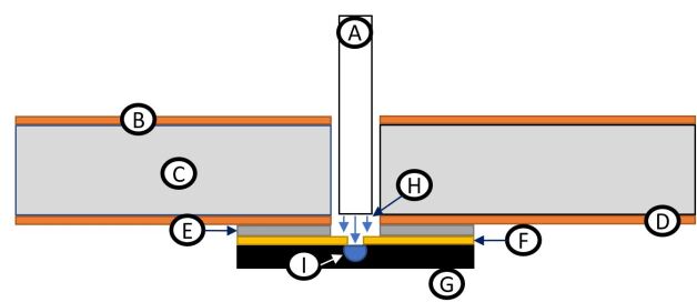
The design consists of a simple microstrip line with a small through gap that has been optimized for the 1 to 4 GHz frequency range. A silicon chiplet is assembled over a small gap in the microstrip line. The chiplet is plated with gold on one side with a small centered gap. This gap is crucial as it exposes the silicon such that laser illumination may be introduced by a fiber which is inserted from the bottom of the RF substrate. As a result, this induces the silicon plasma and creates conduction. A more detailed view may be seen in Fig. 1.
In order to optimize the ON/OFF ratio, a 200 m lightly doped n-type silicon wafer is selected to manufacture the chiplet. With a phosphorous doping concentration of about (3000 ), more free carriers are initially present, when compared to intrinsic silicon, allowing better insertion loss. This preserves a high degree of isolation, which increases the ON/OFF ratio of the switch. A 915-nm wavelength laser is used, as this provides both high quantum efficiency and deep penetration into the chiplet, allowing better contact with the gold. The laser output power varies continuously up to 1.5 W, ensuring that the achievable conductivity has a wide range.
The silicon chiplets are sputtered with 2 m of gold on one side and measure 3.075 mm by 500 m by 200 m (length by width by height) with a 75-m gap in the gold in the middle. This gap allows the 100 m fiber to illuminate the exposed silicon, permitting the two sides to conduct.
The chiplets are custom manufactured in-house. First, the 4-inch bare die is sputtered with titanium to form a coating 20 nm in thickness, allowing good adhesion to the semiconductor. Thereafter, a 2 m gold layer is sputtered on top. After lithography, the 75-m gap is etched of both gold and titanium. A dicing saw is then used to create the aforementioned sizes, which are comparable to current SMDs.
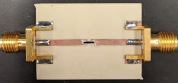
The RF board is a 30 mil TMM3 () substrate with 17.5 m of copper thickness. The top pattern is a simple 50- microstrip through with a 1.075 mm gap in the middle. A via is drilled in the center of this gap for the fiber. The final board is shown in Fig. 2.
The chiplet is assembled over and contacted to the microstrip line using silver epoxy. A 200 m non-plated via, directly under the 75 m exposed silicon, allows the fiber to be inserted through the RF substrate. The stack up depicted in Fig. 1 is comparable to [1, 2], except a micromanipulator (which can be seen in Fig. 3) is used to guide the fiber through the via. Furthermore, the chiplet is attached to the board much like an SMD, rather than compressed against the board and capacitavely coupled. This contributes to improved RF performance. Note that the RF board is technically upside-down during optical excitation to allow the micromanipulator to position the fiber through the via on the bottom side of the board. While testing, the board is raised from the table to reduce any effects from materials other than free space.
IV Measurements
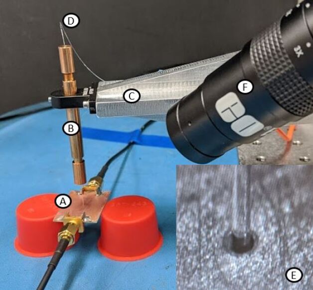
The set up consists of a 1.5-W, quasi-CW fiber-coupled laser from Sheaumann lasers centered at 915 nm. The multimode fiber has a nominal diameter of 100 m and is cleaved at the end to allow for free space coupling. The fiber is held by a fiber chuck which is affixed to a cantilevered arm, connected to a three-axis micromanipulator for precise positioning of the fiber’s tip. In the set up, shown in Fig. 3, a camera is focused on the location of the via, displaying the fiber’s position. Once the fiber is in the via, it is lowered until contact is made with the silicon chiplet, then raised by several microns. This allows the light to disperse which increases the contact area on the silicon, forming better contact between the two gold sides of the chiplet.
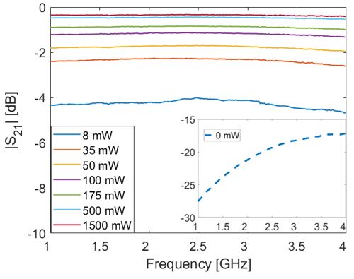
The board is excited under nominal RF power while varying the laser power. Constant closed-loop monitoring is used to control the diode’s junction temperature to be within 10∘ C of ambient. The laser power is varied from 0 mW up to 1.5 W.
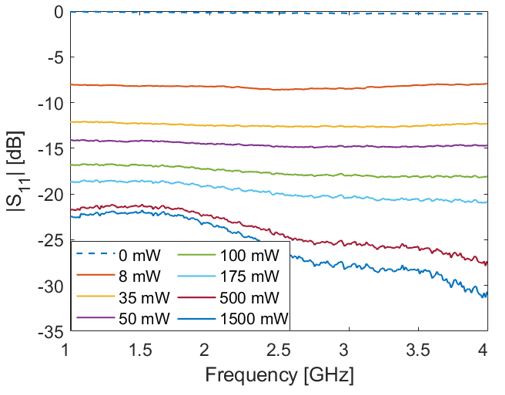
Measured results from the switch are shown in Figs. 4a and 4b. Under no laser illumination (i.e. 0 mW) the isolation is greater than 17 dB and the return loss is less than 0.30 dB for the 1 to 4 GHz range. Upon illumination, the chiplet approximates a short circuit. Note that this trend is continuously varying, allowing the chiplet to act as a variable attenuator controlled by the illumination power.
IV-A Comparison with State of the Art
Table 1 shows the current literature focused on creating silicon plasma switches. It is important to note that the advanced results achieved in this work are not solely attributed to increases in power, as results surpassing the state of the art are achieved at similar powers.
IV-B Circuit Model
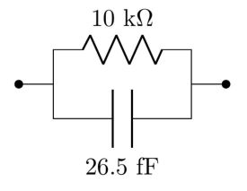
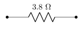
In Fig. 5a, a simplified equivalent circuit model for the switch’s OFF state is seen. The resistor, which dominates the performance at lower frequencies, is due to the bulk resistivity of the doped die and its skin depth. The parallel capacitance is due to the parasitic capacitance between the gold traces on the chiplet. Figure 5b gives the simplified equivalent circuit for the switch in the ON state. As it is simply a resistor, this indicates that the response is flat, at least for lower frequencies. It should be noted here that the resistor value is a function of the laser power.
V Conclusion
An optically-controlled RF switch has been demonstrated with state-of-the-art results in the 1 to 4 GHz bandwidth. The OFF-state isolation is better than 17 dB and the ON-state insertion loss is better than 0.33 dB. The ON-state return loss is better than 22 dB across the 4-to-1 band under 915 nm, 1.5 W laser excitation. The proposed switch is a viable replacement for many conventional switches – and by extension – antenna arrays, impedance tuners, filters, among others. The reported performance has been achieved by a combination of chiplet design, mounting techniques, and illumination power. This work shows the viability of silicon plasma technology as an RF switch.
Acknowledgment
The authors would like to acknowledge the extensive help from Michael Sinanis who helped with the wafer/chiplet fabrication.
This effort undertaken was sponsored by the Department of the Navy, Office of Naval Research under ONR award number N00014-19-1-2549. This work relates to Department of Navy award N00014-19-1-2549 issued by the Office of Naval Research. The United States Government has a royalty-free license throughout the world in all copyrightable material contained herein. Any opinions, findings, and conclusions or recommendations expressed in this material are those of the authors and do not necessarily reflect the views of the Office of Naval Research.
References
- [1] A. W. Pang, S. Bensmida, and M. J. Cryan, “Nonlinearity and Power Handling Characterization of an Optically Reconfigurable Microwave Switch,” IEEE MTT-S International Microwave Symposium Digest, vol. 2018-June, pp. 420–422, 2018.
- [2] A. W. Pang, C. D. Gamlath, and M. J. Cryan, “An optically controlled coplanar waveguide millimeter-wave switch,” IEEE Microwave and Wireless Components Letters, vol. 28, no. 8, pp. 669–671, Aug 2018.
- [3] C. Tripon-Canseliet, S. Faci, A. Pagies, V. Magnin, S. Formont, D. Decoster, and J. Chazelas, “Microwave On/Off ratio enhancement of GaAs photoconductive switches at nanometer scale,” Journal of Lightwave Technology, vol. 30, no. 23, pp. 3576–3579, 2012.
- [4] W. Platte, “Effective photoconductivity and plasma depth in optically quasi-CW controlled microwave switching devices,” IEE Proceedings J Optoelectronics, vol. 135, no. 3, pp. 251–254, 1988.
- [5] E. K. Kowalczuk, C. J. Panagamuwa, R. D. Seager, and J. C. Vardaxoglou, “Characterising the linearity of an optically controlled photoconductive microwave switch,” 2010 Loughborough Antennas and Propagation Conference, LAPC 2010, pp. 597–600, 2010.
- [6] A. Karabegovic, R. M. O’Connell, and W. C. Nunnally, “Photoconductive switch design for microwave applications,” IEEE Transactions on Dielectrics and Electrical Insulation, vol. 16, no. 4, pp. 1011–1019, 2009.
- [7] P. J. Liu, D. S. Zhao, and B. Z. Wang, “Design of optically controlled microwave switch for reconfigurable antenna systems,” 2007 International Conference on Microwave and Millimeter Wave Technology, ICMMT ’07, vol. 1, no. 2006, pp. 1–4, 2007.
- [8] C. Canseliet, C. Algani, F. Deshours, G. Alquie, S. Formont, and J. Chazelas, “A novel optically-controlled microwave switch on semiconductor substrates for an ON/OFF ratio enhancement,” Conference Proceedings - 33rd European Microwave Conference, EuMC 2003, vol. 1, no. 1, pp. 265–268, 2003.
- [9] J. D. Arnould, A. Vilcot, and G. Meunier, “Toward a simulation of an optically controlled microwave microstrip line at 10 GHz,” IEEE Transactions on Magnetics, vol. 38, no. 2 I, pp. 681–684, 2002.
- [10] D. A. Khalil and A. M. Safwat, “On the improvement of the performance of the optically controlled microwave switch,” IEEE Transactions on Microwave Theory and Techniques, vol. 45, no. 8, pp. 1358–1361, 1997.
- [11] S. S. Gevorgian, “Short-circuit photocurrent-controlled microwave p-i-n diode switch,” Microwave and Optical Technology Letters, vol. 7, no. 12, pp. 553–555, 1994. [Online]. Available: https://onlinelibrary.wiley.com/doi/abs/10.1002/mop.4650071207
- [12] A. M. E. Safwat, J. Haidar, D. A. M. Khalil, A. Vilcot, M. Bouthinon, H. Elhennawy, and H. F. Ragaie, “An optically controlled microwave matching technique,” Microwave and Optical Technology Letters, vol. 11, no. 5, pp. 284–290, 1996.
- [13] P. B. Mital, “Optically Controlled Microwave Attenuators,” Active and Passive Electronic Components, vol. 17, no. 4, pp. 275–282, 2008.
- [14] J. Ren, Z. Jiang, P. Fay, J. L. Hesler, C. Y. E. Tong, and L. Liu, “High-Performance WR-4.3 Optically Controlled Variable Attenuator with 60-dB Range,” IEEE Microwave and Wireless Components Letters, vol. 28, no. 6, pp. 512–514, 2018.
- [15] Z. Jiang, M. I. B. Shams, L. J. Cheng, P. Fay, J. L. Hesler, C. Y. E. Tong, and L. Liu, “Investigation and Demonstration of a WR-4.3 Optically Controlled Waveguide Attenuator,” IEEE Transactions on Terahertz Science and Technology, vol. 7, no. 1, pp. 20–26, 2017.
- [16] E. K. Kowalczuk, “Simulating, fabricating and characterising photoconductive microwave switches for rf applications,” 2014.