Reflective Parametric Frequency Selective Limiters with sub-dB Loss and Watts Power Thresholds
Abstract
This article describes the design methodology to achieve reflective diode-based parametric frequency selective limiters () with low power thresholds () and sub-dB insertion-loss values () for driving power levels () lower than . In addition, we present the measured performance of a reflective designed through the discussed methodology and assembled on a FR-4 printed circuit board (PCB). Thanks to its optimally engineered dynamics, the built can operate around 2.1 GHz while exhibiting record-low (-3.4 dBm) and (0.94 dB) values. Furthermore, while the can selectively attenuate undesired signals with power ranging from -3.4 dBm to 13 dBm, it provides a strong suppression level ( 12.0 dB) even when driven by much higher values approaching 28 dBm. Such measured performance metrics demonstrate how the unique nonlinear dynamics of parametric-based FSLs can be leveraged through components and systems compatible with conventional chip-scale manufacturing processes in order to increase the resilience to electromagnetic interference (EMI), even of wireless radios designed for a low-power consumption and consequently characterized by a narrow dynamic range.
Index Terms:
Parametric Components, Frequency Selective Limiters (FSLs), Auxiliary Generators, Nonlinear Dynamics, Interference SuppressionI Introduction
The growing Internet of Things (IoT) is challenging the sharing of the available spectrum by an increasing number of wireless devices that interfere with each other. As a result, the performance of the existing radios keep being affected more and more heavily by strong electromagnetic interference (EMI) lowering the capability to receive the useful information and threatening the integrity of any receivers (RXs), especially when designed for a low-power consumption. For this reason, adaptive RXs with interference filtering capabilities have received growing attention in recent research efforts. In particular, radio frequency (RF) power-sensitive components known as Frequency Selective Limiters (FSLs[1]) have recently been researched to provide low-power RXs with the unique ability to instinctually suppress received EMI without affecting the capability to simultaneously receive the desired lower-power useful information. Thanks to their power-sensitive electrical response, FSLs can address key operational needs, such as a higher resilience to EMI in modern radars or the protection of any critical communication systems from high-power microwave attacks or jamming. Two main classes of FSLs have been previously discussed. One class relies on ferrite-based components[2, 3, 4, 5, 6, 7, 8, 9, 10, 11, 12], exploiting different types of nonlinear mechanisms in thin-film magnetic materials. While ferrite-based FSLs employing different technologies have been explored, the intrinsic losses associated with any usable thin-film magnetic materials render these FSLs prone to high insertion-loss values for small signals ( up to 10 dB). In addition, since the magnetic materials used by ferrite-based components cannot be manufactured through fabrication processes compatible to the ones used for Complementary-Metal-Oxide-Semiconductor (CMOS) Integrated Circuits (ICs), ferrite-based FSLs cannot be monolithically integrated with the other active and passive components forming the receive and transmit modules of commercial radios.
Alternatively, diode-based FSLs [13, 14, 15, 16, 17, 18, 19] have been investigated. Such components rely on the electrostatic nonlinearities of solid-state devices and systems to achieve compact FSLs that can be integrated with the other components of commercial and military RF chains to ensure the highest degree of miniaturization. Yet, the fully-passive diode-based FSLs reported to date exhibit much higher power thresholds than those attained by the state-of-the-art (SoA) ferrite-based counterparts [9], thus not being adequate to protect the majority of the integrated front-ends used by IoT systems. Just recently, a diode-based FSL relying on an active feedback-loop, using a board-level power detection and an electromechanically tunable cavity resonator has been reported[20]. Yet, due to the required intense operations allowing to reconfigure its transmission characteristics and regardless of its exceptionally low threshold granted by the use of a sensitive power detector, this reported FSL is not ideal when miniaturized radios with a low-power consumption are needed.
Driven by the need of developing a new class of passive open-loop phase noise cleaners, known as parametric filters [21, 22], our group has recently investigated the stability of large-signal periodic regimes in diode-based 2:1 parametric frequency dividers (PFDs [23]), even describing a new design methodology to achieve exceptionally low parametric power thresholds () in lumped or distributed on-board PFD implementations. By further exploiting the outcomes of this investigation, we recently developed a new battery-less, chip-less and harvester-free sensor tag [24], referred to as subharmonic tag (SubHT), utilizing a 860 MHz diode-based parametric circuit made of lumped off-the-shelf components assembled on a printed substrate. Through the SubHT, we demonstrated that the proper engineering of the dynamics of diode-based parametric circuits permits to achieve extraordinarily low values (-18 dBm for an input frequency of 860 MHz) approaching the power threshold attainable by SoA ferrite-based FSLs, even when relying on low quality factor (<80) components and on packaged diodes with junction capacitance in the -range. Furthermore, the demonstration of the SubHT allowed us to unveil a unique dynamical characteristic for parametric circuits. Such circuits, in fact, can exhibit a much lower conversion loss (CL) from an ultra-low power (1mW) input signal to a sub-harmonic output signal than the minimum CL obtained by any frequency doubling counterparts relying on the same nonlinear reactance and on the same circuit topology. This powerful feature has been leveraged in this work to achieve a tunable diode-based parametric FSL () that can exhibit record-low (-3.4 dBm for an input frequency close to 2.1 GHz) and (as low as 0.94 dB) values, along with a significant interference suppression () reaching 5.4 dB for driving power levels () lower than 13 dBm, even exceeding 12.0 dB for 28 dBm. In the next sections, we will first present the main design criteria and trade-offs to consider in order to achieve with low and low . Later, we will discuss the perturbation-based circuit simulation approach that can be followed to predict and optimize the value achieved by directly from the steady-state circuit simulated electrical response. Finally, we will showcase the measured performance of a 2.1 GHz diode-based that we designed and built on a FR-4 printed-circuit-board (PCB) in this work.
II Reflective – Design Methodology
A is a nonlinear circuit able to instinctually suppress the power flow between its ports when driven by strong RF signals with power () exceeding a certain threshold ( ). In order to do so, rely on the nonlinear dynamics of diode-based parametric circuits to trigger a - mechanism leading to abrupt changes in the ’ electrical responses for values exceeding . For low-power RF front-ends in particular, are well-suited to enhance resilience to interference, especially when combined with circuit-level linearity improvement methods such as those discussed in [25, 26, 27]. Two main types of can be designed, namely the absorptive and the reflective . Absorptive rely on directional couplers with output and coupled ports terminated on two parametric networks including one or more diodes. The reliance on such a circuit topology renders absorptive capable to absorb strong RF signals with power exceeding their value. Yet, absorptive are characterized by significant values only within a narrow range of input power levels centered around an optimal value () that dynamically minimizes the return-loss () at the input of their parametric networks. Consequently, absorptive exhibit just negligible levels for largely exceeding . Hence, they are challenging to use in the presence of continuously varying interference power levels, such as the ones frequently captured by mobile radios in practical electromagnetic scenarios, since they leave cascaded components exposed to severe risks of being damaged by EMI with power higher than .
On the contrary, reflective exploit the dynamics of diode-based passive circuits to trigger sudden and large increases of (at both the ’ input and output ports) in presence of values exceeding their . Reflective also exhibit the highest frequency selectivity around an optimal value, which depends on the maximum voltage that can be applied across the diode before triggering any periodic transitions between the diode’s reverse and forward conduction. Nevertheless, due to their design characteristics, reflective can exhibit a high even in presence of much stronger interference signals, thus lowering the chances that any receivers can be damaged by EMI of extraordinary high power. However, up to date, a consolidated and systematic design flow for reflective is still missing. Such a lack of information, along with the complexity of adapting the - simulation techniques developed for parametric circuits to the algorithms used by commercial circuit simulators [28, 29, 30, 31, 32], has inhibited the design of reflective simultaneously achieving low and values.
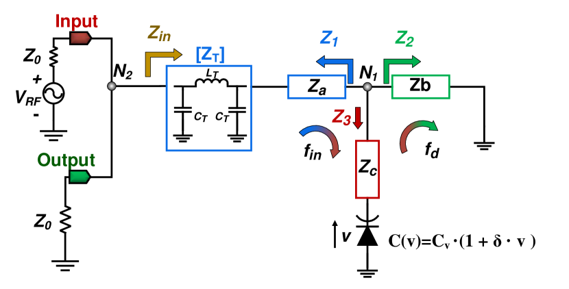
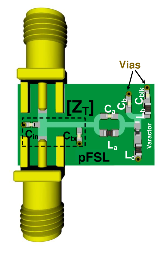
In the most simplistic representation, a reflective can be seen as a two-port passive network including one diode characterized by a biased capacitance and a corresponding tuning range (see Fig. 1), together with a set of components forming a stabilization network for the large signal periodic regimes excited in the circuit by . Without any loss of generality, we can assume any reflective to be representable through a T-network topology including the adopted diode, three one-port complex impedances ( , and ) and a quarter-wave transformer (labeled as []) with bandwidth centered around the value () of the input frequency (, corresponding to a natural frequency labeled as ) at which the minimum is desired. While the transformation stage can be implemented through any existing lumped or distributed circuit topologies, a third-order lumped implementation is assumed here in favor of a simpler analytical treatment. Also, such a two-port network, uniquely identified by an inductance () and a capacitance () setting the equivalent characteristic impedance , plays a key role to simultaneously achieve the lowest possible and values in , as it will be clear in the following section. Furthermore, to match the most frequent operational scenario, the same termination (, equal to 50 ) can be considered for the input and output ports. As the exhibited by needs to be as low as possible to ensure that even low power RXs characterized by a small dynamic range can be protected from EMI, it is crucial to find the optimal design specifications for [], , and (from now on labeled together as ) allowing to minimize the achievable . By relying on the same analytical methodology used to find the of PFDs in our recent theoretical investigation [23], the of the reflective shown in Fig. 1 can be found as:
12pt48pt
| (1) |
In (1), is the voltage level of the input generator with characteristic impedance equal to and power available equal to . Also, and represent the equivalent impedances seen at the half of the driving frequency (, equal to and corresponding to a natural frequency labeled as ) from node (see Fig. 1) towards and respectively, whereas is the equivalent impedance at seen from towards . Further, and [see (2) and (3) ] are complex functions of , , and of the impedances , and , where , and are the impedances seen at and from towards , and .
| (2) |
| (3) |
By replacing (2) and (3) in (1), it is straightforward to notice that the resulting expression is a function of all the impedances in the circuit (, , and the diode impedance) and of the first two coefficients of the linearized capacitance voltage characteristic of the biased diode (see Fig. 1). Moreover, since all the impedances in (1), (2) and (3) can be extracted through linear algorithms in any circuit simulators, their synthesis can be numerically tackled aiming at the minimization of without running time consuming nonlinear perturbation-based simulations, such as the ones available to investigate the steady-state large-signal operation of parametric circuits. Nevertheless, similarly to what we showed for PFDs in [23], the inspection of (1) after simplifying and with their corresponding expressions in (2) and (3) permits to realize that the minimum at can be attained by ensuring that four resonant conditions are satisfied: i) + must be in series resonance at with the lowest real part possible (); ii) + must be in series resonance at /2 with the lowest real part possible (); iii) must be in parallel resonance at with the highest real part possible; iv) must be in parallel resonance at /2 with the highest real part possible. In order to satisfy these resonance conditions through the use of a minimum number of lumped components, both and can be synthesized with parallel resonators, resonating at /2 and and relying on inductors (capacitors) with inductance (capacitance) () and () respectively. Furthermore, can be synthesized with one inductor whose inductance () is strategically selected to ensure the simultaneous validity of the first two resonant conditions, given the selected and values. Thus, when the resonant conditions mentioned above are satisfied, (1) can be simplified as:
| (4) |
where is equal to 2 and can be expressed in terms of [see (5)] when assuming for simplicity [] to be lossless.
| (5) |
In (5), captures the ohmic losses of both and along with the ones of the diode. Also, in the derivation of (4) we neglected the impact of and in favor of a simplified analytical treatment and an easier visualization of the main features determining in reflective . The validity of this approximation is granted by the fact that these two impedances, which are synthesized by two notches, just allow to isolate the signals at /2 and in dedicated meshes of the circuit. From (4) and (5) it is evident how the transformation stage plays a key role in lowering with respect to the value it would have (, +) if the resonant conditions were satisfied without using such a transformation stage. Therefore, the adoption of [] introduces fundamental means to reduce the lowest that can be attained by reflective . It is useful to simplify (4) by expressing and in terms of the quality factor of the diode (, relative to an value equal to ) and the ones ( and ) respectively exhibited at and /2 by + and +. Also, for operating in the Ultra-High-Frequency (UHF) range, like the prototype demonstrated in this work, we can assume to be equal to (, = , being dependent on the technology of the adopted passive components) and to be significantly higher than . This simplification is particularly valid when relying on diodes with wide tuning ranges, such as any available hyperabrupt varactors[33]. Consequently, can be considered equal to and can be simplified as follows:
| (6) |
| (7) |
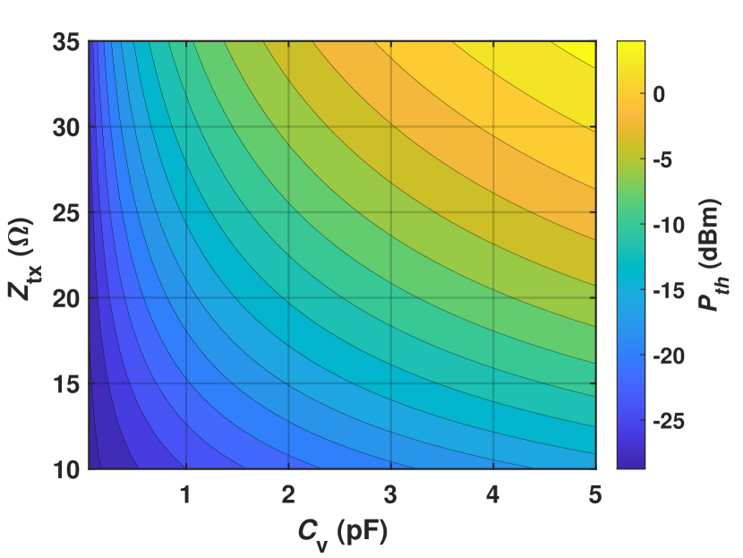
Equation (7) gives us the opportunity to estimate the minimum value that can be attained by reflective for any given of interest and for a chosen diode’s characteristics. As an example, we report a contour-plot capturing and [see (7)] in Fig. 2(a), which was analytically derived when assuming: i) the use of an hyperabrupt varactor (i.e., 0.4 and 15) with ranging from 50 fF to 5 pF, and ii) an of 2.1 GHz (in line with our experimental demonstration).
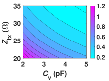
As evident from Fig. 2(a), reflective can achieve low values (0 dBm) through the strategic adoption of diodes with wide tuning range and low capacitance, along with /4 transformation stages characterized by the minimum realizable characteristic impedance. Nevertheless, since also need to exhibit the lowest possible insertion loss for power levels that are lower than , the selection of must also be made to ensure a minimum . In order to estimate the value of the shown in Fig. 1, we can extract the small-signal scattering parameter () for the transmission at from the ’s input port to the ’s output port, after linearizing the capacitance voltage characteristic of the diode around . The expression of in dB is provided in (8).
| (8) |
In (8), is the impedance seen at from the circuit node (see Fig. 1) towards and its value is almost independent of for <. Upon validity of the same resonance conditions that minimize and , it can be found that:
| (9) |
| (10) |
Equation (11) enables us to assess the minimum value that can be attained by reflective , given a selected value and based on the DC-biased capacitance of the selected diode. As an example, a contour-plot capturing and is displayed in Fig. 2(b), which was derived analytically while assuming the same , , and values used during the derivation of Fig. 2(a). By comparing (11) with (7) and Fig. 2(a) with Fig. 2(b), an important design trade-off between the desired and values can be identified. While relying on high- values allows to reduce , it also determines an increase of that can be unacceptable unless values in the -range were used. Since any board-level , such as the one we designed and built in this work, can only leverage values close to 1 pF or higher, there exists a fundamental limit for the minimum that can be obtained while preserving a low . Furthermore, cannot be made arbitrarily large without rendering [] severely affected by electrical loading, thus also degrading . This inevitably restraints the pool of usable diodes as it limits the maximum acceptable and consequently the minimum based on the maximum that can be tolerated. Therefore, the strategic selection of the diode and of the other components forming and is critical to make sure that the lowest can be attained without requiring a large that would compromise the achievable -value. Moreover, Fig. 2 provides useful means to assess the performance that would be achieved if were designed and built directly on-chip through any available CMOS technologies. In such a scenario, thanks to the availability of both capacitors and diodes with capacitance in the -range, any integrated reflective would be able to simultaneously rely on extraordinarily low and high values (1 k), thus enabling much lower values ( -20 dBm) than possible with board-level counterparts given a targeted value.
II-A Evaluation of the maximum value for a preserved frequency selectivity
While the achievement of low and values is certainly crucial, another metric to consider during the design of any is the maximum value ( , where is the corresponding peak voltage at ) at which a frequency selective attenuation at is preserved. In particular, with regards to reflective , the existence of a finite is due to periodic transitions from reverse to forward conduction that any diodes undergo when the voltage across their terminals exceeds the sum of the diode’s DC bias and built-in () voltages. Due to these transitions, the diode’s resistance () undergoes a sudden increase as is made larger than , leading to a progressive reduction of the parametrically generated negative resistance at responsible for the rising of the sub-harmonic oscillation in the circuit and, consequently, to a degradation of the performance at . As a first-order of approximation, can be found through a straightforward analysis of the circuit shown in Fig. 1 based on transmission matrices [see (12)] when assuming that , and satisfy the resonant conditions minimizing and when neglecting (for simplicity) any quadratic or cubic nonlinearities of the diode.
| (12) |
Equation (12) aids the selection of the diode by identifying the minimum allowing to preserve a frequency selective limiting behavior for values ranging from to any desired value, given any targeted and values. As an example, Fig. 3 shows a contour-plot capturing the analytically derived and [see (12)], assuming the same , and values used during the derivation of Fig. 2, a arbitrary set to 0.7 V (, the built-in voltage for silicon diodes) and a value of 2.0 pF [, the same used in our experimental demonstration when considering the additional parasitic capacitance (0.4 pF) associated to the diode’s package]. As evident from both (12) and Fig. 3, values lower than 0 dBm and fairly insensitive to are obtained with low capacitance diodes requiring the use of low values to operate. Nevertheless, significantly higher values can still be achieved by selecting larger diodes biased with higher DC voltages. By comparing (12) with (7), it can be noticed that represents the most important design parameter to ensure that high and low values can be achieved simultaneously. Furthermore, contrary to any reported absorptive counterparts, reflective are able to protect the integrity of any cascaded electronic components even for . Yet, within such high-power operative scenario, reflective progressively lose their frequency selectivity as is increased, thus ultimately showing strong attenuations across significant portions of their original bandwidth.
III Designing in Commercial Circuit Simulators
In the previous section, it has been shown how the achievement of the minimum and values in reflective can be ensured for any input frequencies of interest by satisfying four resonant conditions and by minimizing [see (11)]. Therefore, regardless of the nonlinear characteristics exhibited by , the synthesis of the passive impedances [i.e., [], , and (see Fig. 1)] forming any board-level reflective can be accomplished through linear simulation and optimization techniques, after selecting an available diode with the lowest possible and the highest possible , given the minimum tolerated value. It is worth pointing out that the capability to synthesize the different components of through linear methods enables the reliance on conventional algorithms during the optimization of both the ’ circuit and layout. Consequently, the optimal design conditions for any , including those operating at high frequency and consequently more impacted by layout parasitics, can be identified more reliably and more easily than what is possible when only relying on perturbation-based techniques. Nevertheless, such techniques are still required to assess the behavior of for , thus in the operative regime where the evolution of the circuit parameters strongly depends on the nonlinearities of the diode. Among the existing perturbation-based techniques, the power auxiliary generator (pAG[28]) technique provides unique means to extract the steady-state response of any parametric circuits without having to numerically enforce the validity of the non-perturbation condition[34] due to the adoption of an auxiliary generator in the circuit. A pAG consists of a continuous-wave (CW) voltage generator operating at and delivering a small non-perturbative power through a generator impedance (). When a pAG is used to simulate the response of a through a commercial Harmonic Balance (HB) circuit simulator, the pFSL’s output termination (i.e., in the circuit in Fig. 1) must be replaced by a pAG with also equal to . This allows to insert in the vector of frequencies that HB processors use to evaluate the response of driven RF circuits. In addition, by ensuring that matches , the adoption of the pAG does not cause variations of the impedance seen by the diode at or at multiples of , thus preventing any undesired changes in the dynamics of the circuit which would lead to unreliable predictions of the circuit’s response. The extraction of the steady-state response of can be achieved by sweeping from a much lower power than up to the maximum power level of interest, while configuring the values of the computed current and voltage phasors for any evaluated power level as initial conditions for the same circuit parameters prior the computation of the following data point to assess. Through this - sweeping strategy, it is possible to extract by evaluating the trend of the ’ insertion-loss for power levels exceeding . This also provides the means to fine-tune some of the component values synthesized in the earlier design stage towards the achievement of the highest value. In order to do so, it is convenient to look at (see Fig. 1) while varying some strategically selected circuit components to let the magnitude of this impedance be as small as possible for exceeding . During this design phase, the components synthesizing are the most adequate to be fine-tuned as they do not affect while only slightly altering . It is also important to point out that the ability to accurately predict in any is heavily influenced by the reliability of the available nonlinear circuit model for the adopted diode.
IV Experimental Results
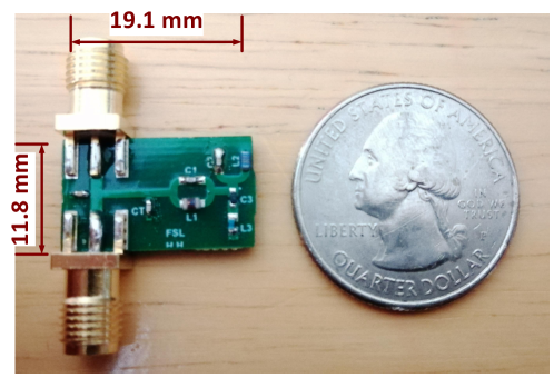
In order to demonstrate the capability of reflective to simultaneously exhibit low , low and high values, we designed a FR-4 Printed Circuit Board (PCB) implementation of a 2.1 GHz reflective (i.e., 2.1 GHz) using a commercial off-the-shelf hyperabrupt varactor (Skyworks SMV1231) as a diode. The assembled relies on a hybrid implementation of the circuit topology shown in Fig. 1, including a set of lumped components strategically selected together with the optimal geometrical layout characteristics (, the
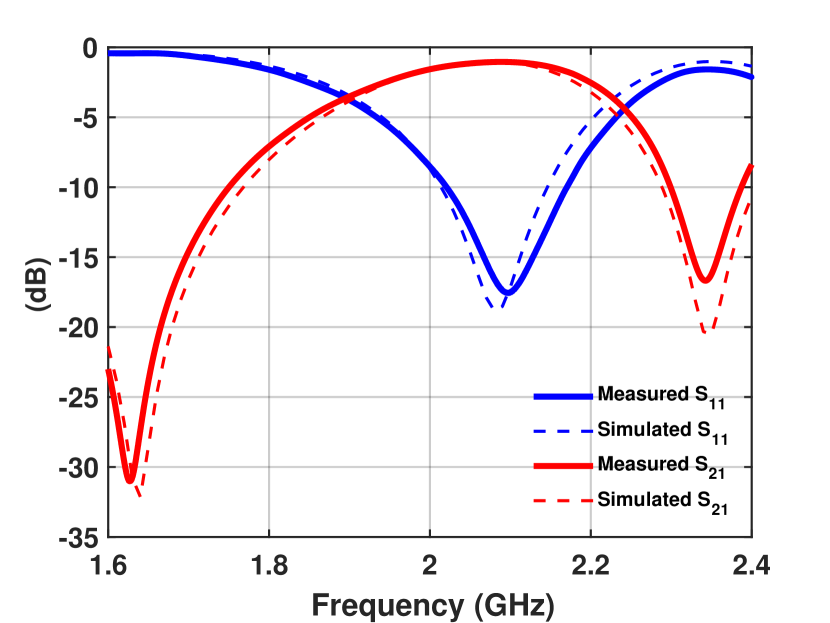
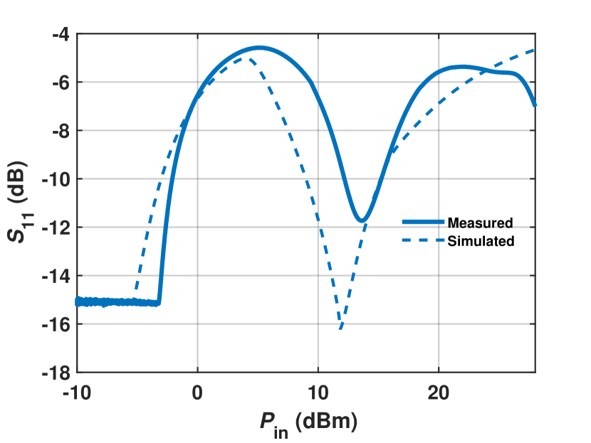
length and width of all interconnecting lines, the shape and foot-print of the selected surface-mount connectors, and the radius of each circular via). This allows to achieve a small form factor (2.2 of board area) and the lowest possible given an lower than a maximum tolerated value (here set to 1 dB). In particular, and were synthesized through two parallel resonators with inductors and , and capacitors and ; whereas was synthesized through an inductor () in series with the selected varactor. Also, a DC-blocking capacitor ( = 12 pF) was introduced in series with to permit the DC-biasing of the selected diode through a Bias-Tee (Inmet 8800SMF3-06) at the input port, even allowing an analog reconfigurability of and , as discussed later. The transformation stage at was designed to exhibit a value close to 31 when relying on two lumped capacitors ( and ) and two distributed inductors made of short lines. Such a value was chosen to ensure and values lower than -3 dBm and 1 dB respectively (see Fig. 2) based on the (2.0 pF) and (15) values exhibited by the varactor when is set to 1.1 V. Also, the adoption of distributed components in the transformation stage represents the most convenient design solution to ensure that the performance is not degraded by the capacitive coupling between the connectors’ foot-prints and the rest of the circuit, while preserving the lowest possible form-factor. The designed is visualized in Fig. 4 together with a photo of its built implementation, where the values and the model numbers of the selected lumped components are listed in the caption. The measured electrical response of the reported was first characterized through the extraction of its S-parameters for driving power levels (e.g., -30 dBm) much lower than the expected limiting threshold, thus in the operative regime where a linear operation can be assumed. Fig. 5 shows the resulting measured and closely matching simulated plots of the ’s and . Evidently, the reported exhibits a band-pass characteristic with a measured 3-dB fractional bandwidth (BW) of 17. Also, a minimum of 0.94 dB was measured for a frequency (2.06 GHz) close to the targeted . Such a record-low value closely matches both the corresponding circuit simulated one (0.9 dB) and our analytically derived expectation (0.6 dB, see Fig. 2(b)).
78pt28pt
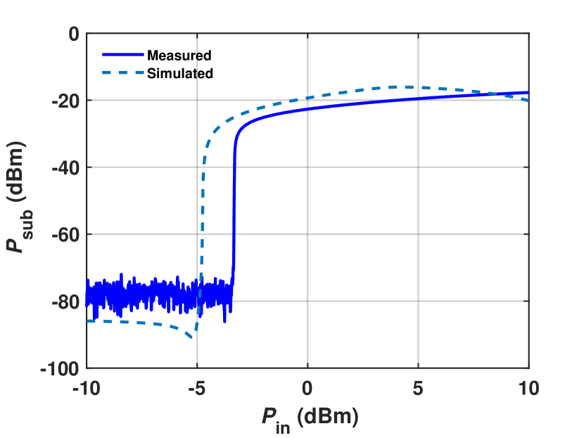
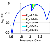
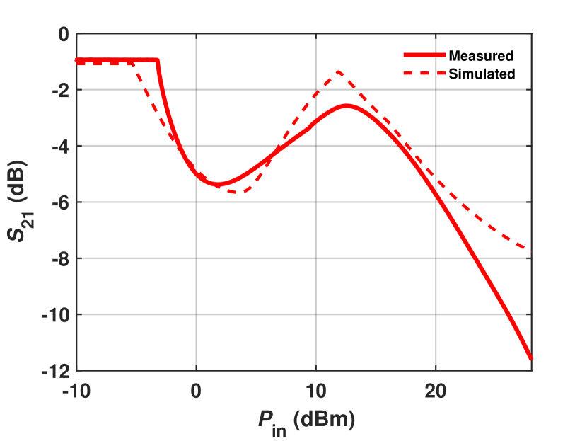
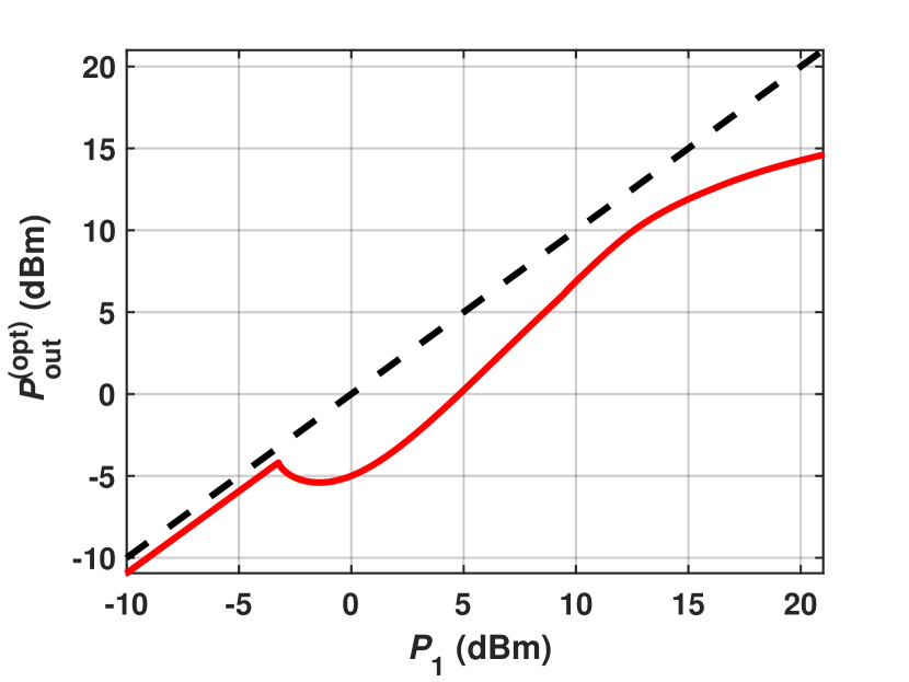
Later, we characterized the response for approaching and exceeding . In order to most reliably extract , we found the minimum value around 2.1 GHz triggering a 2:1 sub-harmonic oscillation in the circuit. In order to do so, we identified the power level at which a bifurcation triggering a 2:1 frequency division occurs from the measured output power (, see Fig. 6) at half of any explored driving frequencies. It is worth emphasizing that is not trivial only for exceeding . As shown in Fig. 6, the measured exhibits a minimum of -3.4 dBm at 2.06 GHz (, the same frequency minimizing , see Fig. 5). Such a measured value matches closely the predicted one found from the circuit simulated trend of (see the dotted line in Fig. 6). This simulated trend was obtained by utilizing the pAG technique and the extracted electromagnetic model (EM) of the designed board, together with the S-parameters of the selected lumped components. The measured is also close to its analytically predicted value (-4.8 dBm, see Fig. 2(a)), given the capacitance of the selected diode and the value chosen for . The value of the built at 2.06 GHz was assessed as well. This was done by extracting the corresponding for values ranging from -10 dBm to 28 dBm (the maximum available power level in our experiment, Fig. 7(a)). As evident, significant values up to 5.4 dB were found for and lower than 13 dBm. Within this power range, the designed shows a trend of the large-signal that realizes a frequency selective notch centered around 2.06 GHz, clearly indicating the activation of a frequency selective attenuation as is increased above (see the inset of Fig. 7(a)). Furthermore, despite its less frequency selective limiting behavior for , the measured shows high values even for higher than 13 dBm (12.0 dB for approaching 28 dBm). It is worth emphasizing that the achievement of such high value is granted by a parametrically triggered nonlinear mechanism causing the return-loss at the two ’s ports to significantly increase as is made larger than (see Fig. 7(b)).
83pt34pt
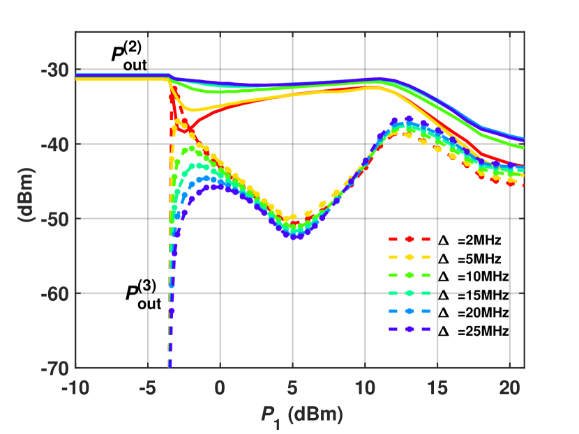
Nevertheless, both the measured and trends (Fig. 7) do not show a fully monotonic behavior, as also expected from the corresponding simulated trends (see the dotted lines in Fig. 7). This is due to changes in the diode’s dynamics becoming more and more significant as the input power approaches . In particular, through our circuit simulations, we found that the value associated with the local maximum (minimum) of the () for corresponds to a peak voltage level across the adopted diode equal to . This finding provided us with simple means to identify the value [13 dBm, close to its estimated analytical value (14 dBm, see Fig. 3)] of the built by extracting the level at which the same phenomenological change occurs in both the measured and trends. Finally, we evaluated the performance of the built when simultaneously driven by a 2.06 GHz signal and by a much lower power (-30 dBm) in-band tone. In order to do so, we relied on a conventional - harmonic test where two RF signals, combined through an external power combiner (Mini-Circuits ZFRSC-42-S+), were simultaneously injected in the circuit from the ’s input port. In particular, the signal at 2.06 GHz, with power labeled as , emulated the presence of a strong EMI at the ’s input port whereas the second much lower power signal (with -30 dBm), detuned from 2.06 GHz by an amount labeled as (, = 2.06 GHz+), was used to emulate the presence of a simultaneously received low-power signal carrying useful information. The output power levels at 2.06 GHz (), at () and the one () at the strongest -order intermodulation product ( = 4.12GHz-) were measured for levels ranging from -10 dBm to 21 dBm. It is crucial to emphasize that achieving low values is particularly important in applications where contiguous in-band channels with small frequency separations can be simultaneously received. The measured trends of , and are reported in Fig. 8(a) and Fig. 8(b) for values varying between 2 MHz and 25 MHz. It can be seen that the parametric mechanism responsible for the suppression of also causes an undesired attenuation () of that is higher for small values of (see Fig 8(b)). Yet, values not exceeding 2 dB and 4 dB were attained for values of 10 MHz and 5 MHz, thus demonstrating a good frequency selectivity in the limiting operation generated by the circuit. Also, values below -40 dBm were measured for values lower than and for higher than 10 MHz. It is key to point out that the ability to achieve such low values, regardless of the active parametrically triggered power limiting behavior, is due to the low impact exerted by the varactor’s quadratic nonlinearities on the circuit dynamics for power levels that are lower than . Nevertheless, for larger than the compressing and non-frequency-selective diode’s electrical response determines a saturation in the power level at all frequencies in the circuit, causing the observed behavior for 13 dBm. Ultimately, while the observation of has provided us with reliable means to quantify , the corresponding parametrically generated sub-harmonic signal, even if small, can also slightly degrade the signal-to-noise ratio () at the ’s output. Nevertheless, due to the large frequency separation between the ’s main operational frequency and its sub-harmonic one, a strong attenuation of can still be achieved through the adoption of a proper filtering stage at the output, without altering the circuit dynamics.
| Tech. | Component Area | ||||||
| [13] | Parametric | 4.5 | 3 | 850 | 9 | 3 dB* | n/a |
| [16] | Parametric | 10 | 3 | 2200 | 11 | 20 | n/a |
| [15] | Parametric | 3 | 3 | 2380 | 13 | 18 dB* | 9 |
| [14] | BSF | 3 | 2 | 1000 | 13 | n/a | 37 |
| [19] | BPF | 24 | 2 | 1500 | 10 | 10 | 378 |
| [18] | Coupler | 6 | 1.5 | 2000 | 8 | 12 | 3.5 |
| This work | Parametric | -3.4 | 0.94 | 2060 | 5.4 | 12.0 | 2.2 |
IV-A Threshold and frequency reconfigurability
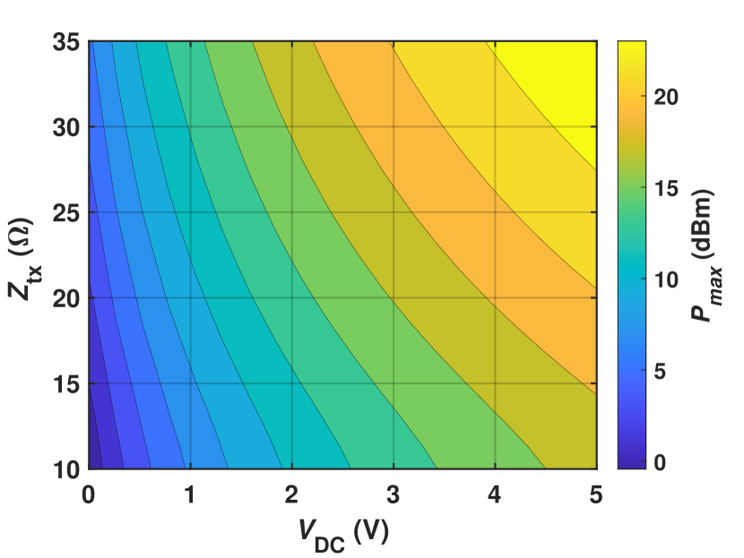
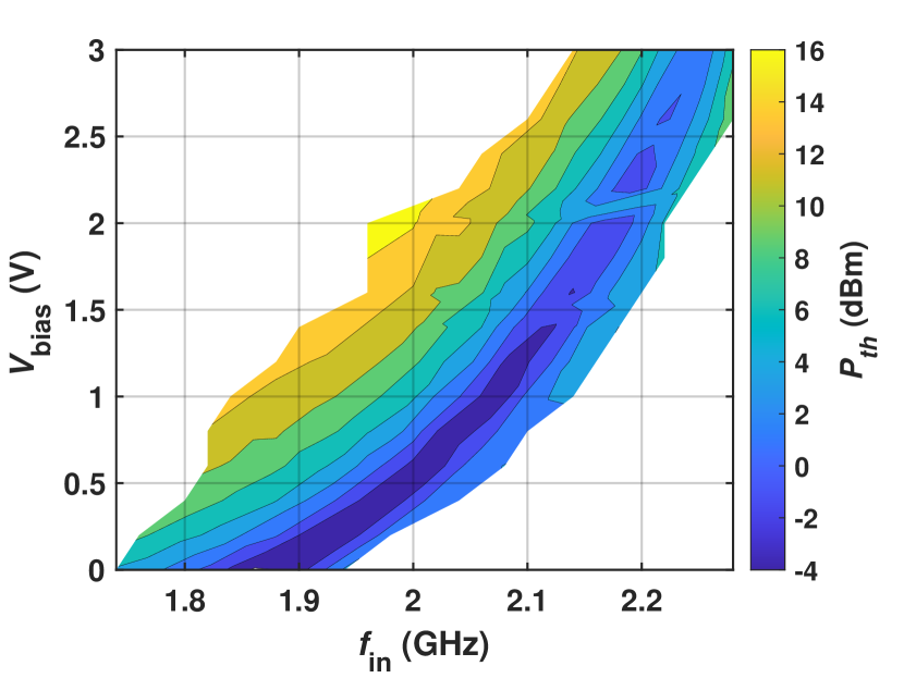
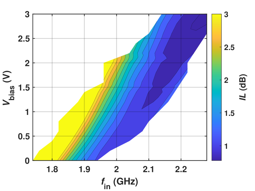
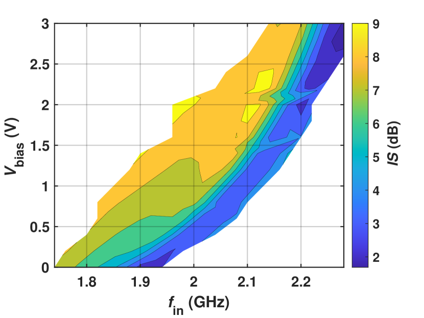
After characterizing the operation of the built at the value (1.1 V) resulting into the lowest around 2.1 GHz, we investigated the possibility to leverage different biasing conditions for the diode to reconfigure and the frequency at which the highest value is desired. Yet, to ensure that the built can be practically used to suppress EMI with different frequencies or power levels from the originally targeted value, we measured , and the maximum for () for a broad range of and values. This allowed us to construct three corresponding contour plots (see Fig. 9) capturing the value of each performance metric for the analyzed and values. As evident, through the strategic adoption of , the measured can simultaneously achieve and values lower than 2 dBm and 2 dB respectively, values up to 7 dB and a tunable operational frequency ranging from 1.85 GHz to 2.1 GHz.
IV-B Comparison with the State-of-the-Art
To benchmark the performance attained by our prototype with those attained by other passive diode-based FSLs, we compared (see Table I) the , , and of our built when is chosen to minimize with the corresponding values exhibited by the most recent demonstrated counterparts. Also, the value () of the reported for a much larger value (28 dBm) than was also compared to those of the other counterparts listed in Table I to assess the capability to protect any cascaded electronic components even from exceptionally strong EMI. As evident from Table I, the reported in this work exhibits the lowest and values among all the previously demonstrated diode-based passive FSLs, even though it is operating at one of the highest frequencies. In particular, the value attained by our reported is nearly five times lower than what achieved by the previously reported SoA counterparts operating within the same frequency range. Nevertheless, when is selected to minimize , is lower than what shown by the other previously reported diode-based FSLs. Yet, as shown in Fig. 9, can be increased up to 7 dB by relying on slightly different values, at the cost of higher (still lower than 2 dBm) and (still lower than 2 dB). Furthermore, it is important to point out that, differently from other listed prototypes, the reported exhibits a large exceeding 12.0 dB, limiting the maximum output power delivered to any cascaded components to 13 dBm even in those scenarios when strong EMI with power approaching 30 dBm is received. Finally, by looking at the reported area of all the FSLs listed in Table I, it is easy to notice that our reported shows the highest degree of miniaturization.
In the next section an alternative approach not relying on changes of is introduced and experimentally validated to enhance both and without significantly degrading and while preserving record-low values (2 dB).
20pt34pt
IV-C Increasing through multiple stages
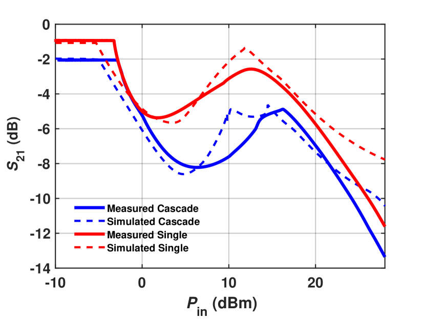
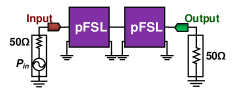
Similarly to what was previously shown for absorptive [13], cascading multiple reflective provides useful means to increase , augmenting the maximum achievable suppression at . Nevertheless, this technique can be practically leveraged only when absorptive or reflective with low are available, such as the one we designed and built in this work. In fact, since the insertion-loss of a chain of () grows proportionally with the number of cascaded stages (), there exists an inevitable trade-off between the maximum exploitable and the highest tolerated . Also, differently from any chains of absorptive whose design and operation inevitably lead to values increasing proportionally to , the high (see Fig. 1) value exhibited by reflective for renders the voltage at across all the adopted diodes almost independent of , especially when is chosen to be much higher than in order to minimize . This key operational feature allows to preserve low values even when multiple reflective stages are used to enable higher . Moreover, contrary to absorptive , the adoption of multiple reflective stages permits to increase even the values attained for much higher values than .
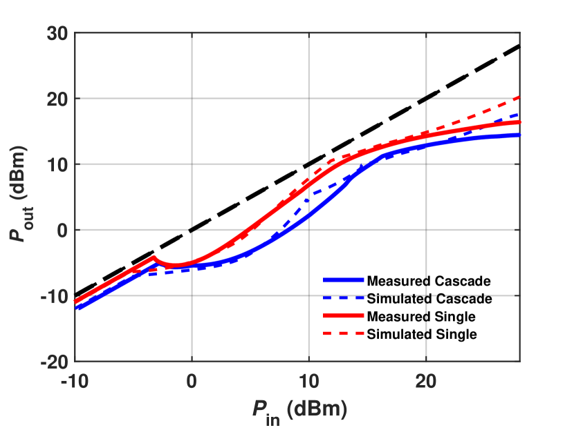
In order to demonstrate the capability to achieve higher values through the adoption of multiple stages, we built a copy of the discussed in the previous section. The two were then connected to each other and the modified trends of the were extracted (Fig. 10(a)), along with the corresponding trend of the output power at 2.06 GHz (, the value giving the lowest threshold for a single stage ). As evident from Fig. 10, the chain formed by the two built stages allows to significantly enhance the maximum value attained by just one stage, while causing negligible (1 dB) increases of and .
V Conclusion
In this article, we discussed the design criteria and measured performance of a 2.1 GHz diode-based reflective parametric frequency selective limiter () built on a FR-4 printed-circuit-board (PCB) and using commercial off-the-shelf components. Thanks to its engineered dynamics, the reported prototype can exhibit record-low insertion-loss for low-power signals (, as low as 0.94 dB), record-low power threshold (, as low as -3.4 dBm) and a significant suppression (up to 5.4 dB) for input power levels lower than the one forcing the diode to operate in its forward conduction. Furthermore, due to its unique design characteristics and regardless of the inevitable reduction in frequency selectivity, the built ensures a good protection even from much stronger interference signals with power approaching 28 dBm. In addition, by strategically tuning the DC-biasing voltage of the diode, the reported allows to reconfigure the frequency at which the maximum is obtained by nearly 250 MHz (corresponding to a tuning range of 0.12 ), while simultaneously preserving low (2 dBm) and ( 2 dB) values. Finally, by connecting two copies of the same designed and built in this work, we demonstrated that a significantly larger suppression value (8 dB) for high-power signals can be attained, while preserving low (-2.5 dBm) and low (2 dB).
Acknowledgment
This work has been funded by the National Science Foundation (NSF) under award #1854573.
References
- [1] R. Orth, “Frequency-selective limiters and their application,” vol. EMC-10, pp. 273–283, 1968.
- [2] K. L. Kotzebue, “Frequency-selective limiting,” IRE Transactions on Microwave Theory and Techniques, vol. 10, no. 6, pp. 516–520, 1962.
- [3] A. J. Giarola, “A review of the theory, characteristics, and operation of frequency selective limiters,” Proceedings of the IEEE, vol. 67, no. 10, pp. 1380–1396, 1979.
- [4] D. R. Jackson and R. W. Orth, “A frequency-selective limiter using nuclear magnetic resonance,” Proceedings of the IEEE, vol. 55, no. 1, pp. 36–45, 1967.
- [5] A. Berman, “Multiple-carrier behavior of a frequency-selective ferrite limiter,” IEEE Transactions on Communications Systems, vol. 12, no. 2, pp. 138–150, 1964.
- [6] S. N. Stitzer and H. Goldie, “A multi-octave frequency selective limiter,” in Proc. IEEE MTT-S Int. Microwave Symp. Digest, 1983, pp. 326–328.
- [7] J. D. Adam and S. N. Stitzer, “Frequency selective limiters for high dynamic range microwave receivers,” IEEE Transactions on Microwave Theory and Techniques, vol. 41, no. 12, pp. 2227–2231, 1993.
- [8] S. N. Stitzer, “Spike leakage and suppression in frequency selective limiters,” in Proc. IEEE MTT-S Int. Microwave Symp. Digest (Cat. No.00CH37017), vol. 2, 2000, pp. 901–904 vol.2.
- [9] J. D. Adam and S. N. Stitzer, “Msw frequency selective limiters at UHF,” IEEE Transactions on Magnetics, vol. 40, no. 4, pp. 2844–2846, 2004.
- [10] J. D. Adam and F. Winter, “Magnetostatic wave frequency selective limiters,” IEEE Transactions on Magnetics, vol. 49, no. 3, pp. 956–962, 2013.
- [11] T. R. Billeter, “Epr frequency-selective limiter,” Proceedings of the IEEE, vol. 56, no. 3, pp. 370–371, 1968.
- [12] S. M. Gillette, M. Geiler, J. D. Adam, and A. L. Geiler, “Ferrite-based reflective-type frequency selective limiters,” IEEE MTT-S International Microwave Workshop Series on Advanced Materials and Processes for RF and THz Applications, 2018.
- [13] F. Ramirez, R. Melville, A. Suarez, and J. S. Kenney, “Nonlinear analysis and design of frequency selective limiters based on parametric circuits,” in Proc. IEEE MTT-S Int. Microwave Symp. Digest, 2008, pp. 947–950.
- [14] P. Phudpong and I. C. Hunter, “Frequency-selective limiters using nonlinear bandstop filters,” IEEE Transactions on Microwave Theory and Techniques, vol. 57, no. 1, pp. 157–164, 2009.
- [15] I. T. Ho and A. E. Siegman, “Passive phase-distortionless parametric limiting with varactor diodes,” IRE Transactions on Microwave Theory and Techniques, vol. 9, no. 6, pp. 459–472, 1961.
- [16] A. Wolf and J. Pippin, “A passive parametric limiter,” in Proc. IEEE Int. Solid-State Circuits Conf.. Digest of Technical Papers, vol. III, 1960, pp. 90–91.
- [17] P. Phudpong and I. C. Hunter, “Nonlinear matched reflection mode bandstop filters for frequency selective limiting applications,” in Proc. IEEE/MTT-S Int. Microwave Symp, 2007, pp. 1043–1046.
- [18] A. Hueltes, E. Rocas, C. Collado, J. Mateu, N. Orloff, J. C. Booth, D. Garcia-Pastor, and R. Perea-Robles, “Three-port frequency-selective absorptive limiter,” IEEE Microwave and Wireless Components Letters, vol. 27, no. 5, pp. 479–481, 2017.
- [19] E. J. Naglich and A. C. Guyette, “Frequency-selective limiters utilizing contiguous-channel double multiplexer topology,” IEEE Transactions on Microwave Theory and Techniques, vol. 64, no. 9, pp. 2871–2882, 2016.
- [20] W. Yang, M. Abu Khater, E. J. Naglich, D. Psychogiou, and D. Peroulis, “Frequency-selective limiters using triple-mode filters,” IEEE Access, vol. 8, pp. 114 854–114 863, 2020.
- [21] C. Cassella, S. Strachan, S. W. Shaw, and G. Piazza, “Phase noise suppression through parametric filtering,” Applied Physics Letters, vol. 110, no. 6, p. 063503, 2017.
- [22] C. Cassella, N. Miller, J. Segovia-Fernandez, and G. Piazza, “Parametric filtering surpasses resonator noise in aln contour-mode oscillators,” in Proc. IEEE 27th Int. Conf. Micro Electro Mechanical Systems (MEMS), 2014, pp. 1269–1272.
- [23] H. M. E. Hussein, M. A. A. Ibrahim, G. Michetti, M. Rinaldi, M. Onabajo, and C. Cassella, “Systematic synthesis and design of ultralow threshold 2:1 Parametric frequency dividers,” IEEE Transactions on Microwave Theory and Techniques, vol. 68, no. 8, pp. 3497–3509, 2020.
- [24] H. M. E. Hussein, M. Rinaldi, M. Onabajo, and C. Cassella, “Chip-less and battery-less subharmonic tags for wireless sensing with parametrically enhanced sensitivities and dynamic ranges,” Research Square, 2020, available online: https://www.researchsquare.com/article/rs-81763.
- [25] C.-H. Chang and M. Onabajo, “Analysis and demonstration of an IIP3 improvement technique for low-power rf low-noise amplifiers,” IEEE Transactions on Circuits and Systems I: Regular Papers, vol. 65, no. 3, pp. 859–869, 2018.
- [26] L. Xu, C. Chang, and M. Onabajo, “A 0.77 mw 2.4 ghz rf front-end with 4.5 dbm in-band IIP3 through inherent filtering,” IEEE Microwave and Wireless Components Letters, vol. 26, no. 5, pp. 352–354, 2016.
- [27] G. Jha, M. A. A. Ibrahim, and M. Onabajo, “A low-power complex bandpass gm-c filter with dynamic range expansion through adaptive biasing,” in Proc. IEEE Intl. Symp. on Circuits and Systems (ISCAS), 2018.
- [28] C. Cassella and G. Piazza, “Low phase-noise autonomous parametric oscillator based on a 226.7 MHz AlN contour-mode resonator,” and Frequency Control IEEE Transactions on Ultrasonics, Ferroelectrics, vol. 62, no. 4, pp. 617–624, 2015.
- [29] L. Pantoli, A. Suarez, G. Leuzzi, and F. Di Paolo, “Complete and systematic simulation tools for frequency divider design,” IEEE Transactions on Microwave Theory and Techniques, vol. 56, no. 11, pp. 2442–2452, 2008.
- [30] M. Pontón and A. Suárez, “Analysis of a frequency divider by two based on a differential nonlinear transmission line,” in Proc. IEEE MTT-S Int. Microwave Symp, 2015, pp. 1–3.
- [31] A. Suárez and F. Ramírez, “Stability and bifurcation analysis of multi-element non-foster networks,” IEEE Transactions on Microwave Theory and Techniques, vol. 66, no. 4, pp. 1817–1830, 2018.
- [32] S. Hernández and A. Suárez, “Systematic methodology for the global stability analysis of nonlinear circuits,” IEEE Transactions on Microwave Theory and Techniques, vol. 67, no. 1, pp. 3–15, 2019.
- [33] M. P. J. Tiggelman, K. Reimann, F. Van Rijs, J. Schmitz, and R. J. E. Hueting, “On the trade-off between quality factor and tuning ratio in tunable high-frequency capacitors,” IEEE Transactions on Electron Devices, vol. 56, no. 9, pp. 2128–2136, 2009.
- [34] A. Suárez, Analysis and design of autonomous microwave circuits. John Wiley & Sons, 2009, vol. 190.
![[Uncaptioned image]](/html/2012.11546/assets/Figures/Hussein.png) |
Hussein M. E. Hussein (S’20) received his B.S. and M.Sc. in electrical engineering at Cairo University, Giza, Egypt, in 2013 and 2017, respectively. He is currently pursuing the Ph.D. degree with the Electrical and Computer Engineering department at Northeastern University, Boston, MA, USA. He is currently working on the development of parametric phase noise reduction techniques, for RF systems, based on nonlinear devices and circuits. |
![[Uncaptioned image]](/html/2012.11546/assets/Figures/Mahmoud.png) |
Mahmoud A. A. Ibrahim
(S’13) received the B.Sc. (Hons.) and M.Sc. degrees in electrical engineering from the Electronics and Electrical Communications Engineering Department, Cairo University, Giza, Egypt, in 2013 and 2015, respectively. He is currently pursuing the Ph.D. degree in electrical engineering with Northeastern University, Boston, MA, USA.
From 2013 to 2015, he was a Teaching and Research Assistant with Cairo University. In the summer of 2018, he joined the PLL Team at Qualcomm, San Diego, CA, USA, as an Analog-Mixed Signal Design Intern; where he was involved in the research and design of ultra-low power multi-Giga Hertz LC-oscillators in deep-submicron Fin-FET technologies. Since 2016, he has been a Graduate Research and a Teaching Assistant with Northeastern University. He is also working on the design of ultra-low power transceivers for biomedical applications. His research interests include integrated analog, mixed-signal, RF circuits for low-power wireless transceivers, and power management integrated circuits. |
![[Uncaptioned image]](/html/2012.11546/assets/Figures/Matteo.png) |
Matteo Rinaldi is a Professor in the Electrical and Computer Engineering department at Northeastern University and the Director of Northeastern SMART a university research center that, by fostering partnership between university, industry and government stakeholders, aims to conceive and pilot disruptive technological innovation in devices and systems capable of addressing fundamental technology gaps in several fields including the Internet of Things (IoT), 5G, Quantum Engineering, Digital Agriculture, Robotics and Healthcare. Dr. Rinaldi received his Ph.D. degree in Electrical and Systems Engineering from the University of Pennsylvania in December 2010. He worked as a Postdoctoral Researcher at the University of Pennsylvania in 2011 and he joined the Electrical and Computer Engineering department at Northeastern University as an Assistant Professor in January 2012. Dr. Rinaldi’s group has been actively working on experimental research topics and practical applications to ultra-low power MEMS/NEMS sensors (infrared, magnetic, chemical and biological), plasmonic micro and nano electromechanical devices, medical micro systems and implantable micro devices for intra-body networks, reconfigurable radio frequency devices and systems, phase change material switches, 2D material enabled micro and nano mechanical devices. The research in Dr. Rinaldi’s group is supported by several Federal grants (including DARPA, ARPA-E, NSF, DHS), the Bill and Melinda Gates Foundation and the Keck Foundation with funding of $14+M since 2012. Dr. Rinaldi has co-authored more than 140 publications in the aforementioned research areas and also holds 10 patents and more than 10 device patent applications in the field of MEMS/NEMS. Dr. Rinaldi was the recipient of the IEEE Sensors Council Early Career Award in 2015, the NSF CAREER Award in 2014 and the DARPA Young Faculty Award class of 2012. He received the Best Student Paper Award at the 2009, 2011, 2015 (with his student) and 2017 (with his student) IEEE International Frequency Control Symposiums; the Outstanding Paper Award at the 18th International Conference on Solid-State Sensors, Actuators and Microsystems, Transducers 2015 (with his student) and the Outstanding Paper Award at the 32nd IEEE International Conference on Micro Electro Mechanical Systems, MEMS 2019 (with his student). Prof. Rinaldi is the founder and CEO of Zepsor Technologies, a start-up company that aims to bring to market zero standby power sensors for various internet of things applications including distributed wireless fire monitoring systems, battery-less infrared sensor tags for occupancy sensing and distributed wireless monitoring systems of plant health parameters for digital agriculture. Prof. Rinaldi is also the owner of Smart MicroTech Consulting LLC, a company that routinely provides consulting services to government agencies, large companies and startups in the broad areas of Micro and Nano Technologies, Internet of Things, Wireless Communication devices and systems, Radio Frequency Devices and Systems and Sensors. |
![[Uncaptioned image]](/html/2012.11546/assets/Figures/Marvin.jpg) |
Marvin Onabajo (S’01–M’10–SM’14) is an Associate Professor in the Electrical and Computer Engineering Department at Northeastern University. He received a B.S. degree (summa cum laude) in Electrical Engineering from The University of Texas at Arlington in 2003, as well as the M.S. and Ph.D. degrees in Electrical Engineering from Texas A&M University in 2007 and 2011, respectively. From 2004 to 2005, he was Electrical Test/Product Engineer at Intel Corp. in Hillsboro, Oregon. He joined the Analog and Mixed-Signal Center at Texas A&M University in 2005, where he was engaged in research projects involving analog built-in testing, data converters, and on-chip temperature sensors for thermal monitoring. In the spring 2011 semester, he worked as a Design Engineering Intern in the Broadband RF/Tuner Development group at Broadcom Corp. in Irvine, California. Marvin Onabajo has been at Northeastern University since the Fall 2011 semester. His research areas are analog/RF integrated circuit design, on-chip built-in testing and calibration, mixed-signal integrated circuits for medical applications, data converters, and on-chip sensors for thermal monitoring. He currently serves as Associate Editor on the editorial boards of the IEEE Transactions on Circuits and Systems I (TCAS-I, 2016-2017, 2018-2019, and 2020-2021 terms) and of the IEEE Circuits and Systems Magazine (2016-2017, 2018-2019, and 2020-2021 terms). During the 2014-2015 term, he was on the editorial board of the IEEE Transactions on Circuits and Systems II (TCAS-II). He received a 2015 CAREER Award from the National Science Foundation, a 2017 Young Investigator Program Award from the Army Research Office (ARO), and the 2015 Martin Essigman Outstanding Teaching Award from the College of Engineering at Northeastern University. |
![[Uncaptioned image]](/html/2012.11546/assets/Figures/cassella.jpg) |
Cristian Cassella is an Assistant Professor in the Electrical and Computer Engineering department at Northeastern University, Boston (USA). He received his B.S.E. and M.Sc., with honors, at University of Rome – Torvergata in 2006 and 2009, respectively. In 2011, he was a visiting scholar at University of Pennsylvania. In 2012 he entered a Ph.D. program at Carnegie Mellon University which he completed in 2015. In 2015 he was a Postdoctoral Research Associate at Northeastern University. In 2016, he became Associate Research Scientist. He is author of 80 publications in peer-reviewed journals and conference proceedings. Two of his peer-reviewed journal papers published on the IEEE Journal of MicroElectroMechanical systems (JMEMS) were selected as papers of excellent quality (JMEMS RightNowPapers), hence being released as open-access. One of his journal papers was chosen as the cover for the Nature Nanotechnology October 2017 issue. An other one of his journal papers was selected as a featured article by the Applied Physics Letters magazine. He won the best paper award at the IEEE International Frequency Control Symposium (2013, Prague). In 2018, he was awarded by the European Community (EU) the Marie-Sklodowska-Curie Individual Fellowship. He holds four patents and four patent applications in the area of acoustic resonators and RF systems. He is a technical reviewer for several journals, such as Applied Physics Letter, IEEE Transactions on Electron Devices, IEEE Transactions on Ultrasound, Ferroelectric and Frequency Control, IEEE Journal of MicroElectroMechanical devices, IEEE Electron Device Letter, Journal of Micromachine and Micro-Engineering, Journal of Applied Physics, IEEE Sensors Letter and Review of Scientific Instruments. |