The Upgrade of the CMS Tracker at HL-LHC
Abstract
In the high luminosity scenario of the LHC (HL-LHC), which will bring the instantaneous luminosity up to 7.5 cm-2s-1, ATLAS and CMS will need to operate at up to 200 interactions per 25 ns beam crossing and reaching up to 4000 fb-1 of integrated luminosity. To achieve their physics goals the experiments will need to improve the tracking and vertexing capability and the ability to selectively trigger on specific physics events at reasonable thresholds. The upgrade of the CMS Tracker requires designing new inner and outer tracking detectors to cope with the increased luminosity and to implement first trigger level functionality. This paper describes the new layout and the technological choices together with some highlights of research and development activities.
1 Introduction
The High-Luminosity Large Hadron Collider (HL-LHC [1]) at CERN is expected to collide protons at a centre-of-mass energy of 14 TeV and to reach the unprecedented peak instantaneous luminosity of 7.5 x cm-2s-1 with an average number of pileup interactions up to 200. This will allow the ATLAS [2] and CMS [3] experiments to collect integrated luminosities of 3000 fb-1 during the project baseline lifetime, with the possibility to reach 4000 fb-1 as ultimate scenario. To cope with this very challenging scenario the CMS detector will be substantially upgraded [4] before the start of the HL-LHC. The CMS tracking detector will have to be replaced in order to fully exploit the delivered luminosity and cope with the demanding operating conditions. The new detector will provide robust tracking as well as input for the first level trigger (L1).
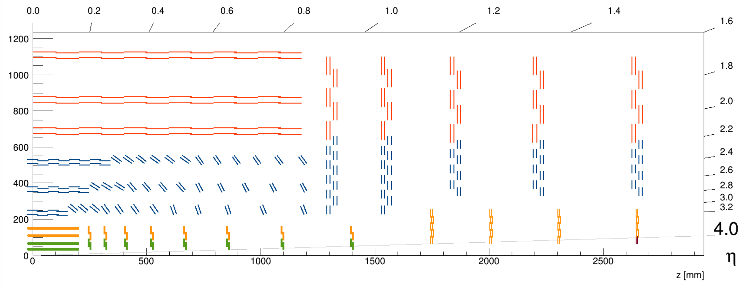
The CMS Phase-2 tracker will consist of about 200 m2 of silicon modules and will be composed of two sub-detectors: the Inner Tracker (IT) made of silicon pixel modules and the Outer Tracker (OT) made of a combination of silicon modules with strip and macro-pixel sensors. A longitudinal view of one quarter of the new detector layout is shown in Fig. 1.
The main requirements for the new tracker can be summarised as follows: radiation tolerance to be fully efficient up to the expected integrated luminosity; increased granularity to ensure excellent tracking performance in the presence of a high level of pileup (occupancy less than 1% for the OT and 0.1% for the IT); reduced material in the tracking volume; contribution of tracking information to the L1 trigger (only for OT); large readout bandwidth and deep front-end buffers for higher rate (750 kHz) and longer latency (12.5 s) of the L1 trigger system; extended tracking acceptance up to 4 for efficient pile-up mitigation and better track reconstruction in the forward region.
2 Inner Tracker system
The Inner Tracker consists of four barrel layers (TBPX) plus eight small disks (TFPX) and four large disks (TEPX) per side, covering a surface of 5 m2 with 3900 hybrid pixel modules featuring about 2 billion readout channels. In addition to extending the tracking acceptance up to 4, the TEPX disks are employed to perform real time luminosity measurements. The innermost rings of the outermost TEPX disks are exclusively used for beam background and luminosity measurements with independent readout and control systems. The expected hadron fluences and total ionising dose for the innermost pixel layer are 3.5 neq cm-2 and 1.9 Grad, respectively. A replacement of the innermost pixel layer and the innermost ring of the TFPX will be required during the long shutdown (LS) number 5 of the current HL-LHC schedule, irrespective of which sensor technology will be selected.
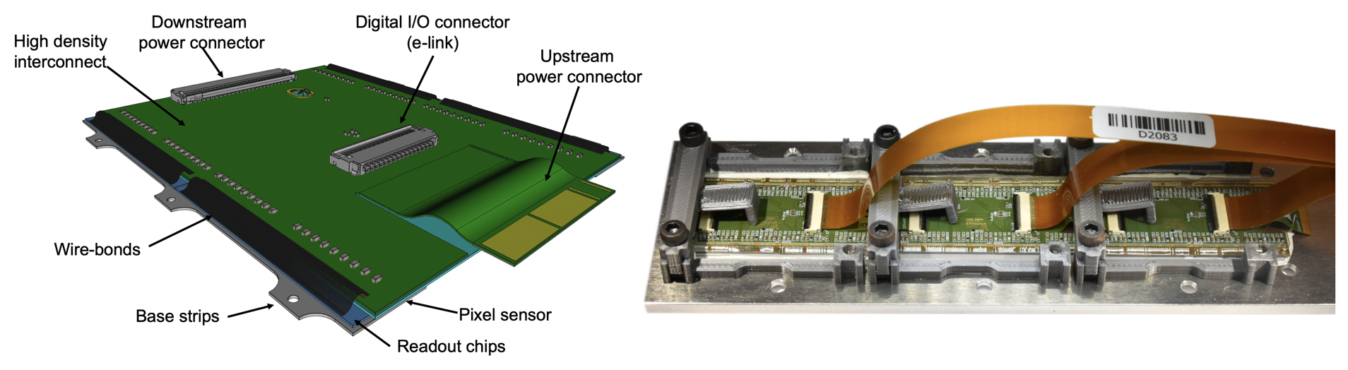
The basic units of the IT detector are the hybrid pixel modules. As shown in Fig. 1, two types of pixel modules will be employed in the detector: 1 2 (green) and 2 2 (yellow) readout chips (ROC) per sensor. The module consists of ROCs bump-bonded onto the sensor that is glued on a High-Density-Interconnect flexible PCB (HDI). The connection between the ROCs and HDI is made via wire-bonds and the ROCs are mounted on aluminum nitride base strips as Fig. 2 shows. The HDI is designed to provide a return supply current path and for low material budget. It is equipped only with power and readout connectors and passive components used for setting some of the ROCs operational parameters.
An extensive silicon pixel sensors R&D for qualifying sensors capable to operate up to the neq cm-2 range is currently on-going and 150 m thick n-in-p planar sensors are the current baseline for the IT detector. In order to guarantee a consistent charge collection efficiency after irradiation the technology requires a high bias voltage up to 1 kV. Due to the sensor structure and the high voltage presence in the proximity to the ROC, a spark protection between the two components is required. A dedicated R&D on the use of a combination of three types of dielectric protection (BenzoCycloButene layer on sensor edges, polyimide layer on ROC periphery and parylene coating at module level) started in 2019 and a reliability study after irradiation is currently on-going with the target to converge to a solution at the end of 2020. An alternative for the inner layers of the TBPX is the 3D silicon sensor technology, which is more radiation hard and requires lower bias voltages. The 3D technology has the disadvantage of having a larger pixel capacitance and a more complex fabrication process with a lower yield.
Two possible pixel sizes are being considered: 25 100 m2, as current baseline, and 50 50 m2. Initial studies show that, the relative difference in term track parameter resolution between the two designs is rather small with a trade-off between primary vertex discrimination and resolution on the impact parameter. For the innermost layer, square pixels would result in a very long cluster which would set more stringent requirements on the operational threshold of the chip, and it would also demand a larger bandwidth for reading the data.
The readout chip for the ATLAS and CMS pixel detectors at HL-LHC is under design by the CERN RD53 collaboration [5]. The chip, designed in 65 nm CMOS technology, has been developed with a cell size of 50 50 m2, a low threshold (below 1000 e-), a high data rate (one 160 Mb/s input link and up to four 1.28 Gb/s output links) and serial powering capability. The first half-size prototype chip, RD53A [6], featured a 400 192 pixel matrix and has been used for extensive R&D and qualification programs by ATLAS and CMS. Radiation hardness up to 500 Mrad was proven with indications that operation up to 1 Grad would be possible under controlled conditions, most importantly by cooling the chip during the full lifetime. In the RD53A chip, three different analogue front-ends (FE) are prototyped in three sub-matrices. These are the synchronous FE, linear FE and differential FE. After a dedicated review process CMS has selected the linear FE for the final chip. The common design framework of the final chip, known as RD53B, contains design improvements and a few fixed bugs identified in the RD53A. A dedicated overview of the qualification results is given in [7]. The CMS final chip size is 16.8 21.6 mm2 with a matrix of 336 432 pixels. The submission of the first full size chip prototype for CMS is expected at the end of 2020.
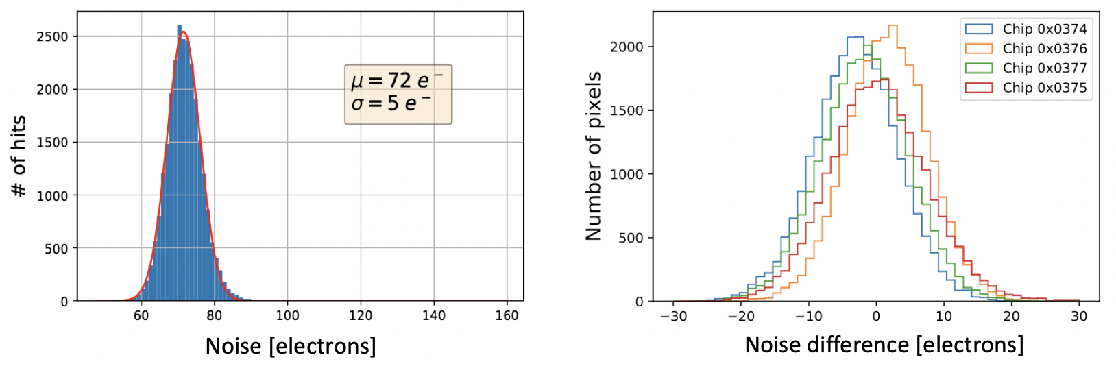
The extreme rate requirements for the readout chip necessitate the use of a CMOS technology with low supply voltage (1.2 V), resulting in a chip that must be supplied with significant current levels (2 A per chip). It has been calculated that the total needed power for the Inner Tracker is around 50 kW. The use of a standard detector powering schema that has all readout chips supplied in parallel with a constant voltage is not possible, due to the voltage drop along the cables and the prohibitively large cable cross section that would be required. Similarly point-of-load-DCDC conversion cannot be employed due to space constraints. The only viable powering scheme for such an environment is serial distribution. In this scheme 8 to 12 modules are arranged in a chain. All chain elements receive the same current and the voltage is equally shared if all elements represent the same and constant load. This is possible due to the ShuntLDO implementation in the readout chip that combines a linear regulator (LDO) and a shunt. A picture of a serially powered chain of three digital modules is shown in Fig. 2, while Fig. 3 shows the noise distribution of a module in standalone operation and the chip by chip difference after inclusion in the serial chain [8].
The IT modules will be connected with up to 1.6 m electrical links to optical-modules located at the periphery of the detector. The optical module hosts two LpGBT [9] transceivers and two VTRx+ [10] optical links. In total six 1.28 Gb/s up-links per module will be implemented for data and monitoring information, and one 160 Mb/s down-link for bringing clock, trigger, fast commands and configuration data to the module.
3 Outer Tracker system
The Outer Tracker consists of six barrel layers and five endcap disks per end, and it is subdivided in: TB2S (Tracker Barrel with 2S modules), TBPS (Tracker Barrel with PS modules) and two TEDDs (Tracker Endcap Double Disks). The OT covers a surface of 190 m2 with 13’200 modules featuring about 213 million of readout channels.
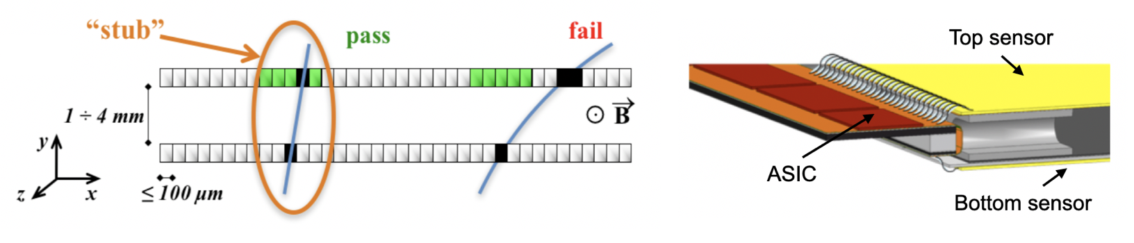
The modules have the ability to autonomously select track segments (stubs) above a selected pT threshold and to send these to the backend electronics. The selection relies on the bending of the charged particles in the magnetic field and a programmable selection window in the readout chips (see Fig. 4). The backend track finder system receives the stub data from the individual detector modules and performs track finding in two steps, pattern recognition and track fitting, and sends the final tracks to the L1 trigger [4].
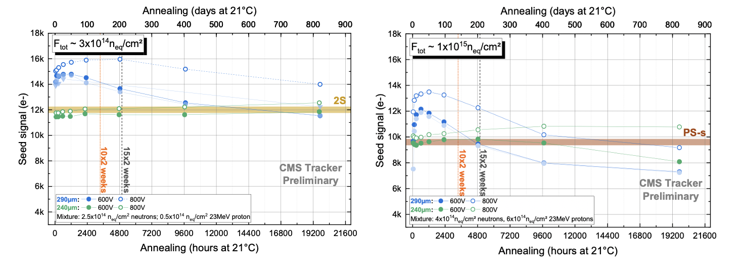
An extensive R&D was undertaken to identify the sensor technology for the OT. At the end, only two options were left: Float Zone (FZ) silicon n-in-p with an active sensor thickness of 290 m (FZ290) or 240 m (FZ240). The sensor technology chosen for both sensors of the pT modules is the FZ290. An extensive irradiation and characterization program showed that FZ290 provides sufficient seed signal at the standard operation voltage of 600 V and the expected maximum fluence after 3000 fb-1. For scenarios up to and beyond 4000 fb-1, an increase to an operation voltage of 800 V would allow FZ290 to maintain adequate performance even at the most exposed locations. Beam test performance of strip sensors prototype are described in [11], [12]. An overview of the seed signal as a function of annealing time for the strip sensors after irradiation to the maximum expected fluences is shown in Fig. 5.
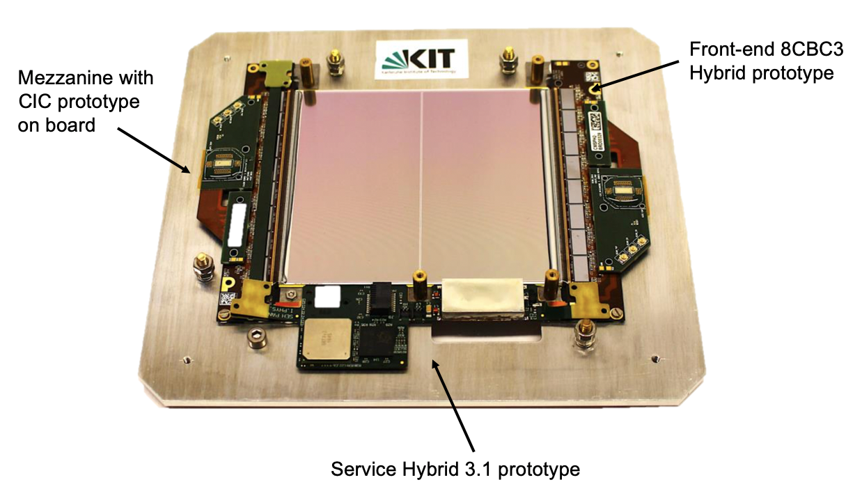
Both pT modules have two different types of high density interconnect hybrid circuits which house the front-end and auxiliary electronics. The hybrids are stand-alone units that are connected via bidirectional optical links to the backend electronics with no intermediary aggregator system. The front-end hybrids host the readout chips and the concentrator chip while the service hybrids house the opto-electronics and the DC-DC converters for powering. Each side of the module is connected to a front-end hybrid. For both module types the signals from the top and bottom sensor are routed to one readout chip to perform the track stub finding. This is achieved by using a flexible hybrid which is folded over a spacer and which allows routing of the signal between the different parts of the module. A sketch of both module types with their front-end and other hybrids is shown in the Fig. 6.
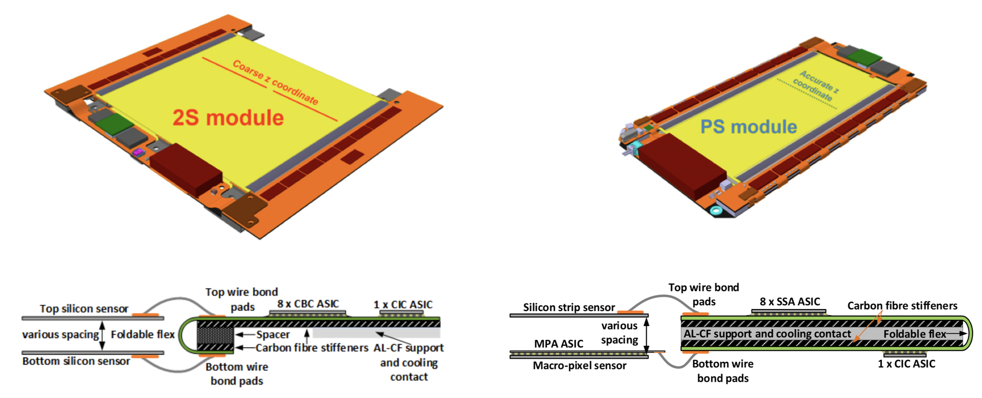
The 2S module features two silicon strip sensors each with two columns of 1016 strips with single strip size of 5 cm 90 m. Each sensor side is read out by eight readout chips (CBC) implemented in 130 nm CMOS technology. A CBC chip reads 254 strips (127 from bottom and 127 from top sensor strips), performs hit correlation between the two sensors and sends the stub data out at each bunch crossing to the concentrator chip (CIC, designed in 65 nm CMOS technology), that performs data sparsification, formats the output data, and sends them to the service hybrid. The service hybrid hosts the LpGBT, VTRx+ optical link, DC-DC converters and HV distribution circuitry. The data from the front-end hybrids are merged and sent via a single optical fibre to the back-end electronic system.
The PS module is made of one silicon micro-strip sensor with two columns of 960 strips each with single strip size of 2.5 cm 100 m, and a macro-pixel sensor with a matrix of 32 960 pixels with a pixel size of 1.5 mm 100 m. The strip sensor is read out by two times eight short strip ASIC (SSA), while the macro-pixel sensor is read out by sixteen macro pixel ASIC (MPA); both chips are implemented in 65 nm CMOS technology. The track stub finding in the PS modules is done by the MPA. The MPA chip receives the information about strip clusters from the SSA which sends them together with information about the bunch crossing in which a hit occurred. The MPA combines this information with the macro-pixel information to form track stubs. The transfer scheme and data formats are very similar to those used in the 2S module, allowing the same CIC chip to be used for performing the same data collection, sparsification and formatting functions as for the 2S module. For space reasons, the PS module has two service hybrids, one for the optical system and one for the powering.
The module design uses novel composite materials (Al-CF) and all structural components have been chosen for their high thermal conductivity, low CTE, and minimal material budget.
4 Material budget and performance
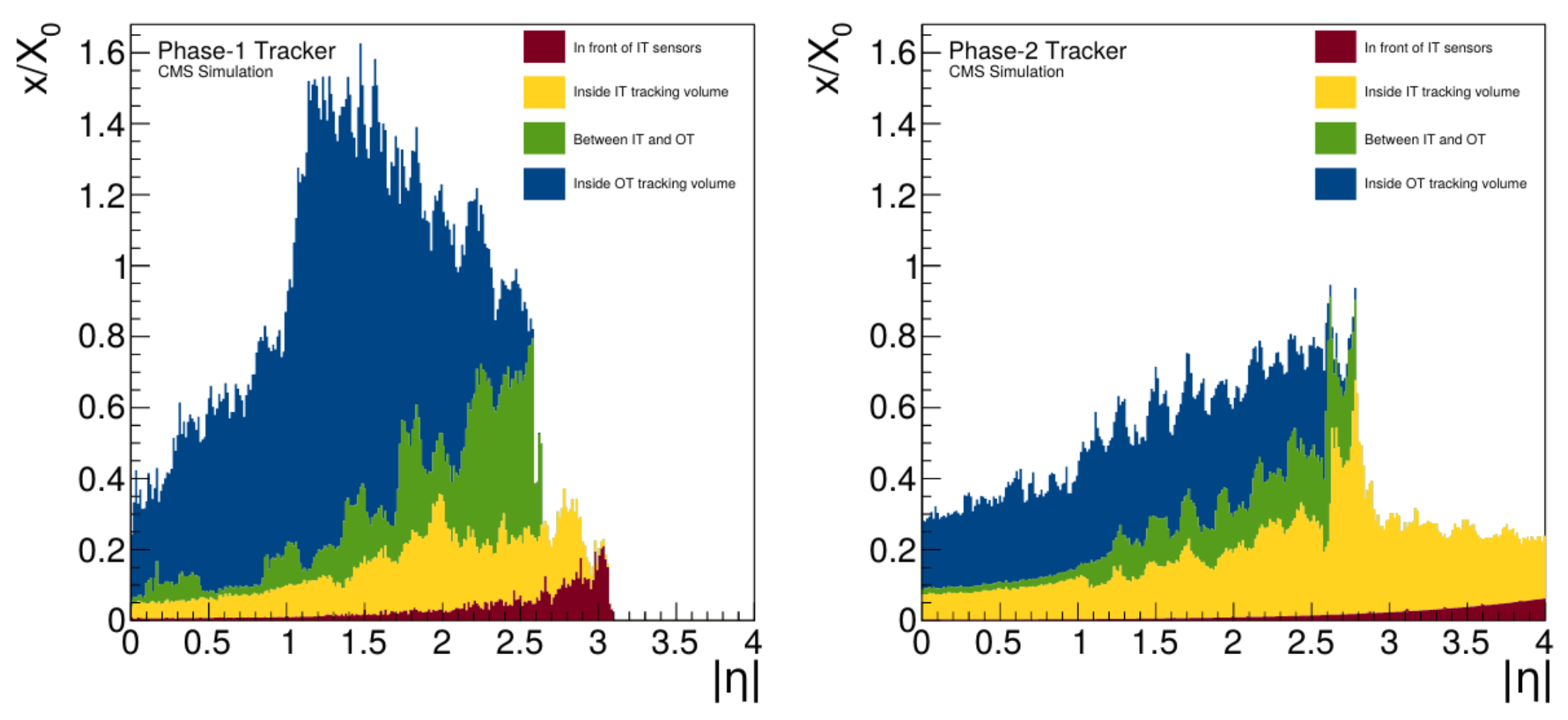
Despite the increased number of readout channels in the new tracker the estimated material budget shows a significant reduction compared to the currently installed tracker as is shown in Fig. 8. The key features to achieve this reduction are: a reduced number of layers, an optimised routing of the services, use of light weight material, low-mass CO2 cooling as well as the use of DC-DC converters (OT) and serial powering (IT).
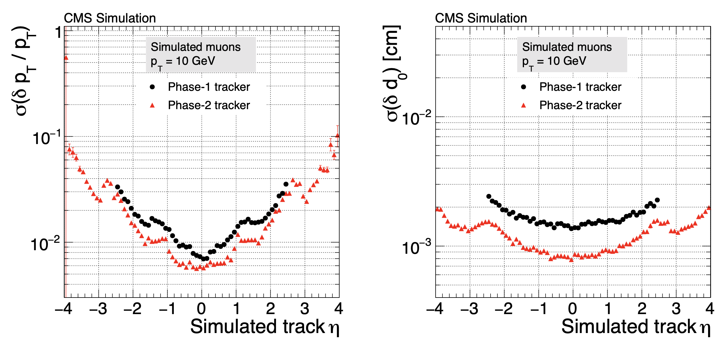
Also the tracking and vertexing capabilities of the new tracker will be better than for its predecessor. Figure 9 shows the pT resolution (left) and impact parameter resolution (right) comparison between the currently installed tracker (Phase-1) vs. the new tracker (Phase-2), respectively.
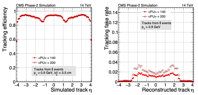
As shown in Fig. 10, the new tracker is also expected to be capable of maintaining a high tracking efficiency (about 90%) at the high pile-up and have a fake rate below few percent.
5 Summary
The CMS Phase-2 Tracker is an ambitious project that has to cope with a higher pile-up and radiation environment at the HL-LHC. The new tracker will consist of about 200 m2 of silicon and will be made up of the Outer Tracker using modules containing pairs of closely spaced sensors, and the Inner Tracker with silicon pixel sensors. The key features of the new tracker are the high granularity, radiation hardness, low material budget and the capability to provide tracking information to the first stage of the CMS trigger system. The project is overall in good shape and on-track for installation in LS 3 with the Inner Tracker entering the prototyping phase and the Outer Tracker in prototyping phase with first items entering the pre-production phase.
References
- [1] G. Apollinari et al., High-Luminosity Large Hadron Collider (HL-LHC), CERN Yellow Rep. Monogr. 4 (2017) 1-516 [https://cds.cern.ch/record/2284929].
- [2] ATLAS Collaboration, The ATLAS Experiment at the CERN Large Hadron Collider, JINST 3 (2008) S08003 [https://cds.cern.ch/record/1129811].
- [3] CMS Collaboration, The CMS Experiment at the CERN LHC, JINST 3 (2008) S08004 [https://cds.cern.ch/record/1129810].
- [4] CMS Collaboration, The Phase-2 Upgrade of the CMS Tracker - Technical Design Report, CERN-LHCC-2017-009, CMS-TDR-014 [https://cds.cern.ch/record/2272264].
- [5] J. Christiansen et al., R&D collaboration proposal: Development of pixel readout integrated circuits for extreme rate and radiation, Technical report CERN-LHCC-2013-008, LHCC-P-006, CERN [https://cds.cern.ch/record/1553467].
- [6] RD53 Collaboration, The RD53A Integrated Circuit, Technical report CERN-RD53-PUB-17-001, 2017 [https://cds.cern.ch/record/2287593].
- [7] T. Heim, First test results from the ITkPixV1 pixel readout chip, presented at VERTEX 2020 conference, this proceeding.
- [8] B. Ristic, Prototype Module Construction for the High Luminosity Upgrade of the CMS Pixel Detector, PoS Vertex-19 (2019) 058 [http://cds.cern.ch/record/2720556].
- [9] S. Kulis, The lpGBT design, status and plan, presented at ACES 2018 - Sixth Common ATLAS CMS Electronics Workshop for LHC Upgrades, CERN, April, 2018 [https://indico.cern.ch/event/681247/contributions/2928992].
- [10] J.Troska et al. The VTRx+, an optical link module for data transmission at HL-LHC, PoS TWEPP-17 (2017) 048 [https://cds.cern.ch/record/2312396].
- [11] W. Adam, et al., Beam test performance of prototype silicon detectors for the Outer Tracker for the Phase-2 Upgrade of CMS, J. Inst. 15, IOP Publishing, (2020) P03014 [http://cds.cern.ch/record/2715750].
- [12] W. Adam, et al., Experimental study of different silicon sensor options for the upgrade of the CMS Outer Tracker, J. Inst. 15, IOP Publishing, (2020) P04017 [https://cds.cern.ch/record/2706001].
- [13] G. Saha, Performance of the 2S Modules of the CMS Phase 2 Tracker in a Test Beam environment, presented at VERTEX 2020 conference, this proceeding.