cdspata@sandia.gov
Nanoscale functionalized superconducting transport channels as photon detectors
Abstract
Single-photon detectors have typically consisted of macroscopic materials where both the photon absorption and transduction to an electrical signal happen. Newly proposed designs suggest that large arrays of nanoscale detectors could provide improved performance in addition to decoupling the absorption and transduction processes. Here we study the properties of such a detector consisting of a nanoscale superconducting (SC) transport channel functionalized by a photon absorber. We explore two detection mechanisms based on photo-induced electrostatic gating and magnetic effects. To this end we model the narrow channel as a one-dimensional atomic chain and use a self-consistent Keldysh-Nambu Green’s function formalism to describe non-equilibrium effects and SC phenomena. We consider cases where the photon creates electrostatic and magnetic changes in the absorber, as well as devices with strong and weak coupling to the metal leads. Our results indicate that the most promising case is when the SC channel is weakly coupled to the leads and in the presence of a background magnetic field, where photo-excitation of a magnetic molecule can trigger a SC-to-normal transition in the channel that leads to a change in the device current several times larger than in the case of a normal-phase channel device.
I Introduction
The most efficient single-photon detectors are currently based on superconducting (SC) nanowires Goltsman ; Natarajan ; Karl . A single-photon absorption event in the superconductor is followed by a sequence of relaxation processes involving electron-electron and electron-phonon interactions, which culminate in the creation of a hot spot that triggers a phase transition to the normal state Allmarass . Bypassing the energy cascade associated with such photo-induced temperature effects is desirable because it reduces the time scale for detection and the associated jitter. Besides temperature, there are other effects that directly impact the SC state such as electro-strictive, electrostatic gating and magnetic interactions. The question we seek to answer is whether such effects can be exploited for single-photon detection.
In parallel, there has been interest in developing new detector architectures that can overcome the limitations of existing systems. Along those lines, it was recently proposed that dense arrays of nanoscale detector elements could provide significant performance improvements Young . One embodiment of such detector elements consists of functionalization nanoscale electronic transport channels functionalized with molecules, quantum dots, or other photon absorbers Leonard_SciRep ; Bergemann . We recently studied the detailed quantum dynamics of single-photon detection in a functionalized semiconducting electronic transport channel Spataru_singlePh and found that a large signal-to-noise-ratio can be achieved for ultra-short single-photon pulses. An open questions is whether a SC electronic transport channel could be more efficient at detecting single photons, allowing to also bypass the thermal energy cascade.
Here we combine the Keldysh non-quilibrium Green’s function formalism Keldysh with the Nambu description Nambu of the superconductor to study the change in electronic transport through a SC channel upon absorption of a photon by a nearby absorber. We consider the cases where the absorber undergoes changes in its permanent electric dipole or magnetic moment. In both cases the direct electromagnetic interaction between the absorber and the SC channel bypasses the usual thermal energy cascade. We show that under certain conditions photo-induced magnetic perturbations can trigger a SC-to-normal transition in the channel which in turn leads to a detectable event.
II Device system
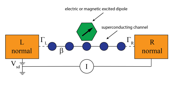
We consider a normal-superconductor-normal (NSN) device configuration with the device geometry sketched in Fig. 1. It consists of a SC one-dimensional channel contacted by two normal metal electrodes. In practice the channel could be a nanowire or a nanotube CNT_SC ; WS2_NT which have been shown to have SC transition temperatures in the 5-15K range, but to reduce computational cost while capturing essential physics, here we model it as an atomic chain within the tight-binding approximation. We focus on a single band since the second subband is typically much higher in energy than the SC gaps considered here. As opposed to typical SC nanowire single-photon detectors, photon absorption does not take place in the channel but by an absorber placed in close proximity to the SC channel.
We assume that the photon energy is resonant with the absorber while the channel is not sensitive to the incoming light pulse (e.g., a small-diameter CNT has well-separated optical absorption peaks due to excitonic effects; we assume that the absorber optical gap is not matched to these peaks. We also assume that the system operates in the strong focusing regime where the light is concentrated on the absorbing element. This increases the light-absorber interaction and also helps to reduce the effects from absorption by the contacts. The absorber (represented in Fig. 1 by the hexagon) could be a single-molecule or a larger quantum-dot that upon photo-excitation acquires a permanent electric or magnetic dipole, possibly via a photo-induced phase transition NewRef . In the present work we do not calculate the absorber photoexcitation probability; rather we assume that the absorber has been photoexcited and we calculate the impact of the excited dipole on the electronic transport properties of the channel.
As possible detection mechanisms we consider either i) photo-induced electrostatic gating effects -e.g. due to a change of the absorber permanent electric dipole upon photo-excitation, or ii) photo-induced magnetic effects -e.g. due to a change in the absorber magnetic moment upon photo-excitation. Both types of perturbation can change the electronic density of states (DOS) at the Fermi level when the channel is in the normal phase and thus are expected to affect the SC state as well. In particular it has been discovered that monolayers of paramagnetic molecules can influence the temperature at which an adjacent thin layer of material becomes SC magM1 ; magM2 ; magM3 . In addition, photon-induced changes in molecular magnetic moments have been observed MM_ph . Changes in molecular electric dipole moments are well-known to occur upon photon absorption, and have been shown to modulate semiconducting electronic transport channels Leonard_SciRep . Their impact on SC channels may be expected based on the report of SC transistors where the gate is essentially equivalent to an electrostatic dipole SC_transistor .
III Theoretical framework
III.1 Tight-binding Hamiltonian
The device is described within the grand-canonical picture using a Hamiltonian partitioned into left () and right () leads and channel () regions:
| (1) |
where are the electron number operators in the left (L) and right (R) regions while the difference between left and right lead chemical potentials defines the applied bias.
The channel Hamiltonian is described using a tight-binding basis set with indices :
| (2) |
The first term describes the bare channel with no electron interaction effects, with the nearest neighbor hopping integral set to eV and an inter-site distance set to bohr (the summation over is restricted to ). The number of sites in the transport channel is denoted by .
The second, Hubbard-like local term includes electron correlation effects via an attractive contact interaction corresponding to a s-wave type SC pairing potential. Here is the local number operator for an electron with spin that can be either up () or down (). We do not consider Coulomb interaction/electron correlation effects in the channel when the channel is in the normal state. The impact of repulsive Coulomb interaction effects could be important in certain device parameter regimes where exotic effects such as the Kondo effect may become important Hewson ; Wang ; SpataruKondo . Including these effects is however beyond the scope of the present work.
The third term describes an applied gate voltage acting uniformly along the channel. Magnetic effects are included via the last term which removes local spin-degeneracy via the Zeeman effect and accounts for: i) a uniform background magnetic field perpendicular to the chain, and ii) a non-uniform magnetic field generated by an excited absorber with a permanent magnetic dipole perpendicular to the chain.
Finally, the coupling between leads and channel is assumed L-R symmetric and characterized by the induced broadenings . The SC pairing potential is zero inside the leads.
III.2 NEGF approach
To describe non-equilibrium effects in conjunction with SC phenomena we employ the Keldysh-Nambu non-equilibrium Green’s function (NEGF) formalism (see the Appendix for details including the definition of the 4-component Nambu spinors.). NEGF-based studies of non-equilibrium phenomena in NSN junctions have employed both self-consistent Lambert ; Yeyati1 ; Yeyati2 and non-self-consistent Claro ; Tuovinen1 ; Tuovinen2 approaches. Here ’self-consistent’ refers to the determination of the order parameter . In this work is calculated rigorously via a self-consistent approach, directly from the off-diagonal Nambu component of the lesser Green’s function: . The self-consistent process starts with a symmetry-broken initial guess e.g. by setting the order parameter to a constant. Convergence is facilitated by the use of the Pulay scheme Pulay to mix the order parameter using previous iterations solutions Spataru_AM1 . Convergence is typically achieved in hundred iterations when .
We present briefly the NEGF expression for the expectation value of the current through the device (see the Appendix for derivation). The current can be decomposed into the normal transmission/single-electron tunneling (), Andreev reflection () and cross-Andreev () components Andreev ; Blonder ; Devoret ; Falci ; CAR_L of the current: . For the device parameters considered in this work the cross-Andreev component is negligible and it is sufficient to focus on the first two components, namely normal transmission Wingreen
| (3) |
and Andreev reflection Andreev
| (4) |
where is the Fermi-Dirac distribution function and refers to the component (in Nambu space) of the retarded/advanced channel Green’s functions. The diagonal Nambu component is also used to obtain the electronic density of states projected on the channel:
| (5) |
We note that the chemical potentials are referenced w.r.t. the chemical potential of the SC condensate . While in general in the presence of superconductivity () needs to be determined self-consistently by imposing current conservation Lambert along the channel, for the particular case where the total system has electron-hole symmetry is simply equal to the middle of the electronic band of either lead, i.e. it can be set to .
In our simulations we consider devices where the channel is SC () and undergoes a transition to a normal state as well as channels that are always in the normal state (). We label the currents with the superscripts SC and N to denote these two cases. As above, subscripts are reserved for the components of the current when the channel is subject to superconductivity.
IV Results
IV.1 Good metal contacts/strong channel-electrodes coupling
First we consider the case of good metal contacts between source/drain electrodes and the transport channel. This is established by setting the coupling between leads and channel of the same order of magnitude as the hopping parameter inside the channel , and as a representative value we choose . We consider a channel with and tune the gate voltage such that at zero source-drain bias voltage the Fermi level pins the middle of the channel electronic band (which has a bandwidth of eV). In the normal (N) phase, the DOS is flat near the Fermi level, with small oscillations due to the fact that the energy spectrum is discrete. Upon turning on the attractive contact interaction term eV, the channel becomes SC and a quasiparticle gap opens up in the DOS near the Fermi level, as seen in Fig. 2(a). The finite value of DOS near the Fermi level is due to the contribution from sites near the normal metal contacts. The channel is long enough that towards the middle of the channel the gap opening is nearly perfect. We note that at zero temperature and zero bias voltage the SC gap is about meV; while this leads to a relatively large critical temperature -as discussed later-, it also helps in reducing the number of iterations needed to reach convergence - each iteration during the self-consistent loop is computationally demanding given the large .
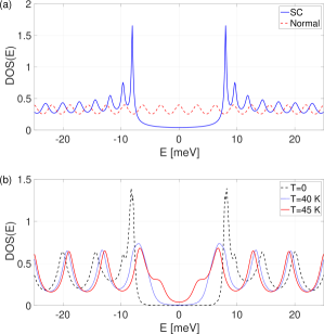
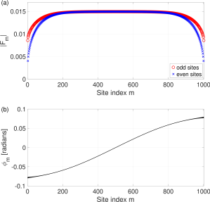
Figure 3 shows the channel SC order parameter at and small bias voltage meV. is not impacted significantly by the small bias voltage, but is sensitive to the proximity of the normal-phase contacts and thus decreases in value near the ends of the channel. One notes in Fig. 3(a) that is asymmetric between even and odd sites. This can be traced back to the normal phase where electron wavefunctions associated with eigenchannels with energies near the middle of the channel electron band show strong asymmetry; in particular the eigen-channel with zero energy carries its entire weight on the odd sites. Figure 3(b) shows the phase which displays a gradient that increases with the bias voltage/current. Within more approximate theories where is assumed to be a constant independent of , the phase gradient is directly related to the momentum of the Cooper pairs: . A non-zero simply corresponds to the flow of the SC condensate which carries a finite current when a bias voltage is applied.
The SC gap parameter is directly related to the magnitude of the gap seen in Fig. 2 in the electronic DOS of the SC phase, i.e. . The dependence of on shows the expected BCS BCS behavior as seen in Fig. 4(a). In the limit of small bias voltage the channel is in the normal phase for temperatures above the critical temperature K. At the SC gap parameter has a value of meV which yields a ratio . This is slightly smaller than the BCS ratio of due to being smaller near the normal metal contacts than in the middle of the channel (as seen in Fig. 3(a)). One can also estimate the SC coherence length according to BCS theory as , implying that the average comprises about sites, which correlates well with the length scale over which the order parameter decreases exponentially towards the contacts as seen in Fig. 3(a).
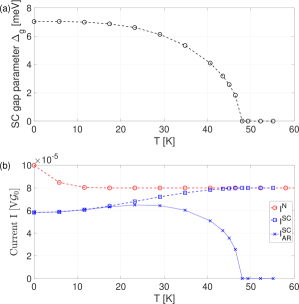
Figure 4(b) shows the dependence of the expectation value of the current through the device , calculated for a fixed low bias voltage meV. In the normal phase, the zero-temperature, zero-bias conductance equals the quantum unit of conductance , with electrons tunneling resonantly through the channel mid-bandwidth level irrespective of the contact transmissivity/coupling parameter . As increases, the energy window through which electrons tunnel increases; for K, the effective DOS contributing to the current gets averaged over several energy levels that are broadened by the coupling to the leads. For , the resulting averaged DOS is of the peak DOS (Fig. 2), explaining the decrease in current seen in Fig. 4(b). Turning to the SC case, one notes that the current/conductance is smaller than in the normal case. This is due to the non-ideality of the metal contacts. Indeed, for a NSN device at zero-temperature, the zero-bias SC conductance approaches (i.e. , the conductance of each NS interface approaches ) only if the electron transmission probability between the contacts and the normal-phase channel approaches unity in a finite window around the Fermi level Cuevas1 ; Klapwijk ; Sun1 ; WPan . Within the wide-band limit (WBL) approximation for the leads this happens when . For our less ideal choice , one finds at that the conductance is about . As seen in 4b, at the SC current takes place via Andreev reflection (AR), as the normal current component is suppressed given the near perfect DOS gap opening in the bulk of the channel (the cross-Andreev component is negligible due to the large channel length). As the temperature increases the DOS gap gets smaller and the DOS at becomes finite even when projected towards the middle of the chain, as seen in Fig. 2(b). Correspondently the normal component increases until it completely dominates the current for .
We note from Fig. 4(b) that the continuous decrease of as approaches results in smoothly approaching with no apparent discontinuity in the current or in its derivative . Ideally, we would like a device based on a SC channel to switch between the SC and normal state upon photo-excitation, accompanied by a detectable change in the measured current. For relatively small perturbations such us those expected to be induced by a single-photon absorption event, an appreciable change in the current could be obtained if the transition is accompanied by a discontinuous change in the current. Unfortunately, for this device configuration the current undergoes a smooth transition as changes from below to above as seen in Fig. 4(b), suggesting that the device may not offer a significant advantage over its normal-phase-only counterpart.
Because in this work we do not consider phonon-based temperature effects that may assist single-photon detection, we focus our attention on the behavior of the device as function of bias voltage. Figure 5 shows the characteristic of a device with a smaller channel (we consider to reduce the computational effort), driven beyond the critical voltage/current while the leads are maintained at . In the absence of SC the current shows almost linear dependence on the bias voltage , i.e. a behavior close to Ohmic - as expected given the good metal contacts. For low the SC current is about lower than in the normal-phase, and it approaches at the critical voltage mV. Translated into temperature, yields a value larger than the critical temperature K. We note that the Andreev reflection of the current drops rather smoothly to zero at ; as a consequence the I-V characteristics does not show any discontinuity near the critical voltage. We conclude that for the configurations considered in this section, where the channel is coupled strongly to the electrodes, it is unlikely for the device to undergo a significant change in current due to a small photo-induced perturbation and that a different design strategy is needed.
IV.2 Poor metal contacts/weak channel-electrodes coupling
A previous study Snyman used quasiclassical Green’s functions to show that the I-V characteristics of NSN structures displays, in certain regions of the device parameter space, a discontinuity as the voltage is swept. The behavior of our device as a function of bias voltage suggests this not to be the case when the channel is strongly coupled to the electrodes. Thus, in this section we consider the opposite case of weak coupling between channel and electrodes obtainable by setting . In practice, weak channel-electrodes coupling can be realized using few-nm thin insulating materials inserted between the electrode and the channel.
We are interested in a situation Snyman where in the absence of SC only one channel level contributes to electronic transport for small bias voltage. This can be obtained e.g. by setting , meV which yields a separation between channel levels near the Fermi level meV significantly larger than the level broadening . Figure 6 shows the DOS of such a device in a small energy window near the Fermi level. In the absence of SC, the wavefunction associated with the zero-energy channel level carries its entire weight on the odd sites. We also set meV such that the resulting SC gap opening in the DOS meV is larger than the level broadening but significantly smaller than .
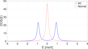
Figure 7 shows the channel SC order parameter at . We note that the weight of on odd sites is more than an order of magnitude larger than the one on even sites. It is important to note that capturing this feature is not possible without obtaining the SC order parameter self-consistently. Averaging over all the sites and multiplying by leads to a SC gap parameter meV, while averaging only over the odd sites (those that carry the weight of the zero-energy eigen-channel in the absence of SC) one obtains meV. The latter parameter can be related to the gap opening in the DOS via the usual relationship: .
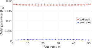
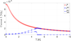
Figure 8 shows the dependence of the current through the device , calculated for a fixed low bias voltage meV. As discussed previously, in the normal phase, the zero-temperature, zero-bias conductance equals . A bias voltage meV is significant enough (w.r.t. the broadening of the central energy level) to decrease the normal-phase zero-temperature conductance value to . Increasing temperature also reduces the normal-phase conductance, this time much more significantly than seen in Fig. 4(b). Turning to the SC case, we note two differences w.r.t. to the case depicted in Fig. 4(b). First, at , the poor electron transmission between leads and channel results in a conductance more than smaller than . This can be explained by the fact that the effective broadening of the relevant channel electronic level meV (estimated from the HWHM of the central peak in Fig. 7) is significantly smaller than the effective gap parameter meV. Indeed, projecting Eq. (4) in the subspace of the only relevant electronic eigen-channel, the zero-bias Andreev reflection conductance reads (see also Eqs. (A-24), (A-27) and (A-28)):
| (6) |
which yields . Second, as the temperature approaches K, while the SC current approaches continuously its normal counterpart , its derivative displays a discontinuity at due to the sudden drop of the Andreev reflection component of the current . This discontinuity suggests that the I-V characteristics of the device with poor metal contacts may be fundamentally different than in the good metal contacts case and perhaps it may show more sensitivity to photo-induced perturbations.
IV.2.1 Impact of small electrostatic gating and magnetic perturbations
We consider two mechanisms that can lead to photodetection: i) a change in the absorber permanent electric dipole moment Spataru_singlePh ; Leonard_SciRep , e.g. as in functionalization with chromophores. This electric dipole change generates an electrostatic potential that acts as a gating potential for the channel. For simplicity we mimic this situation with a uniform gating electrostatic potential as the prototype electrostatic perturbation, but we have checked that non-uniform potentials non-unif_pot lead to similar conclusions. ii) a change in the absorber’s permanent magnetic dipole moment , e.g. as in functionalization with small magnetic molecules. We also use a uniform magnetic field to perform an initial assessment of the impact of magnetic perturbations.
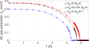
We start our analysis by studying the behavior of the SC gap parameter as function of temperature, as shown in Fig. 9. In the absence of an electrostatic gating or magnetic perturbation, shows a similar behavior as in the case of good metal contacts (compare to Fig. 4). Adding a relatively small electrostatic gating potential mV yields a reduction in both and , while a uniform magnetic field T reduces by a fraction of a Kelvin but has negligible impact on . The reduction of may be explained by the fact that in the normal phase both types of perturbation result in a decrease of the DOS at the Fermi level.
Based on the above results one could expect that an electrostatic gating potential has a greater impact on the I-V device characteristics than a magnetic field. As discussed next, the results shown in Fig. 10 indicate that this is not the case. First, in the absence of any external perturbation, as seen in Figs 10(a) and 10(b), the normal-phase current shows non-linear behavior due to the non-Ohmic character of the metal contacts. In fact develops a plateau when increases beyond the resonant-level broadening. Turning to the SC case, an important feature is that the current undergoes a sharp jump near the critical voltage mV. The jump is significant, amounting to .
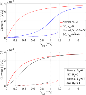
Figure 10(a) shows the impact of the electrostatic gating potential mV on the I-V characteristics. Because the channel level through which electrons tunnel is off-resonance, the normal-phase current is much reduced w.r.t. the case at . As increases beyond both the level broadening and , starts approaching the unperturbed values. We find that as long as the channel is in the SC phase, for , the electrostatic gating potential has no impact on the current or the critical voltage . This is a somewhat unexpected finding given that mV does have an appreciable impact on as seen in Fig. 9. While all the results in Fig. 10 are obtained with metal contacts maintained at , we have tried other temperatures but always reached the same result, namely that the electrostatic gating mechanism is not effective at improving the light-detection efficiency of a functionalized SC channel w.r.t. it normal-phase counterpart.
The impact of a uniform magnetic field surf_currents T is seen in Fig. 10(b). In the normal phase, its effect is to reduce the current by a factor of at and by about at mV. In the SC case, the reduction of is for mV. Interestingly, the impact of increases at higher and most importantly it results in an decrease of the critical voltage from mV to mV. This suggests that functionalizing a SC with a magnetic molecule might result in an efficient detector if one operates the device near and if the photo-excitation of the molecule induces a local magnetic dipole whose associated magnetic field is strong enough to yield a measurable change in .
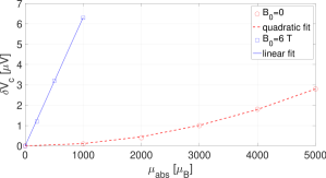
To estimate the impact of a photo-excited magnetic absorber on the critical voltage we consider a magnetic dipole characterized by a magnetic moment and positioned at a distance nm away from the central atom of the SC channel. The magnetic dipole is oriented perpendicular to the plane defined by the channel and the line joining the magnetic dipole and the mid-channel site. The magnetic potential field at the channel site ’m’ situated at a distance from the mid-channel site is with the vacuum permeability, and the corresponding Zeeman splitting potential acting on spin up/down electrons in the chain is spin_suscep .
We calculate the I-V characteristics in the vicinity of for various and extract the change , as plotted in Fig. 11 with red circles. As expected from the symmetry of the problem w.r.t. a change in sign of the magnetic field, we find that depends quadratically on : , as indicated by the quadratic fit plotted with the red, dashed line. Quantitatively, the change is on the order of V for of about . This large change in may be difficult to achieve for single photon absorption.
However, the quadratic behavior also implies that the presence of a background magnetic field significantly larger than the one produced by can amplify the impact of an added magnetic moment: . Indeed, Fig. 11 shows that in the presence of a background uniform magnetic field T, the change shows a linear dependence on with a slope of . Translated into temperature, one obtains that a change mK can be obtained by an excited absorber magnetic moment .
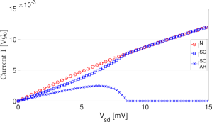
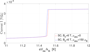
Figure 12 shows the I-V characteristics of the device in the presence of a background uniform magnetic field T. We consider a magnetic molecule that has no magnetic dipole in the ground state but carries a magnetic moment in the excited state. As noted previously, the change in the critical voltage is about mK upon photo-excitation of the magnetic molecule. Controlling the voltage within mK is experimentally feasible, which means that if one operates the device while maintaining the bias voltage within mK below the critical voltage, photoexcitation of the magnetic molecule would trigger the SC-to-normal phase transition of the channel. As seen in Fig. 12, this transition is accompanied by an increase of the current by a factor , i.e. orders of magnitude higher than one would obtain with a normal-phase channel and otherwise similar device parameters. For comparison, we found that the current through a semiconducting but otherwise similar electronic transport channel may increase, due to a photo-induced Debye electrical dipole situated about nm away from the channel, by a factor of at most upon device optimization Spataru_singlePh .
IV.3 Conclusion
We have studied a photon detector device that consists of a functionalized SC transport channel contacted by two normal-phase metal electrodes. We have considered two possible detection mechanisms based on i) electrostatic gating effects (e.g. functionalization with chromophores) and ii) magnetic effects (e.g. functionalization with magnetic molecules). We found that optimal device designs require weak coupling between the leads and the channel (e.g. using insulating layers to separate the metal contacts from the channel) such that only one channel electronic level participates in transport and the I-V device characteristics shows a discontinuity near the critical voltage. Our results indicate that the electrostatic gating mechanism is not effective for triggering a SC-to-normal transition. However, we find that magnetic effects offer an efficient photo-detection mechanism whereas in the presence of a background magnetic field, photo-excitation of a magnetic molecule may trigger a SC-to-normal transition accompanied by a measurable change in the device current.
Appendix: Self-consistent Keldysh-Nambu NEGF formalism
To account for superconductivity and non-equilibrium phenomena the relevant Keldysh Green’s function is defined using -component Nambu spinors:
| (A-1) |
where denotes time ordering along the double-time Keldysh contour.
For BCS-type superconductivity with coupling between opposite spins and in the presence of either spin or electron-hole symmetry (which are the situations considered in this work), we may use only 2-component Nambu spinors. Neglecting for the sake of simplicity spin indices (the spin structure is ,,, for the 11,12,21,22 Nambu components respectively), the Keldysh Green’s function is written in the reduced Nambu space:
| (A-2) |
The corresponding Keldysh components lesser (), greater (), advanced (), and retarded () of the Green’s function are then:
| (A-3) |
| (A-4) |
| (A-5) |
| (A-6) |
If we reference all single-particle energies as well as the lead chemical potentials w.r.t. the condensate chemical potential when superconductivity is present, then at steady-state one can replace the double-time dependencies with the time difference . After Fourier-transform we obtain:
| (A-7) |
| (A-8) |
and similar for the other Keldysh components. Note that [or ] so one can write (T stands for transpose):
| (A-9) |
and
| (A-10) |
To calculate the Green’s functions we approximate self-energies at the Hartree-Fock level.
The non-interacting, isolated channel Green’s function is:
| (A-11) |
Here we used that is symmetric because the channel Hamiltonian is symmetric with real matrix elements and real eigenvectors . Then .
In the channel eigenstate basis (indexed by ), one has:
| (A-12) |
and
| (A-13) |
The non-interacting, isolated leads Green’s functions, are written in the leads eigenstate basis (indexed by ) as:
| (A-14) |
where:
| (A-15) |
and
| (A-16) |
Also,
| (A-17) |
with:
| (A-18) |
and
| (A-19) |
where is the Fermi-Dirac distribution function and we used that . We emphasize that all single-particle energies as well as the chemical potentials of the leads must be referenced w.r.t. the chemical potential of the SC condensate in order for the above expressions to be valid when superconductivity is present. can be determined self-consistently by imposing current conservation Lambert along the channel. For the case where the total system has electron-hole symmetry one has .
The leads are treated within WBL in which case the retarded lead self-energies are purely imaginary:
| (A-20) |
where ( is the leads-channel tunneling Hamiltonian):
| (A-21) |
while the lesser lead self-energies are:
| (A-22) |
The channel Green’s functions are obtained via the equations:
| (A-23) |
| (A-24) |
and
| (A-25) |
The SC pairing potential inside the channel has the form: ( are the Pauli matrices). This interaction has zero contribution to the Hartree self-energy diagram while the channel Fock self-energy is obtained self-consistently via:
| (A-26) |
where stands for element-by-element multiplication in Nambu space. We note that the integral vanishes as it is equal to which is zero by virtue of equal-time fermion anti-commutation rules.
For the SC pairing potential one chooses an attractive, contact interaction (see the Hubbard-like term of in eq. (2)) which leads to:
| (A-27) |
The SC gap parameter is defined as times the average of the SC order parameter over the channel sites:
| (A-28) |
IV.1 Current expression
To obtain the expression for the current one starts from the usual expression Wingreen ; Spataru_AM1 ; Claro for the current through the left contact
| (A-29) |
where stands for the upper diagonal Nambu component. In the last equality we made use of Eqs. (A-22)-(A-24).
Further use of Eq. (A-23) as well as permutation properties of symmetric matrices (inside the trace) yields:
| (A-30) |
where the normal transmission (NT) component is:
| (A-31) |
and the Andreev reflection (AR) / cross-Andreev (CA) components read:
| (A-32) |
| (A-33) |
with being the Nambu component of the retarded/advanced Green’s functions. We note that the cross-Andreev component of the current vanishes in the case where the lead chemical potentials are symmetric w.r.t. SC condensate chemical potential (i.e. ).
A similar expression holds for the current through the right contact (for the steady-state situations considered in this paper one has ).
The expressions for the current can be evaluated numerically as simple matrix multiplications, taking advantage of the fact that the integrals over can be reduced to the form [ being the complex eigenvalues of ]:
| (A-34) |
which is evaluated analytically by performing the exact summation -using the digamma function- over the residues of the Fermi-Dirac distribution function .
Acknowledgements.
Work supported by the Defense Advanced Research Projects Agency (DARPA) DETECT program. The views, opinions and/or findings expressed are those of the author and should not be interpreted as representing the official views or policies of the Department of Defense or the U.S. Government. Sandia National Laboratories is a multi-mission laboratory managed and operated by National Technology and Engineering Solutions of Sandia, LLC., a wholly owned subsidiary of Honeywell International, Inc., for the U.S. Department of Energy’s National Nuclear Security Administration under contract DE-NA-0003525.References
- (1) G. N. Gol’tsman, O. Okunev, G. Chulkova, A. Lipatov, A. Semenov, K. Smirnov, B. Voronov, A. Dzardanov, C. Williams, and R. Sobolewskib, Appl. Phys. Lett. 79, 705 (2001).
- (2) C.M. Natarajan et al., Supercond. Sci. Technol. 25, 063001 (2012).
- (3) F. Marsili, F. Bellei, F. Najafi, A.E. Dane, E.A. Dauler, R.J. Molnar, K.K. Berggren, Nano. Lett. 25, 4799 (2012).
- (4) J.P. Allmaras, A.G. Kozorezov, B.A. Korzh, K.K. Berggren, and M.D. Shaw, Phys. Rev. Appl., 11, 034062, (2019).
- (5) S.M. Young, M. Sarovar, F. Léonard. ACS Photonics, 7, 821 (2020).
- (6) K. Bergemann, F. Léonard. Small, 14, 1802806 (2018).
- (7) F.Léonard, M.E. Foster, and C.D. Spataru, Sci. Reports 9, 3268 (2019).
- (8) C. D. Spataru and F. Léonard, Phys. Rev. Res. 1, 013018 (2019).
- (9) L. V. Keldysh, Zh. Eksp. Teor. Fiz. 47, 1515 (1965) [Sov. Phys.–JETP 20, 1018 (1965)].
- (10) Y. Nambu, Phys. Rev. 117, 648 (1960).
- (11) K. Tang, L. Zhang, N. Wang, X. X. Zhang, G. H. Wen, G. D. Li, J. N. Wang, C. T. Chan, P. Sheng, Science 292, 2462 (2001).
- (12) F. Qin, W. Shi, T. Ideue, M. Yoshida, A. Zak, R. Tenne, T. Kikitsu, D. Inoue, D. Hashizume, and Y. Iwasa, Nat. Commun. 8, 14465 (2017).
- (13) E. Macchia, K. Manoli, B. Holzer, C. Di Franco, M. Ghittorelli, F. Torricelli, D. Alberga, G.F. Mangiatordi, G. Palazzo, G. Scamarcio, L. Torsi, Nat. Comm. 9, 3223 (2018).
- (14) G. Serrano, L. Poggini, M. Briganti, A.L. Sorrentino, G. Cucinotta, L. Malavolti, B. Cortigiani, E. Otero, P.Sainctavit, S. Loth, F. Parenti, A.-L. Barra, A. Vindigni, A. Cornia, F. Totti, M. Mannini, and R. Sessoli, Nat. Mater. 19, 546 (2020).
- (15) L. Malavolti, M. Briganti, M. Hänze, G. Serrano, I. Cimatti, G. McMurtrie, E. Otero, P. Ohresser, F. Totti, M. Mannini, R. Sessoli, S. Loth, Nano Lett. 18, 7955 (2018).
- (16) L. Farinacci, G. Ahmadi, G. Reecht, M. Ruby, N. Bogdanoff, O. Peters, B.W. Heinrich, F. von Oppen, and K.J. Franke, Phys. Rev. Lett. 121, 196803 (2018).
- (17) M. Bal et al., J. Appl. Phys. 99, 08D103 (2006).
- (18) Q. Chen, J. Lu, L. Liang, O. Zheliuk, A. A. El Yumin, J. Ye, Adv. Mater. 30, 1800399 (2018).
- (19) A.C. Hewson, The Kondo Problem to Heavy Fermions Cambridge University Press, Cambridge, 1993.
- (20) X. Wang, C.D. Spataru, M.S. Hybertsen, and A.J. Millis, Phys. Rev. B 77, 045119 (2008).
- (21) C.D. Spataru, Phys. Rev. B 82, 195111 (2010).
- (22) A. Martin-Rodero, F. J. Garcia-Vidai, and A. Levy Yeyati, Phys. Rev. Lett. 72, 554 (1994).
- (23) A. Levy Yeyati, A. Martin-Rodero, and F. J. Garcia-Vidal, Phys. Rev. B 51, 3743 (1995).
- (24) Z.Y. Zeng, B. Li, and F. Claro, Phys. Rev. B 68, 115319 (2003); ibid. Eur. Phys. J. B 32, 401 (2003).
- (25) R. Tuovinen, R. van Leeuwen, E. Perfetto and G. Stefanucci, J. of Phys.: Conf. Series 696, 012016 (2016).
- (26) R. Tuovinen, E. Perfetto, R. van Leeuwen, G. Stefanucci and M. A. Sentef, New J. Phys. 21, 103038 (2019).
- (27) P. Pulay, Chem. Phys. Lett. 73, 393 (1980).
- (28) C.D. Spataru, M.S. Hybertsen, S.G. Louie, and A.J. Millis, Phys. Rev. B 79 155110 (2009).
- (29) A.F. Andreev, Sov. Phys. JETP 19, 1228 (1964).
- (30) G.E. Blonder, M. Tinkham, and T.M. Klapwijk, Phys. Rev. B 25 4515 (1982).
- (31) T.M. Eiles, J.M. Martinis, and M.H. Devoret, Phys. Rev. Lett. 70, 1862 (1993).
- (32) G. Falci, D. Feinberg and F.W.J. Hekking, Europhys. Lett., 54 (2), pp. 255–261 (2001).
- (33) M.S. Kalenkov and A. D. Zaikin, Phys. Rev. B 76, 224506 (2007).
- (34) A.-P. Jauho, N.S. Wingreen, and Y. Meir, Phys. Rev. B 50, 5528 (1994).
- (35) J. Bardeen, L.N. Cooper and J.R. Schrieffer, Phys. Rev. 108, 1175 (1957).
- (36) A. Martin and C.J. Lambert, Phys. Rev. B 51, 17999 (1995).
- (37) I. Snyman and Yu.V. Nazarov, Phys. Rev. B 79, 014510 (2009).
- (38) J.C. Cuevas, A. Martin-Rodero, and A. Levy Yeyati, Phys. Rev. B 54, 7366 (1996).
- (39) G.R. Boogaard, A.H. Verbruggen, W. Belzig, and T.M. Klapwijk, Phys. Rev. B 69, 220503(R) (2004).
- (40) Q.-F. Sun, J. Wang, and T.-H. Lin, Phys. Rev. B 59, 3831 (1999).
- (41) W. Yu, Rafael Haenel, M. A. Rodriguez, S. R. Lee, F. Zhang, M. Franz, D. I. Pikulin, and W. Pan, Phys. Rev. Research 2, 032002(R) (2020).
- (42) We considered diatomic absorbers with permanent dipoles of several Debye positioned about nm away from the channel, and described the absorber-channel Coulomb interaction within the Ohno parametrization Ohno ; Capaz_trends_Ohno . We found that such electrical dipoles have negligible impact on the characteristic when the channel is in the SC phase.
- (43) K. Ohno, Theoret. Chim. Acta 2, 219 (1964).
- (44) R.B. Capaz, C.D. Spataru, S. Ismail-Beigi, S.G. Louie, Phys. Stat. Sol. (b) 244, 4016 (2007).
- (45) The applied magnetic field is not expulsed from the SC channel because the ’surface’ of the atomic chain has zero surface area and thus no internal surface currents could develop to counter the external magnetic field via the Meissner effect. For the same reason we do not expect our results on the impact of magnetic perturbations to hold for nanowires/nanotubes with a diameter larger than the London penetration depth.
- (46) While the channel Hamiltonian (2) does not account for magnetic susceptibility, we have studied separately the impact of the magnetic field generated by the magnetic moments induced on the channel sites via Zeeman splitting and found it to be negligible.