Joule heating effects in high transparency Josephson junctions
Abstract
We study, both theoretically and experimentally, the features on the current-voltage characteristic of a highly transparent Josephson junction caused by transition of the superconducting leads to the normal state. These features appear due to the suppression of the Andreev excess current. We show that by tracing the dependence of the voltage, at which the transition occurs, on the bath temperature and by analyzing the suppression of the excess current by the bias voltage one can recover the temperature dependence of the heat flow out of the junction. We verify theory predictions by fabricating two highly transparent superconductor-graphene-superconductor (SGS) Josephson junctions with suspended and non-suspended graphene as a non-superconducting section between Al leads. Applying the above mentioned technique we show that the cooling power of the suspended junction depends on the bath temperature as close to the superconducting critical temperature.
pacs:
I Introduction
Highly transparent Josephson junctions possess unique properties distinguishing them from the usual low-transparency junctions, in which two superconducting leads are separated by a tunnel barrier. For example, transparent junctions have a non-sinusoidal current-phase relation [1, 2] and host Andreev levels, which can be probed by microwave spectroscopy [3] and can be potentially used for quantum information processing [4]. These junctions also exhibit a characteristic pattern of multiple Andreev reflection (MAR) peaks in the differential conductance at sub-gap bias voltages , where is the superconducting gap [5, 6, 7, 8, 9]. Two superconducting leads of a transparent Josephson junction are usually connected by a short section made of a non-superconducting material, which forms good electric contacts to them. A variety of materials have been used for this purpose: carbon nanotubes [10, 11, 12], graphene [13, 14], InAs nanowires [15, 16, 3], 2d [17] and 3d [18, 19] topological insulators, etc.
Here we consider yet another characteristic feature of highly transparent Josephson junctions – the excess current. More specifically, we investigate, both theoretically and experimentally, the suppression of the excess current by Joule heating. It is known that the I-V curve of a transparent junction at high bias voltage approaches the asymptotic form , where is the junction resistance in the normal state and is the excess current. This current is proportional to the value of the gap in the leads and originates from Andreev reflection [20]. Joule heating of the superconducting leads suppresses the gap . At some bias point the temperature of the leads reaches the critical temperature of the superconducting phase transition , and both the gap and the excess current vanish. This bias point is evidenced by a dip in the differential conductance of the junction. Such dips are often observed in Josephson junctions, see e.g. Refs. [21, 22, 9]. They have been systematically investigated by Choi et al [23] in highly transparent superconductor - graphene - superconductor (SGS) Josephson junctions on silicon oxide substrate, who have made an important observation that the Joule heating power , at which the leads become normal, does not depend on the gate voltage controlling the junction resistance. Similar dips in are also observed in normal metal - superconductor (NS) junctions [24, 25]. Positions of the dips in the differential conductance provide information about temperature dependence of the cooling power, i.e. the heat flow out of the junction, which is important for bolometry applications. For example, by tracing dip positions at different bath temperatures , Choi et al have shown that in an SGS junction with Al/Ti leads on the Si/SiO2 substrate approximately scales as .
In spite of their frequent observation, detailed theoretical description of the dips in described above is still lacking. Historically, several models have been proposed in literature to explain their origin: multiple reflections of quasiparticles between the bulk of the superconducting lead and the contact area [21], suppression of superconductivity in the leads by high current density [22] and by magnetic field induced by the current [24, 25]. At present, it is understood that Joule heating is the main cause of the above-gap features in junctions with the resistance exceeding that of the leads. The effect of Joule heating on the positions of the dips has been discussed, for example, in Refs. [24, 23]. In a broader context, it has been shown that Joule heating suppresses the gap in the leads of a the superconductor - normal metal - superconductor (SNS) junction [26], induces hysteresis in the current - voltage characteristics of SNS junctions [27] and of superconducting nanowires [28], etc.
Here we develop a theoretical model of Joule heating in high transparency Josephson junctions and derive a simple analytical expression for the differential conductance in the vicinity of a high bias dip. We demonstrate that the critical power predominantly depends on the properties of the leads and the substrate rather than on the junction resistance. We also test the theory predictions experimentally by studying highly transparent SGS Josephson junctions with aluminum leads. We show, in particular, that for a suspended SGS junction the cooling power scales as , where is the temperature of the superconducting leads at the contacts with graphene. Graphene is known to be a very promising material for bolometry [29, 30, 31, 32, 33, 34, 35, 36]. Recently, bolometers based on SGS junctions similar to ours and having the noise equivalent power at the level W/ in the microwave frequency range have been demonstrated [37, 38]. We argue that the technique based on the suppression of the excess current by Joule heating may provide an additional tool for calibration of such bolometers because it allows one to obtain the dependence of the cooling power on temperature for a given device in a certain temperature range.
II Model
In this section we present the theoretical model. We assume that the bias voltage applied to the junction is positive and sufficiently large, . In this limit the I-V curve of a transparent Josephson junction can be well approximated as
| (1) |
Here the second term in the right hand side is the excess current and and are the superconducting gaps in the left and the right leads. They depend on the temperatures of the leads at the contacts with the central section, and . For a short Josephson junction with the distance between the leads, , much shorter than the superconducting coherence length , i.e. for , the pre-factor is expressed as [39]
| (2) |
Here is the transmission probability of -th conducting channel and the sums run over all channels. The parameter varies between 0 and and approaches its maximum value in a highly transparent junction with channel transmissions close to 1. In a tunnel junction with very small transmissions one finds and the excess current in Eq. (1) vanishes. Two other important cases - a normal metal diffusive wire (SNS junction) and a clean short and wide strip of graphene - are characterized by Dorokhov’s distribution of transmission probabilities [42, 43], which results in . Finally, in a junction having a long diffusive section with the pre-factor decreases with the length as [44]
| (3) |
We first consider a simple case of two identical superconducting leads, which are symmetrically coupled to the central normal section. Accordingly, we put and . In order to find the dependence of the temperature on the bias voltage we need to solve the heat balance equation
| (4) |
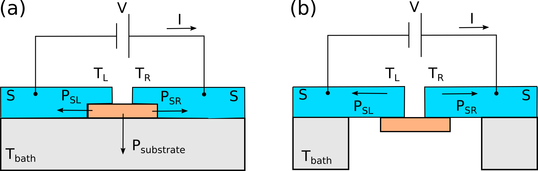
where we have introduced the bath temperature and the cooling power of the junction , which is, in general, unknown. The Joule heating power is partially carried away to the superconducting leads, while the rest of it goes to the substrate phonons and possibly to some other cooling channels, see Fig. 1(a). Here we assume that the junction resistance is much larger than the resistances of the leads and, hence, the Josephson critical current of the junction is much lower than the depairing current in the leads. In this case, at certain bias voltage the contact temperature becomes equal to the critical temperature of the superconductor, . At this point the differential conductance has a dip. Tracing the position of this dip at different bath temperatures, one can restore the cooling power as a function of .
We now find the shape of the dip close to the critical voltage value . In the vicinity of this bias point one can linearize Eq. (4) writing it in the form
| (5) |
Here is the thermal conductance of the leads at the critical temperature. According to the theory by Bardeen, Cooper and Schrieffer (BCS) [45], in the vicinity of the critical temperature the superconducting gap behaves as
| (6) |
where denotes Riemann’s zeta function. Combining this expression with the expression for the I-V curve (1), we transform Eq. (5) to the form
Solving this equation for , substituting the result in the expression for the current (1) and taking the derivative of it over , we obtain a simple analytical expression for the differential conductance
| (7) |
Here is the Heaviside step function and we have introduced the dimensionless parameter
| (8) |
The approximation (7) is formally valid if and . However, Eq. (7) can also be used outside this voltage interval because the non-linear correction to almost vanishes there. Eq. (7) predicts strong dip in the differential conductance with the negative minimum value, , which is achieved at . In the experiment, the dip is smeared by the inhomogeneity of the hot spot in the contact area between the leads and the central section, by the inverse proximity effect suppressing the gap close to the contact, etc.
In reality the two superconducting leads of the junction are never fully identical. They may have different critical temperatures, different geometry, and different couplings to the central section. As a result, a single dip in splits into two dips occurring at different bias voltages and , at which the left and the right leads switch to the normal state. In this case Eq. (4) cannot be solved analytically. However, in the limit one can rather accurately approximate the solution by the sum of two independent dips,
| (9) | |||||
For a symmetric case and for Eq. (9) coincides with the exact Eq. (7) everywhere except a narrow interval close to the minimum of the dip. Eq. (9) is valid for both positive and negative bias and it assumes that the two dips are sufficiently close so that one can use the same parameter (8) for both of them.
II.1 Suspended symmetric junction
In this subsection we consider a suspended junction in a symmetric configuration, in which the only cooling mechanism is the removal of heat through the superconducting leads, see Fig. 1b. This model can be easily solved numerically, and it allows us to test the analytical approximation (7). By symmetry, the power is dissipated in each lead. We assume that the right lead has the shape of a one-dimensional wire with the cross-sectional area , although the final expression for the cooling power of the junction (13) given below, does not depend on geometry of the lead thanks to the Wiedemann–Franz law relating heat and electric currents. Then, the temperature profile in the right lead is determined by the heat diffusion equation
| (10) |
where the themal conductivity of the lead is [46],
| (11) |
Here we have introduced the conductivity of the superconducting material in the normal state . We assume that the contact with the non-superconducting central part is located at so that , and at the superconducting wire contacts the bulk lead kept at the bath temperature, . Integrating Eq. (10) from to , we obtain the equation for the contact temperature ,
| (12) |
where
| (13) |
is the power carried away by quasiparticles through both superconducting leads. In Eq. (12) we introduced the total resistance of the two leads in the normal state . In this model, the heat conductance at critical temperature is determined by Wiedemann–Franz law, , and the dimensionless parameter (8) acquires the form
| (14) |
Next, from Eq. (12) we find the value of the critical voltage at low bath temperatures ,
| (15) |
where we have numerically evaluated the cooling power assuming the BCS dependence . Assuming that the excess current is fully suppressed for , one finds the critical power as , which gives
| (16) |
Interestingly, Eqs. (15,16) agree with many experimetal observations reported in the literature. Indeed, experiments in finite magnetic field [22] have shown that the critical voltage is proportional to the superconducting gap, , and the experiments with tip-shaped superconducting electrodes [24, 25] demonstrated that it is proportional to the square root of the interfacial resistance (). Eq. (16) predicts that the critical power does not depend on the junction resistance in agreement with the experiment [23]. We also note that at sufficiently low temperatures Eq. (15) may also be applicable to junctions lying on the substrate if the overheated leads have much higher heat conductance than the substrate.
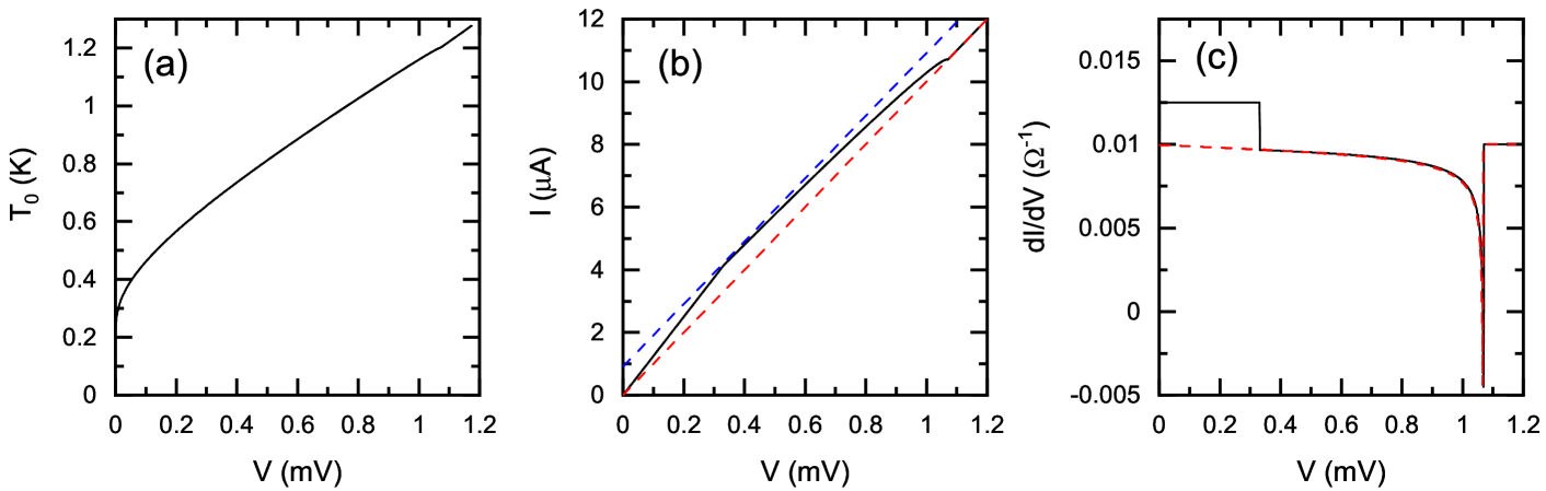
In Fig. 2 we present numerically exact results obtained from Eq. (12). We have chosen and approximated the I-V curve as follows: for , and for . We have ignored MAR features at sub-gap voltages because we focus at voltages above the double gap, . Voltage dependence of the contact temperature and of the current are shown in Figs. 2(a) and 2(b) respectively. In Fig. 2(c) we compare the exact differential conductance with the approximate expression (7) and observe perfect agreement between them for all voltages .
Finally, we provide approximations for the quasiparticle cooling power (13) at low and at high temperatures. Eq. (13) can be re-written in the form
| (17) |
where at low temperatures the function is exponentially small,
| (18) |
while at temperatures slightly below and for it takes the form
| (19) |
The first term in the right hand side of Eq. (19) corresponds to the Wiedemann–Franz heat current through the normal leads, and the second term describes a small correction to it caused by superconductivity onset at temperatures below .
III Experiment
Our back-gated devices were fabricated using exfoliated graphene on a SiO2/Si wafer. The substrate was highly boron-doped Si (p++/B, mcm) which remains conducting down to mK temperatures. A layer of dry oxide with a thickness of nm was grown thermally on the substrate at a temperature of 1000∘C. Before depositing graphene, alignment markers were patterned on the chips using optical lithography and evaporation of Ti and Au.
For suspended samples, we made graphene exfoliation on LOR resist [47]. After making the electrical contacts using electron beam lithography, the area to be suspended was irradiated using a high dose of electrons, developed in ethyl lactate, and washed in hexane. The electrical leads were made of aluminum/titanium sandwich structures. Titanium was evaporated at ultra high vacuum conditions which resulted in high transparency contacts to graphene. The presence of Ti lowered the superconducting transition temperature of the leads: in our second sample structure with a trilayer sandwich structure 10/50/10 nm of Ti/Al/Ti, the critical temperature was suppressed to half of the bulk value. The normal state resistance of the Al leads is m, which means that the Joule heating by the measurement current will mostly take place in the SGS junction. For details of the structure and dimensions of the two samples see Table I.
| type | leads | (nm) | (K) | |||||
|---|---|---|---|---|---|---|---|---|
| NS | ML | 0.30 | 6.0 | Ti/Al/Ti | 10/50/10 | 0.6 | 2 | 0.58 |
| S | BL | 0.50 | 1.0 | Ti/Al | 10/70 | 1.2 | 4 | 0.77 |
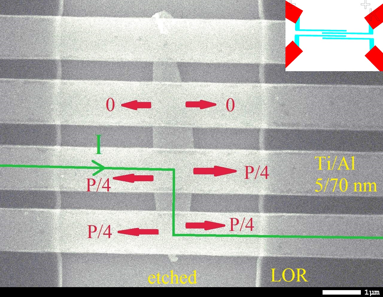
The suspended sample (S in Table I) with four measurement leads is illustrated in Fig. 3. The width of measurement leads is 1.2 m, i.e. the contact areas are more than two times larger than the size of the actual suspended part of the graphene. The bright looking sections of the horizontal leads in Fig. 3 are also suspended. Thus, the Joule heating generated in graphene has to propagate along suspended metallic leads over a distance of at least two microns before any cooling by the substrate through the LOR resist may take place. The arrows in the figure illustrate the flow of electrical current as well as the main directions of Joule heat escape from the sample. The critical temperature was slightly different for the four leads and the obtained values varied between mK (expected BCS gap eV).
Measurements were carried out using two dilution refrigerators: a BlueFors prototype cryostat BF-SD125 and a commercial BlueFors BF-LD250. Most of the measurements were performed on the BF-LD250 cryostat with the lowest achievable base temperature of approx. 10 mK. Temperatures were measured with a RuO2 resistor that had been calibrated against a Coulomb blockade thermometer [48]. An electrically shielded room with filtered power lines was employed to prevent electromagnetic interference and low-frequency electrical noise from affecting the weak signals before amplification. To limit the amount of thermal noise entering from room temperature to the sample, all dc lines were equipped with three-stage low-pass filters at the base temperature of the cryostat, with a cut-off frequency of kHz.
The electrical characteristics were obtained using regular low-noise measurement methods and lock-in techniques. We employed current bias through M resistor, selected on the basis of the required current range (dependent on gate voltage ). The voltage across the sample was measured using an LI-75 low-noise preamplifier powered from lead batteries. Differential resistance at small audio frequency (around 70 Hz) was measured simultaneously with the DC characteristics using a Stanford SR830 lock-in amplifier.
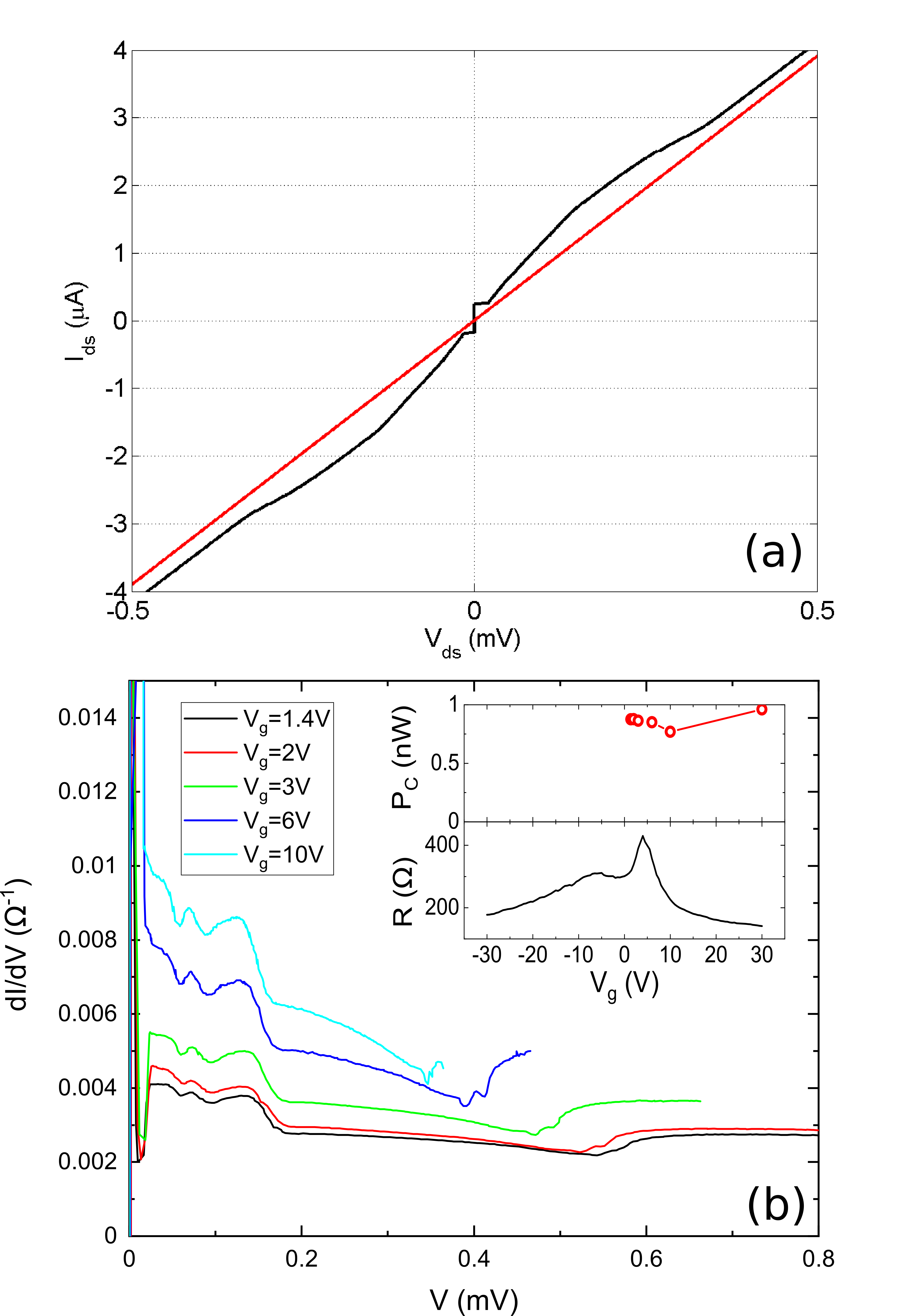
In Fig. 4(a) we show the I-V curve of the non-suspended SGS junction taken at low bath temperature mK. This junction has rather large excess current exceeding the Josephson critical current. For this reason, its suppression at high bias voltage is clearly visible. The experimental I-V curve resembles the theoretical one plotted in Fig. 2(b), although in the experiment only one of the leads completely switches to the normal state in presented range of bias voltages. This junction exhibits large value of the pre-factor in the excess current, , which points to its high transparency. Assuming that the junction is long and diffusive, we can use Eq. (3) and estimate the ratio , which gives the coherence length nm. In Fig. 4(b) we plot the differential resistance of the same sample at several values of the gate voltage. It is evident that both the critical voltage and the junction resistance (see the inset) significantly vary with . However, as the inset shows, the critical power only weakly depends on and varies from 0.77 nW to 0.96 nW for the presented five values of the gate voltage. This obervation agrees with that of Ref. [23], and it is also consistent with Eqs. (15,16). We believe that the remaining weak dependence of on results from the incomplete suppression of the -dependent excess current above in this sample.
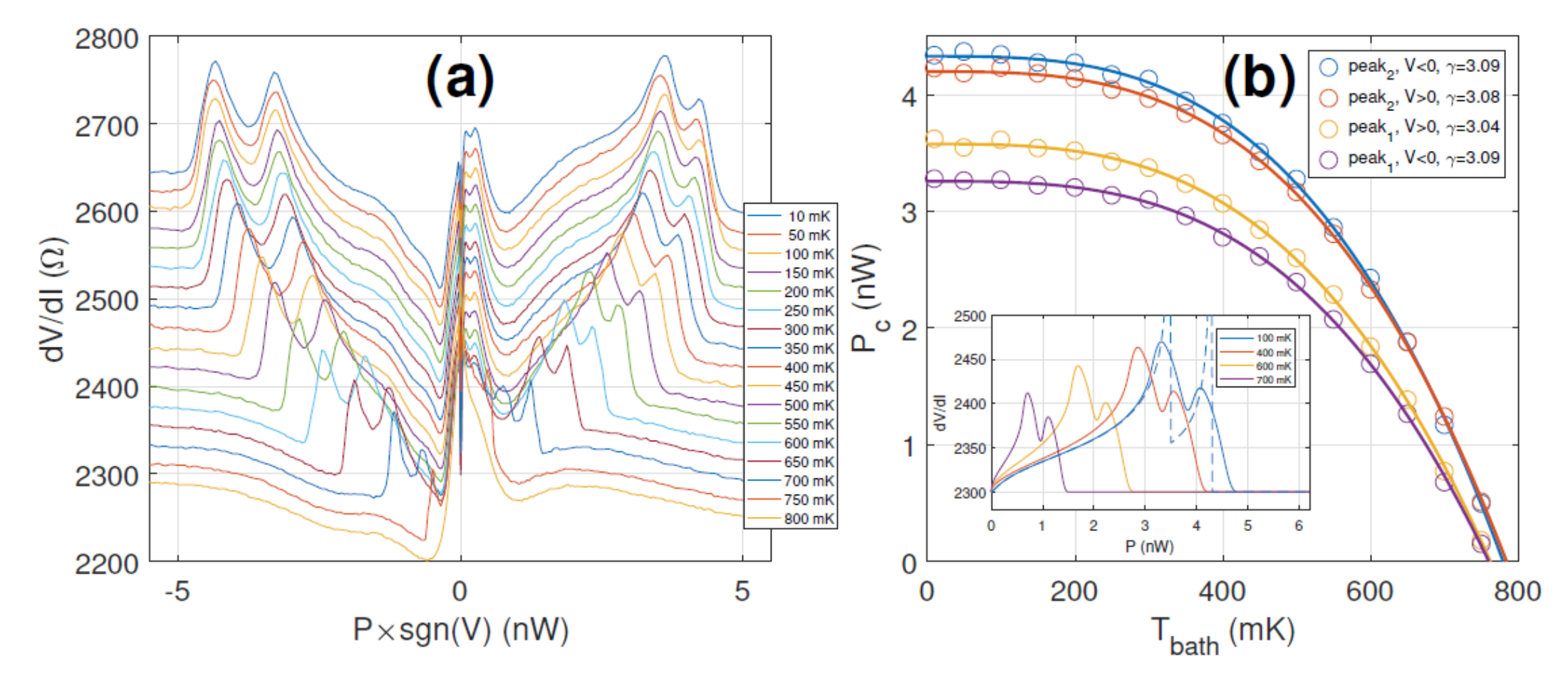
The superconducting-to-normal transition due to Joule heating in a suspended bilayer SGS sample is depicted in Fig. 5a for a temperature range of mK ( mK). Each resistance peak is clearly split into two parts, presumably because of junction asymmetry. There is also a small asymmetry between positive and negative bias voltages, giving rise to a total of four peaks.
Heat flow in mesoscopic devices can typically be characterized by a power law of the form
| (20) |
where is a constant and is a characteristic exponent which depends on the dissipation mechanism. The transition to the normal state occurs at the critical temperature and the corresponding critical powers can be expressed as
| (21) |
where is the critical power at . The observed peak positions from Fig. 5(a) are plotted in Fig. 5(b), along with the fits using Eq. (21) and the exponent as a fit parameter. We obtain for all four peaks. The four resistance traces in Fig. 5(b) converge to two different critical temperatures, mK and mK. This supports the idea that the two leads have slightly different critical temperatures.
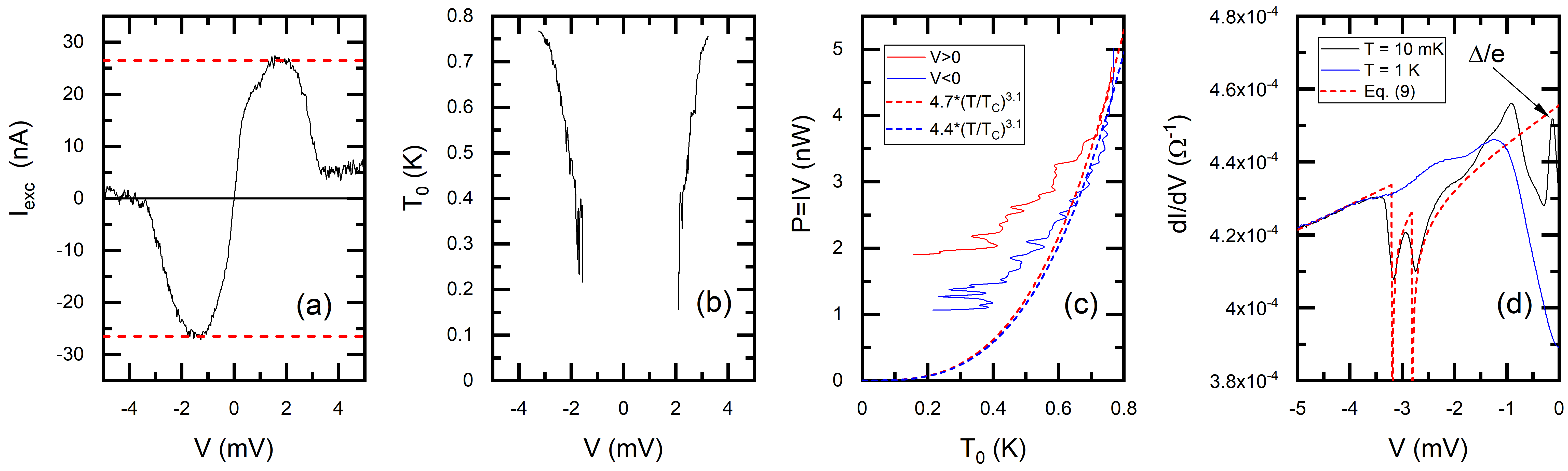
Next, we analyze the dependence of the differential conductance of the suspended SGS junction on bias voltage. First, we find bias dependent excess current by subtracting the IV-curves of the junction measured at the base temperature of mK, when the leads are superconducting, and at 1K, when the leads become normal, i.e. we define . This current is plotted in Fig. 6(a). Two red dashes lines show the maximum and the minimum value of , they are equal to nA and should correspond to the non-suppressed theoretical excess current defined in Eq. (1). Analyzing multiple Andreev reflection pattern in for this sample (see Fig. 6(d)), we estimate the superconducting gaps eV and find the junction resistance . With these values, we obtain the excess current suppression parameter from Eq. (1) as . From Eq. (3) we estimate the ratio and nm. The latter value is similar to the one obtained for the non-suspended junction, which supports the validity of the diffusive model for graphene.
In Fig. 6(b) we plot the effective temperature of the leads , which is obtained from the bias dependent excess current plotted in Fig. 6(a) by numerically solving the equation and assuming BCS gap-temperature dependence, . We used mK, which is the average value between the critical temperatures of the two leads given above. The accuracy of this procedure is limited by the noise in , which stems from the numerical subtraction of the two experimental I-V curves. For this reason, the splitting between the two critical voltages and , which is clear in Fig. 5(a), is not visible in Fig. 6(a). Therefore, here we ignore relatively weak asymetry between the leads and put . Furthermore, this type of thermometry only makes sense in the limited range of bias voltages where the excess current decreases with the bias, but the critical temperature of the leads is not yet reached. Therefore, only these two voltage intervals at positive and at negative bias are shown in Fig. 6(b). The dependence , obtained in this way, resembles the model prediction shown in Fig. 2(a).
In Fig. 6(c) we plot the Joule heating power , which is equal to the cooling power of the junction, versus the temperature of the leads presented in Fig. 6(b). The red line corresponds to the positive bias and the blue one – to the negative bias. The dashed lines present the predictions of Eq. (20) at very low bath temperature, , and with the same values of the exponent and as in the theory curves shown in Fig. 5(b). Namely, we have used nW for positive and nW for negative bias, and these values match those extracted from the positions of the peaks in with larger power, see Fig. 5(b). The agreement between the dashed lines and the experimental curves is good at relatively high temperatures close to . Thus, we have confirmed the validity of Eq. (20) in a broader range of temperatures by varying the temperature of the leads with the bias voltage and keeping the bath temperature temperature low, mK. At temperatures K the power law curves deviate from the experimetal data. However, there the accuracy of the numerical conversion of the excess current to temperature becomes very poor and we cannot draw any conclusion from this discrepancy.
The differential conductances of the suspended SGS junction in the superconducting ( mK, black line) and in the normal ( K, blue line) states are presented in Fig. 6(d). We show only negative bias voltages, where the dips associated with the transition of the leads to the normal state are more prononced. In the same figure we also show the fit based on Eq. (9) with the red dashed line. The theoretical curve has been plotted with the paramters earlier extracted from the fits shown in Figs. 5(b) and 6(a), namely, we have used , and nW. With these parameters, we obtain the thermal conductance at critical temperature nW/K. To obtain this value, we have taken the derivative of the cooling power (20) at and, as before, have set and K. The parameter , defined in Eq. (8), takes the value . The two critical voltages were adjustable parameters, they were chosen as mV and mV. In addition, we also introduced the non-linear correction to the differential conductance of the junction in the normal state, which originated from the energy dependent density of states in graphene and was needed to better reproduce the voltage dependence of the blue line in Fig. 6(d). Accordingly, in Eq. (9) we have replaced with mV-1. We find that Eq. (9), modified in this way, rather well reproduces the shape of the experimental -curve everywhere except at low bias voltages, where the MAR peaks become visible. As expected, the dips caused by transistion of the leads to the normal state are smeared in the experimental curve. We also note that Fig. 6(d) is a different representation of the inset in Fig. 5(b), and that it resembles the theoretical model plot of Fig. 2(c).
We conclude this section by noticing that the model of Sec. II, which relates the dips in the differential conductance of a highly transparent Josephson junction to the suppression of the excess current by Joule heating, well describes our experimental data.
IV Discussion and conclusions
In the previous section we have demonstrated how one can obtain the dependence of the cooling power of the Josephson junction on the bath temperature and on the junction temperature by fitting its differential conductance at high bias voltages above . This simple technique is applicable to any highly transparent Josephson junction and it might be useful for high-flux calibration of bolometers containing such junctions.
Our experimental results on graphene deserve further specific discussion. We find that the critical Joule heating becomes independent of the bath temperature at , see Fig. 5(b). Such saturation of the heat flow at low temperature is rather common in systems with weak coupling between electrons and lattice phonons. We find similar behavior in the theoretical electronic heat transport model of Sec. II.1. Indeed, for and at , where the energy gap of the superconductor does not depend on temperature, the heat power (13) saturates at the limiting value (16).
According to Figs. 4(a) and 5(b), the saturated low-temperature critical power amounts to nW and nW in our non-suspended and suspended sample, respectively. If we scale these values by the number of leads (see Table I) and the cross sectional area of the sandwich conductors, , we obtain the values kW/m2 and kW/m2. The similarity of these two critical power densities supports the conclusion that thermal transport along the leads is the main mechanism of heat relaxation in our devices.
The critical voltages amount to mV and mV for samples NS and S, respectively. We have applied Eq. (15) at low to investigate whether these values scale according to the model. Since we do not know exactly the lead resistance, we compare the measured ratio of critical voltages to the theory by assuming that the lead resistance scales inversely proportional to the cross sectional area of the leads [49]. With the parameters from Table I, Eq. (15) yields for the critical voltage ratio , while from the experimental data in Figs. 4 and 5 we obtain . Thus, our theoretical model accounts for the variation of the critical voltage within a range covering one order of magnitude.
The observed exponent in the temperature dependence of the power for the suspended junction, , is close to the one found by Borzenets et al for SGS junctions with Pb leads and graphene deposited on Si/SiO2 substrate [50]. Lead has a large superconducting gap, which should effectively cut off electronic thermal conductance below 1 K and leave only electron-phonon coupling for energy relaxation [52]. For SGS junctions with Al/Ti leads on the Si/SiO2 substrate the exponents [23] and [51], which agrees with our findings, have been previously reported. Power law thermal transport with the exponent has also been observed in superconducting Nb at low temperatures [53].
The origin of the exponent observed in our suspended device is not fully clear. Let us briefly discuss several possible explanations for this observation. In our experiment the ratio extends to large values, and, therefore, energy relaxation should be dominated by quasiparticles carrying heat through the leads. For temperatures close to the quasiparticles behave almost as normal state electrons obeying Wiedemann-Franz law, which leads to , see Eq. (19). The increase of the exponent from 2 to 3 may be qualitatively explained by several different effects or by their combination. First, the quasiparticle heat current (13) is lower and more sensitive to temperature than the normal state one in the whole interval , including the temperatures close to as Eq. (19) shows. Second, the parameter , appearing in the cooling power (13), is the resistance of the part of an Al lead in which thermalization between the quasiparticles and the substrate phonons occurs. Since the corresponding thermalization length is reduced with increasing temperature, the resistance is also reduced. Hence, the dependence of the power (13) on temperature becomes stronger than it were in the model with fixed . Yet another possibility for the increase of the exponent is the injection of strongly non-equilibrium quasiparticles with non-thermal distribution in the Al leads at high bias voltages. The propagation of such quasiparticles should be described by the full set of kinetic equations with the inclusion of charge imbalance instead of just one Eq. (10). Quantitative analysis of the effects mentioned above goes beyond the scope of this paper. At the moment, the similarity of the exponents observed in our experiment and in Refs. [50, 51] remains puzzling.
In conclusion, we have analyzed, both theoretically and experimentally, the effect of Joule heating on the IV characteristics of highly transparent Josephson junctions. We have shown that the Joule heating supresses the excess current and induces dips in the differential conductance at bias voltages where the two leads switch to the normal state. We have derived simple analytical expressions for the shape of these dips and for their positions in a specific case of a suspended junction, which is cooled only through the leads. We have experimentally tested preditions of the theory by studing SGS junctions in both suspended and non-suspended configurations. Good agreement between the experiment and the theory is found. In the suspended junction we observe power law temperature dependence of the heat current with the exponent instead of theoretically expected exponential dependence (18) at low temperatures and power law scaling with at higher temperatures (19). Our work also indicates that excess current can be employed for thermometry in special cases.
Acknowledgements
Discussions with Manohar Kumar and Alexander Savin are gratefully acknowledged. This work was supported by the Academy of Finland projects 314448 (BOLOSE), 310086 (LTnoise) and 312295 (CoE, Quantum Technology Finland) as well as by ERC (grant no. 670743). This research project utilized the Aalto University OtaNano/LTL infrastructure which is part of European Microkelvin Platform (funded by European Union’s Horizon 2020 Research and Innovation Programme Grant No. 824109). A.L. is grateful to Väisälä foundation of the Finnish Academy of Science and Letters for scholarship. The work at HSE University (M.R.S. and A.S.V.) was supported by the framework of the Academic Fund Program at HSE University in 2021 (grant No 21-04-041).
References
- [1] W. Haberkorn, H. Knauer, and J. Richter, Phys. Status Solidi A47, K161 (1978).
- [2] A. A. Golubov, M. Yu. Kupriyanov, and E. Il’ichev, Rev. Mod. Phys. 76, 411 (2004).
- [3] M. Hays, G. de Lange, K. Serniak, D.J. van Woerkom, D. Bouman, P. Krogstrup, J. Nygard, A. Geresdi, and M.H. Devoret, Phys. Rev. Lett. 121, 047001 (2018).
- [4] A. Zazunov, V. S. Shumeiko, E. N. Bratus, J. Lantz, and G.Wendin, Phys. Rev. Lett. 90, 087003 (2003).
- [5] M. Octavio, M. Tinkham, G.E. Blonder, and T.M.Klapwijk, Phys. Rev. B 27, 6739 (1983).
- [6] J. C. Cuevas, A. Martin-Rodero, and A. Levy Yeyati, Phys. Rev. B 54, 7366 (1996).
- [7] A. Bardas and D.V. Averin, Phys. Rev. B 56, R8518 (1997).
- [8] D.V. Averin, G. Wang, and A.S. Vasenko, Phys. Rev. B 102, 144516 (2020).
- [9] X. Du, I. Skachko, and E. Y. Andrei, Phys. Rev. B 77, 184507 (2008).
- [10] W. Liang, M. Bockrath, D. Bozovic, J. H. Hafner, M. Tinkham, and H. Park, Nature 411, 665 (2001).
- [11] P. Jarillo-Herrero, J.A. van Dam, and L.P. Kouwenhoven, Nature 439, 953 (2006).
- [12] J-D. Pillet, C. H. L. Quay, P. Morfin, C. Bena, A. Levy Yeyati and P. Joyez, Nat. Phys. 6, 965 (2010).
- [13] V.E. Calado, S. Goswami, G. Nanda, M. Diez, A.R. Akhmerov, K. Watanabe, T. Taniguchi, T.M. Klapwijk, and L.M.K. Vandersypen, Nat. Nanotechnology 10, 761 (2015).
- [14] G.-H. Lee, S. Kim, S.-H. Jhi, H.-J. Lee, Nature Comm. 6, 6181 (2015).
- [15] S. Abay, D. Persson, H. Nilsson, F. Wu, H.Q. Xu, M. Fogelström, V. Shumeiko, and P. Delsing, Phys. Rev. B 89, 214508 (2014).
- [16] E.M. Spanton, M. Deng, S. Vaitiekenas, P. Krogstrup, J. Nygard, C.M. Marcus, and K.A. Moler, Nat. Phys. 13, 1177 (2017).
- [17] I. Sochnikov, L. Maier, C.A. Watson, J.R. Kirtley, C. Gould, G. Tkachov, E. M. Hankiewicz, C. Brüne, H. Buhmann, L.W. Molenkamp, and K.A. Moler, Phys. Rev. Lett. 114, 066801 (2015).
- [18] M. Veldhorst, M. Snelder, M. Hoek, T. Gang, V.K. Guduru, X.L. Wang, U. Zeitler, W.G. van der Wiel, A.A. Golubov, H. Hilgenkamp and A. Brinkman, Nat. Mat. 11, 417 (2012).
- [19] S. Charpentier, L. Galletti, G. Kunakova, R. Arpaia, Y. Song, R. Baghdadi, S.M. Wang, A. Kalaboukhov, E. Olsson, F. Tafuri, D. Golubev, J. Linder, T. Bauch, and F. Lombardi, Nat. Comm. 8, 2019 (2017).
- [20] G. E. Blonder, M. Tinkham, and T. M. Klapwijk, Phys. Rev. B 25, 4515 (1982).
- [21] Chanh Nguyen, Herbert Kroemer, and Evelyn L. Hu, Phys. Rev. Lett. 69, 2847 (1992).
- [22] Peng Xiong, Gang Xiao and R.B. Lebowitz, Phys. Rev. Lett. 71, 1907 (1993).
- [23] Jae-Hyun Choi, Hu-Jong Lee and Yong-Joo Doh, J. Korean Phys. Soc. 57, 149 (2010).
- [24] P. S. Westbrook and A. Javan, Phys. Rev. B 59, 14606 (1999).
- [25] J. A. Gifford, G. J. Zhao, B. C. Li, J. Zhang, D. R. Kim, and T. Y. Chen, J. Appl. Phys. 120, 163901 (2016).
- [26] K. Flensberg and J. Bindslev Hansen, Phys. Rev. B 40, 8693 (1989).
- [27] H. Courtois, M. Meschke, J. T. Peltonen, and J. P. Pekola, Phys. Rev. Lett. 101, 067002 (2008).
- [28] M. Tinkham, J. U. Free, C. N. Lau, and N. Markovic, Phys. Rev. B 68, 134515 (2003).
- [29] H. Vora, P. Kumaravadivel, B. Nielsen and X. Du, Appl. Phys. Lett. 100, 153507 (2012).
- [30] K. C. Fong, and K. Schwab, Phys. Rev. X 2, 031006 (2012).
- [31] J. Yan, et al., Nat. Nanotechnol. 7, 472–478 (2012).
- [32] C. McKitterick, D. Prober and B. Karasik, J. Appl. Phys. 113, 044512 (2013).
- [33] D. K. Efetov, et al., Nat. Nanotechnol. 13, 797–801 (2018).
- [34] Q. Han, et al., Sci. Rep. 3, 3533 (2013).
- [35] X. Cai, et al., Nat. Nanotechnol. 9, 814–819 (2014).
- [36] A. E. El Fatimy, et al., Nat. Nanotechnol. 11, 335–338 (2016).
- [37] G.-H. Lee, D.K. Efetov, W. Jung, L. Ranzani, E.D. Walsh, T.A. Ohki, T. Taniguchi, K. Watanabe, P. Kim, D. Englund and K.C. Fong, Nature 586, 42 (2020).
- [38] R. Kokkoniemi, J.-P. Girard, D. Hazra, A. Laitinen, J. Govenius, R. E. Lake, I. Sallinen, V. Vesterinen, M. Partanen, J. Y. Tan, K. W. Chan, K. Y. Tan, P. Hakonen and M. Möttönen, Nature 586, 47 (2020).
- [39] A.V. Zaitsev, Zh. Eksp. Teor. Fiz. 86, 1742 (1984) [Sov. Phys. JETP 59, 1015 (1984)].
- [40] M. Titov and C. W. J. Beenakker, Phys. Rev. B 74, 041401(R) (2006).
- [41] P. Joyez, D. Vion, M. Götz, M. H. Devoret, and D. Esteve, J. Supercond. 12, 757 (1999).
- [42] O. N. Dorokhov, Solid State Commun. 51, 381 (1984).
- [43] J. Tworzydlo, B. Trauzettel, M. Titov, A. Rycerz, and C.W.J. Beenakker, Phys. Rev. Lett. 96, 246802 (2006).
- [44] J. C. Cuevas, J. Hammer, J. Kopu, J. K. Viljas, and M. Eschrig, Phys. Rev. B 73, 184505 (2006).
- [45] J. Bardeen, L.N. Cooper, and J.R. Schrieffer, Phy. Rev. 108, 1175 (1957).
- [46] J. Bardeen, G. Rickayzen, and L. Tewordt, Phys. Rev. 113, 982 (1959).
- [47] N. Tombros, A. Veligura, J. Junesch, J. J. van den Berg, P. J. Zomer, M. Wojtaszek, I. J. V. Marun, H. T. Jonkman, and B. J. van Wees, J. Appl. Phys. 109, 93702 (2011).
- [48] J. P. Pekola, K. P. Hirvi, J. P. Kauppinen, and M. A. Paalanen, Phys. Rev. Lett. 73, 2903 (1994).
- [49] The normal state resistance of the Al layer is much smaller than that of the Ti layer. Hence, we also checked the scaling using the Al layer thickness, but the difference is small, and the change would not modify our conclusions. We use the total thickness because the mechanism of the electronic heat transport in the superconducting state is not fully clear.
- [50] I. V. Borzenets, U. C. Coskun, H. T. Mebrahtu, Y. V. Bomze, A. I. Smirnov, and G. Finkelstein, Phys. Rev. Lett., 111, 027001 (2013).
- [51] K. Tsumura, N. Furukawa, H. Ito, E. Watanabe, D. Tsuya, and H. Takayanagi, Appl. Phys. Lett. 108, 033109 (2016).
- [52] J. Voutilainen, A. Fay, P. Häkkinen, J. K. Viljas, T. T. Heikkilä, and P. J. Hakonen, Phys. Rev. B, 84, 045419 (2011).
- [53] A. Feshchenko, O-P. Saira, J. Peltonen, J. P. Pekola, Sci Rep 7, 41728 (2017).