Lone pair driven anisotropy in antimony chalcogenide semiconductors
Xinwei Wang
Department of Materials, Imperial College London, Exhibition Road, London SW7 2AZ, UK
Zhenzhu Li
Department of Materials, Imperial College London, Exhibition Road, London SW7 2AZ, UK
Department of Materials Science and Engineering, Yonsei University, Seoul 03722, Korea
Seán R. Kavanagh
Department of Materials, Imperial College London, Exhibition Road, London SW7 2AZ, UK
Thomas Young Centre and Department of Chemistry, University College London, 20 Gordon Street, London WC1H 0AJ, UK
Alex M. Ganose
Department of Materials, Imperial College London, Exhibition Road, London SW7 2AZ, UK
Aron Walsh
a.walsh@imperial.ac.uk
Department of Materials, Imperial College London, Exhibition Road, London SW7 2AZ, UK
Department of Materials Science and Engineering, Yonsei University, Seoul 03722, Korea
Abstract
Antimony sulfide (\ceSb2S3) and selenide (\ceSb2Se3) have emerged as promising earth-abundant alternatives among thin-film photovoltaic compounds. A distinguishing feature of these materials is their anisotropic crystal structures, which are composed of quasi-one-dimensional (1D) [Sb4X6]n ribbons. The interaction between ribbons has been reported to be van der Waals (vdW) in nature and Sb2X3 are thus commonly classified in the literature as 1D semiconductors. However, based on first-principles calculations, here we show that inter-ribbon interactions are present in Sb2X3 beyond the vdW regime. The origin of the anisotropic structures is related to the stereochemical activity of the Sb 5s lone pair according to electronic structure analysis. The impacts of structural anisotropy on the electronic, dielectric and optical properties relevant to solar cells are further examined, including the presence of higher dimensional Fermi surfaces for charge carrier transport. Our study provides guidelines for optimising the performance of Sb2X3-based photovoltaics via device structuring based on the underlying crystal anisotropy.
††preprint: AIP/123-QED
PV
photovoltaic
CIGS
copper indium gallium selenide
CdTe
cadmium telluride
CZTS
copper zinc tin sulfide
CZTSe
copper zinc tin selenide
CZTSSe
copper zinc tin sulfoselenide
PCE
power conversion efficiency
GBs
grain boundaries
DLTS
deep-level transient spectroscopy
ODLTS
optical deep-level transient spectroscopy
TAS
thermal admittance spectroscopy
ITS
isothermal transient spectroscopy
SQ
Shockley–Queisser
SRH
Shockley–Read–Hall
vdW
van der Waals
VASP
Vienna Ab initio Simulation Package
DFT
density functional theory
LZ
Lany and Zunger
FNV
Freysoldt, Neugebauer and Van de Walle
KO
Kumagai and Oba
1D
one-dimensional
3D
three-dimensional
PDOS
projected density of states
COHP
crystal orbital Hamilton populations
VB
valence band
CB
conduction band
VBM
valence band maximum
CBM
conduction band maximum
PESs
potential energy surfaces
DFPT
density functional perturbation theory
I Introduction
Solar photovoltaic (PV) technology which converts the solar energy into electricity provides a clean and sustainable solution to the energy crisis. Current commercial thin-film light absorber materials such as cadmium telluride (CdTe) and copper indium gallium selenide (CIGS) have achieved certified PV efficiencies of over 20% under laboratory conditions[1]. However, CdTe suffers from the scarcity of Te elements and toxicity of Cd elements, while in CIGS the cost of In and Ga elements is too high, which limit their large-scale applications. As potential alternatives, antimony chalcogenides (Sb2X3; X=S, Se) have attracted growing attention. Sb2X3 have advantages of long-term stability, optimal bandgaps and high absorption coefficients (>105 cm-1) with abundant, non-toxic and low-cost constituents[2, 3, 4].
The PV conversion efficiencies of Sb2X3 devices have increased rapidly during the last decade. The current record efficiencies for pure Sb2S3 and Sb2Se3 have reached 7.5 and 9.2 respectively[5, 6]. However, these values are still far below the maximum theoretical efficiency of 30 predicted by the Shockley–Queisser (SQ) model[7] which is an idealised model only based on band gaps of solar absorbers.
Intensive efforts have been devoted to improve the efficiencies in Sb2X3 solar cells. One research direction is the orientation control of Sb2X3 films[8, 9].
Based on the understanding that Sb2X3 are composed of one-dimensional (1D) [Sb4X6]n ribbons which are held together by vdW forces[10, 11, 12, 13, 14], it has been reported that higher PV efficiency could be achieved when the Sb2X3 films are oriented more perpendicular to the substrate due to more efficient carrier transport along ribbons than between them[15].
Consequently, researchers have focused on tailoring the growth orientation of Sb2X3 films in order to achieve high efficiencies[16, 17, 18, 6, 19].
However, the origin of anisotropic crystal structures and the connection to physical properties remains unclear.
Building on recent work that has shown a tolerance to structural reconstructions[20],
understanding how film orientations affect the conversion efficiency in Sb2X3 is crucial to designing high-performance devices.
In this study, we investigate the anisotropic structural, electronic and optical properties of Sb2X3 using first-principles calculations. The dimensionality of Sb2X3 is studied by consideration of the chemical binding energies, carrier effective masses, and Fermi surfaces. Electronic structure analysis further confirms that the anisotropic crystal structures of Sb2X3 result from the stereochemical activity of the Sb 5s lone pair. Moreover, anisotropic optical properties including dielectric constants and optical absorption spectra are reported.
II Methods
Analysis of the total energy and electronic structure was performed within the framework of Kohn-Sham density-functional theory (DFT)[21, 22]. Calculations were performed based on DFT as implemented in the Vienna Ab initio Simulation Package (VASP)[23].
The projector augmented-wave (PAW) method[24] was employed with a plane-wave energy cutoff of 400 eV. All calculations were carried out using the Heyd-Scuseria-Ernzerhof hybrid functional (HSE06)[25, 26] except for the calculation of ionic contribution of dielectric constants, as a lower-level functional is sufficient for this high-cost calculation[27].
To account for the weak inter-ribbon interactions, the optB86b-vdW functional[28] was used to calculate the ionic contribution to the static dielectric constant, and the D3 dispersion correction[29] was used for HSE06 calculations.
The coefficients used for the zero-damping D3 correction are consistent with the previous research[30]. In order to obtain well-converged structures, the atomic positions were optimised until the Hellman-Feynman forces on each atom were below 0.0005 eV Å-1, and the energy convergence criterion was set to 10-8 eV. According to convergence tests (shown in Table. S2), the total energies of Sb2S3 and Sb2Se3 converge to within 1 meV/atom at a k-point mesh of 722. Therefore, -centered k-point meshes were set to 722 for geometry optimisation with primitive unit cells, and 1444 for projected density of states (PDOS) and crystal orbital Hamilton populations (COHP) calculations. For calculations of effective masses, dielectric constants and optical absorption coefficients which are more sensitive to k-point density, detailed settings and the proof of convergence are shown in the SI (Table S3-S6).
The crystal structures and partial charge densities were plotted using CrystalMaker®[31]. The PDOS and optical absorption spectra were plotted using the sumo package[32]. COHP calculations were performed using the LOBSTER package[33]. Fermi surfaces were plotted using the IFermi package[34]. The conductivity effective mass tensors were calculated by the AMSET package[35]. The conductivity effective mass (m∗) is obtained based on Boltzmann transport theory[36, 37] and is defined as[38]:
(1)
Where is the conductivity, n is the carrier concentration, e is the electron charge and is the carrier life time, in this work set to 10-14 s. The ionic contribution to the static dielectric constants was calculated by density functional perturbation theory (DFPT)[39], while the electronic part was calculated using the approach developed by Furthmüller et al. [39] The optical absorption coefficients () were calculated from the dielectric function by the sumo package[32] using the equation:
(2)
Where and are the frequency and wavelength of the incident light, respectively. k() is the extinction coefficient defined as
(3)
Where 1 and 2 are the real and imaginary parts of the high-frequency dielectric constants, respectively. The figures of distance histograms, COHP, dielectric constants, optical absorption spectra and thickness-dependent maximum efficiencies were plotted using matplotlib[40].
III Results and discussions
III.1 Structural properties
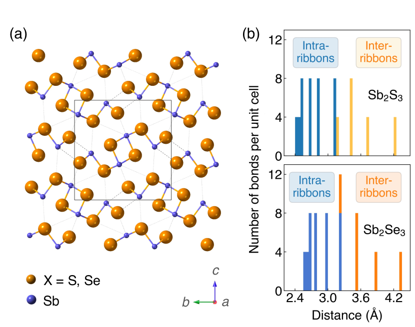
The ground-state crystal structures of Sb2S3 and Sb2Se3 (Pnma space group) are shown in Fig. 1a. They are composed of strongly bonded quasi-1D [Sb4X6]n ribbons units stacked together by weak interactions. In order to better reproduce the crystal structures, different vdW dispersion correction methods were applied in the geometry optimisation process. Lattice parameters calculated by different functionals and different vdW correction methods and obtained by experiments[41, 42, 43, 44, 45, 46] are shown in Table 1.
The c parameter (the direction between ribbons) is significantly overestimated ( 7.0) with no dispersion correction included for both PBE and HSE06 functionals. Including dispersion corrections, the accuracy of lattice parameter in the c direction is greatly improved regardless of the correction methods.
This demonstrates the presence of significant vdW interactions between ribbons, which are much weaker than the bonding within ribbons, and thus the necessity of dispersion corrections when modelling Sb2X3. For both systems, HSE06+D3 gives the best agreement with experimental measurements (an average difference of 0.7 % and 0.9 % for Sb2S3 and Sb2Se3 from the experimental lattice constants, respectively), which is in agreement with previous studies [30, 47], followed by optB86b performing the next best (1.0 % and 1.4 % difference for Sb2S3 and Sb2Se3 , respectively). Thus, the HSE06 functional with the D3 Grimme dispersion correction was used for most of the following calculations and the optB86b functional was used for most convergence tests.
Table 1: Lattice parameters (Å) of Sb2S3 and Sb2Se3 as calculated by different functionals and different vdW dispersion correction methods. The percentage error (%) relative to the experimental average is given in parentheses
Figure 1: (a) Crystal structures (Pnma space group) and (b) histogram of Sb-X distances of Sb2S3 and Sb2Se3. The unit cells are represented by rectangles.
Histograms of distances between Sb and X ions are shown in Fig. 1b. The widely distributed bond lengths indicate the anisotropic connectivity of Sb2X3. The bond lengths of Sb2Se3 are slightly larger than those of Sb2S3 due to the increased anion radius.
In the study of Deringer et al[48], analysis of the integrated COHP and the harmonic force constants showed a clear separation between strong intra-ribbon and weaker inter-ribbon interactions in \ceSb2Se3.
In order to quantify the interaction between ribbons, inter-ribbon binding energies () (per unit cell) along the b and c directions are calculated by
(4)
(5)
where and are total energies of one 1D [Sb4X6]n ribbon in isolation and one 2D [Sb4X6]n ribbon periodically repeated along a and b directions, respectively (the 1D and 2D substructures are given in Fig. S1). is the total energy of the unit cell. The parameter 2 in Eq. 5 is due to the fact that one unit cell of Sb2X3 contains two [Sb4X6]n ribbons. Note that the substructures were directly taken from the optimised structures and kept unrelaxed in order to avoid structural distortion effects, as is typical for binding energy calculations[49, 50]. The effect of optimisation was also tested and the was 0.1 eV lower after the relaxation of substructures, which does not qualitatively influence the results. The choice of N depends on whether is defined as per atom or per bond. Table 2 shows the calculated using the HSE06 functional and D3 dispersion correction. It can be seen that of Sb2S3 and Sb2Se3 are both over 10 kJ·mol-1, which are both beyond the typical vdW regime (0.4 4 kJ·mol-1)[51]. This is consistent with previous research that the distance of Sb-S between ribbons in Sb2S3 is shorter than the sum of Sb and S vdW radii at 293 K[41]. Moreover, is larger than due to the elongation of ribbons along b, and the of Sb2Se3 is slightly larger than that of Sb2S3. The calculated values agree well with previous calculations[52] and indicate that the inter-ribbon interactions of Sb2S3 and Sb2Se3 are both between the vdW and covalent regime. The results of without vdW corrections are given in Table S1.
System
per bond
per bond (N=16)
per atom (N=20)
Sb2S3
27.44
15.96
12.77
Sb2Se3
31.13
17.95
14.36
Table 2: Inter-ribbon binding energies (kJ·mol-1) of Sb2S3 and Sb2Se3
III.2 Electronic properties
The strength of the interaction between ribbons is closely related to the distortion of Sb which originates from the stereochemically active Sb 5s lone pairs. Before going further into the lone pair analysis, the density of states and orbital overlaps are first investigated.
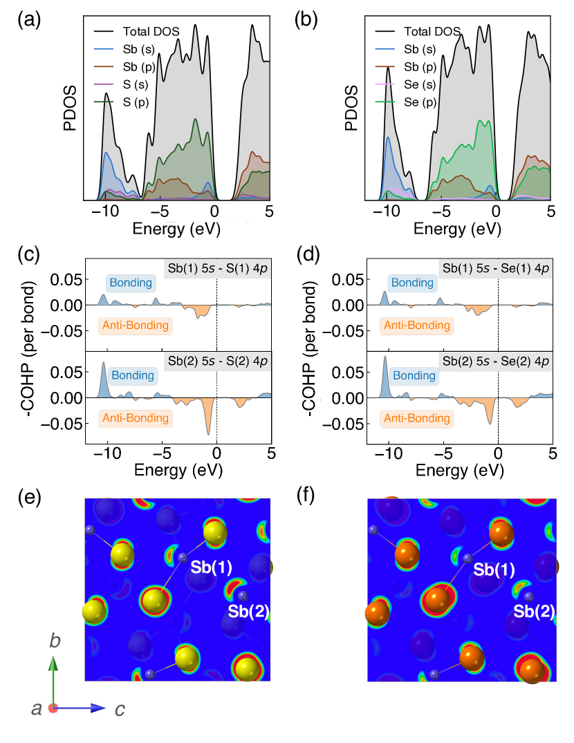
Figure 2: (a)-(b) Projected density of states (PDOS), (c)-(d) crystal orbital Hamilton populations (COHP) and (e)-(f) partial charge densities of antimony chacogenides. The range of isosurface value for partial charge densities is set to 0.05 0.10 e/Å3 for both Sb2S3 and Sb2Se3. The VBM is set to 0.
The PDOS are shown in Fig. 2a and 2b. The valence band (VB) can be divided into two main parts. The highest occupied VB between -1 and 0 eV consists of S 3p/Se 4p, Sb 5s and Sb 5p states. While the states between -10 and -7 eV mainly consists of Sb 5s orbitals, alongside some small contributions from S 3s/Se 4s and S 3p/Se 4p states. A valley at about 2 eV below the valence band maximum (VBM) is demonstrated to be one of the major characteristics of energy distribution curves for Sb2Se3 according to the photoemission measurements[46]. Our calculated PDOS of Sb2Se3 also shows a valley at -2 eV which is in good agreement with the experimental results. The conduction band (CB) are dominated by Sb 5p and S 3p/Se 4p states. These results agree well with earlier studies of PDOS on Sb2X3[53, 54, 48, 55].
The bonding and antibonding interactions are further studied by COHP[33] (shown in Fig. 2c and 2d). Two separate cases are plotted since Sb has two distinct chemical environment. The interaction is weaker in Sb(1)-X(1) than Sb(2)-X(2) which agrees with the longer bond lengths of Sb(1)-X(1). Combined with the results of PDOS, the energy range from -10 to -7 eV corresponds to a bonding interaction between Sb 5s and S 3p/Se 4p states, whereas the region at the top of the VB corresponds to an antibonding state, which is similar to other quasi-1D systems with stereochemically active lone pairs [56]. The photoemission measurements for Sb2Se3 [46] show that the lower part of VB below -6 eV is contributed by bonding states which agrees well with our results. Moreover, the interaction is stronger in Sb2S3 than Sb2Se3 which will be discussed in detail later.
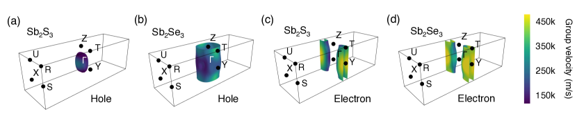
Figure 3: Fermi surfaces of Sb2S3 and Sb2Se3. (a) and (c) are hole Fermi surfaces (0.1 eV below the valence band maximum (VBM)), while (b) and (d) are electron Fermi surfaces (0.1 eV above the conduction band minimum (CBM)). The different colors represent the magnitude of group velocity (m/s)
The different inter-ribbon interactions in Sb2S3 and Sb2Se3 result from the Sb 5s lone pair formation. In the revised lone pair model[57], the interaction between the antibonding states of cation s - anion p and cation p states results in the formation of stereochemically active lone pairs. Smaller energy difference between cation s and anion p states will facilitate stronger interaction and thus stronger lone pair formation. In our systems, for the Sb(III) oxidation state found in \ceSb2X3, the formal electronic configuration of Sb is 5s25p0. Based on the discussions above, the Sb 5s states interact with the S 3p/Se 4p states in the VB forming filled bonding and anti-bonding states.
The additional interaction of the nominally empty Sb 5p orbitals stabilises the system by lowering the total energy, which is similar to other lone pair systems[58, 57, 59, 60].
The resulting stereochemically active lone pair results in an asymmetric electronic density at the top of VB which can be visualised by the contour plot of partial charge density. Partial charge densities for the states between -1 and 0 eV (with respect to the VBM) are shown in Fig. 2e and 2f. They are obtained by cutting the (100) plane through Sb atoms. The lone pair is stronger in Sb2S3 compared with Sb2Se3 due to the smaller energy separation and increased overlap of Sb 5s and S 3p.
To connect the electronic structure to transport properties, effective masses of electrons and holes were calculated (shown in Table 3). According to the electronic band structures of Sb2S3 and Sb2Se3 (shown in Fig. S2), the band dispersions around the extrema are relatively flat which are far from parabolic, and several extrema in different parts of the Brillouin Zone which are close in energy could be involved in contributing to conductivity. Therefore, effective masses in Sb2X3 are quite sensitive to calculation parameters (particularly the k-point density), and effective masses larger than 2 are rounded to the nearest whole numbers in Table 3 and S3. The harmonic mean is used to average the values for a polycrystalline sample with random orientations, and the anisotropy ratio () is defined as the ratio of maximum to minimum effective mass. The average effective masses of holes are larger than those of electrons for both Sb2S3 and Sb2Se3, indicating that Sb2S3 and Sb2Se3 may be better n-type semiconductors. Nevertheless, the electron effective masses show a stronger anisotropy. is larger in Sb2Se3 than Sb2S3 for both electron and hole effective masses, suggesting Sb2Se3 has stronger anisotropy which agrees with the weaker lone pair in Sb2Se3. The electron and hole effective masses are the largest along [001] for both Sb2S3 and Sb2Se3, indicating the conductivity between ribbons will be lower than along the other two directions. In general the values follow the trend xyz, with the exception of the hole effective mass for \ceSb2Se3, which is discussed later. Moreover, the 2D nature of transport (with small effective masses in two directions and large effective mass in the other direction) is similar to other so-called “quasi-1D” systems such as BiSI and BiSeI[61]. Our calculated effective masses deviate largely from other studies on Sb2X3[62, 63]. One possible reason of the discrepancy could be the use of simple parabolic fitting or the consideration of solely the point in other computational investigations. The choice of functionals could be another important factor, as demonstrated by Whalley et al. [64] It has been demonstrated that semi-local functionals would not only underestimate the bandgap, but also would influence the shape of band structures, resulting in overestimated nonparabolicity.
System
x
y
z
Sb2S3
m/m0
0.16
0.92
5
0.40
31.25
m/m0
0.47
0.65
0.97
0.64
2.06
Sb2Se3
m/m0
0.14
0.81
7
0.35
50.00
m/m0
0.85
0.55
3
0.90
5.45
Table 3: Effective masses of Sb2S3 and Sb2Se3. The harmonic mean is represented by . The anisotropy ratio () is defined as the ratio of maximum to minimum effective mass.
To further illustrate the dimensionality of the electronic structure, Fermi surfaces were plotted at 0.1 eV below (above) the VBM (CBM) using the IFermi package[34] (shown in Fig. 3). 0.1 eV is an arbitrary value intended to indicate the shape of the Fermi surface close to the band edge. Due to the tails of the Fermi-Dirac distribution, this energy range will be occupied at room temperature and the Fermi surface is therefore reflective of the states that govern transport properties. The Fermi surfaces of 0.08 and 0.12 eV below (above) the valence band maximum (conduction band maximum) were also shown in Fig. S3 and S4 which qualitatively show the same behaviour. An ellipsoidal Fermi surface is found for holes in \ceSb2S3 (Fig. 3a), indicating dispersion in three dimensions[65].
The shape of elliptical cylinders found for electrons in \ceSb2S3 (Fig. 3c) can be classified as quasi-2D with small dispersion in the [001] direction[65].
These agree well with observation that the hole effective mass of Sb2S3 is much smaller than the electron effective mass in the [001] direction.
In contrast, the hole and electron Fermi surfaces of Sb2Se3 are both quasi-2D (shown in Fig. 3b and 3d).
It can be seen that the electron Fermi surfaces of Sb2S3 and Sb2Se3 have similar topology, which indicates similar transport behaviour, whereas their hole Fermi surfaces have a significant difference in terms of the dimensionality.
Indeed, for \ceSb2S3 the three components of the effective mass are all below one, while for \ceSb2Se3 the z component is greater than 3.
We link this behaviour to the stronger lone pair distortion of Sb2S3 and the resulting shorter inter-ribbon Sb-S bonds along the [001] direction.
III.3 Optical properties
The dielectric constants are important descriptors for the optical properties of crystals.
The static dielectric constant (0) is defined as the sum of the ionic and high-frequency response to an external electric field. The complex dielectric function is given by:
(6)
Where 1 and 2 are the real part and imaginary part of the frequency-dependent dielectric function, respectively. For orthorhombic structures, the dielectric tensor has three distinct non-zero components.
As shown in Table 4, the dielectric constants of Sb2X3 are anisotropic and relatively large, which is common in lone-pair containing crystals[60, 56]. Large dielectric constants indicate the potential for strong screening to charged defects and low recombination losses[66, 67]. It can be seen that the dielectric constants are larger in the x and y directions than the z direction, indicating the screening is stronger in the ab plane. Moreover, the dielectric screening in Sb2X3 is shown to be dominated by the lattice polarization as the ionic contribution is much larger than the electronic contribution. The large ionic dielectric constants can be attributed to large Born effective charges in Sb2X3[68, 69].
The anisotropy ratio () (defined as the ratio of maximum to minimum dielectric constant) is larger in Sb2Se3 than Sb2S3 for both static and high-frequency dielectric constants, indicating Sb2Se3 has stronger anisotropy which is consistent with previous discussions.
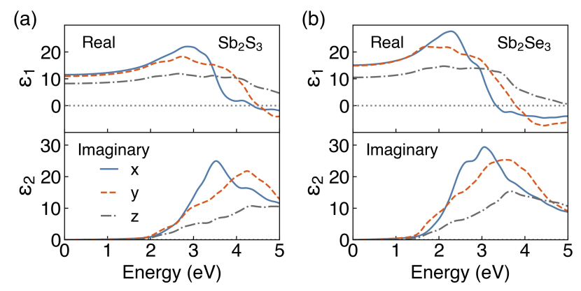
The real and imaginary parts of the high-frequency (∞) dielectric functions are plotted in Fig. 4. Combined with the results of PDOS, the peaks in the imaginary parts of dielectric functions mainly correspond to the optical transition from the S 3p/Se 4p states in the valence band to the Sb 5p states in the conduction band. Our calculated dielectric constants are in excellent agreement with ellipsometry measurements on polycrystalline thin films ( and of 12.5, 10.8 and 7.0 for Sb2S3 [70], respectively, and an averaged of 14.3 for Sb2Se3 [2]). Furthermore, our results are inline with previous theoretical studies [71, 72, 54, 73, 74].
System
0
∞
x
y
z
x
y
z
Sb2S3
98.94
94.21
13.14
7.53
11.55
10.97
8.25
1.40
Sb2Se3
85.64
128.18
15.00
8.54
15.11
14.92
10.53
1.43
Table 4: Calculated static (0) and high-frequency (∞) dielectric constants of Sb2S3 and Sb2Se3. The anisotropy ratio () is defined as the ratio of maximum to minimum dielectric constant.
Figure 4: Calculated high-frequency dielectric functions of (a) Sb2S3 and (b) Sb2Se3.
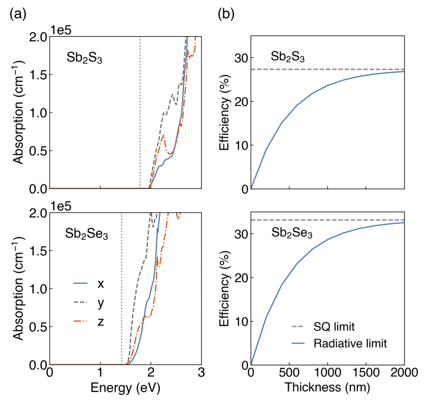
The calculated optical absorption spectra, and upper limit to photovoltaic efficiency, for Sb2S3 and Sb2Se3 are shown in Fig. 5. As can be seen in Fig. 5a, both Sb2S3 and Sb2Se3 possess high optical absorption coefficients above the band edge (in the range of 105 cm-1) which could more effectively absorb photons and generate electron-hole pairs. This agrees well with experimental UV-vis measurements on Sb2X3, which observed large absorption coefficients of 105 cm-1 in the visible region[4, 75, 76, 66]. Possible reasons for such high optical absorption coefficients in these indirect gap semiconductors could be attributed to their unique electronic band structures (shown in Fig. S2). On the one hand, the difference between indirect and direct gaps of Sb2X3 is small (0.16 eV for Sb2S3 and 0.06 eV for Sb2Se3) which make them still suitable for strong absorption near the band edges [77]. On the other hand, the relatively flat dispersions near the band extrema will lead to high DOS near the VBM and CBM and thus strong absorption [78]. Moreover, there is slight difference in absorption coefficients along different directions. The thickness-dependent radiative efficiencies (Fig. 5b) further show the same trend regardless of different orientations, which results from the relatively large absorption coefficients and the same value of the optical band gap along different directions. The radiative efficiencies are larger in Sb2Se3 than Sb2S3 since the band gap of Sb2Se3 is closer to the optimal band gap predicted by the SQ model. For both Sb2S3 and Sb2Se3, the radiative efficiencies approach the SQ limit at a thickness of 2 m. The results above indicate that absorption is not a limiting factor in the conversion efficiencies along different directions in Sb2S3 and Sb2Se3. Other effects such as defects and interfaces should be further considered in order to improve the efficiency in Sb2X3.
Figure 5: (a) Calculated optical absorption spectra of Sb2S3 and Sb2Se3. The fundamental band gaps are shown in grey dotted lines. (b) Thickness-dependent maximum efficiencies based on the radiative limit of Sb2S3 and Sb2Se3.
IV Conclusions
The standard description of \ceSb2X3 in the literature refers to them as 1D semiconductors, where electrons and holes can readily diffuse along, but not between, ribbons in the crystal. This has lead to a focus on thin-film synthesis to achieve optimal [100] orientations.
Our first-principles investigation has shown that the chemical binding energies between ribbons (>10 kJ·mol-1) falls between the vdW and ionic/covalent regime.
Analysis of the carrier effective masses does reveal a strong anisotropy, but the behaviour is not 1D, with stronger dispersion found in [010] compared to [001].
The Fermi surfaces for electrons and holes illustrate this complexity with a combination of 3D (holes in \ceSb2S3) and quasi-2D transport.
The anisotropy carries through to the dielectric response of the crystals with much stronger screening in the ab plane compared to along the c axis.
However, the resulting optical absorption profiles are less sensitive and yield the same radiative limit for photovoltaic applications.
The origin of these anisotropic effects is linked to lone pair formation associated with the filled Sb 5s orbitals which distorts the Sb coordination environment.
Acknowledgements
We are grateful to the UK Materials and Molecular Modelling Hub for computational resources, which is partially funded by EPSRC (EP/P020194/1 and EP/T022213/1). Xinwei Wang acknowledges Imperial College London for the funding of a President's PhD Scholarship. Seán R. Kavanagh acknowledges the EPSRC Centre for Doctoral Training in the Advanced Characterisation of Materials (CDT-ACM)(EP/S023259/1) for funding a PhD studentship. Alex M. Ganose was supported by EPSRC Fellowship EP/T033231/1. Xinwei Wang thanks Chengcheng Xiao and Sunghyun Kim for advice on the computational analysis.
Green et al. [2020]
M. A. Green, E. D. Dunlop, J. Hohl-Ebinger, M. Yoshita, N. Kopidakis and A. W.
Ho-Baillie, Progress in Photovoltaics: Research and Applications,
2020, 28, 3–15.
Chen et al. [2015]
C. Chen, W. Li, Y. Zhou, C. Chen, M. Luo, X. Liu, K. Zeng, B. Yang, C. Zhang,
J. Han et al., Appl. Phys. Lett., 2015, 107,
043905.
Ghosh and Varma [1979]
C. Ghosh and B. Varma, Thin solid films, 1979, 60, 61–65.
Zhou et al. [2014]
Y. Zhou, M. Leng, Z. Xia, J. Zhong, H. Song, X. Liu, B. Yang, J. Zhang,
J. Chen, K. Zhou et al., Adv. Energy Mater., 2014, 4,
1301846.
Choi et al. [2014]
Y. C. Choi, D. U. Lee, J. H. Noh, E. K. Kim and S. I. Seok, Adv. Funct.
Mater., 2014, 24, 3587–3592.
Li et al. [2019]
Z. Li, X. Liang, G. Li, H. Liu, H. Zhang, J. Guo, J. Chen, K. Shen, X. San,
W. Yu et al., Nat. Commun., 2019, 10, 1–9.
Shockley and Queisser [1961]
W. Shockley and H. J. Queisser, J. Appl. Phys., 1961, 32,
510–519.
Kim et al. [2021]
J. Kim, S. Ji, Y. Jang, G. Jeong, J. Choi, D. Kim, S.-W. Nam and B. Shin,
Sol. RRL, 2021, 5, 2100327.
Hobson et al. [2020]
T. D. Hobson, L. J. Phillips, O. S. Hutter, H. Shiel, J. E. Swallow, C. N.
Savory, P. K. Nayak, S. Mariotti, B. Das, L. Bowen et al., Chem.
Mater., 2020, 32, 2621–2630.
Caruso et al. [2015]
F. Caruso, M. R. Filip and F. Giustino, Phys. Rev. B, 2015, 92,
125134.
Song et al. [2017]
H. Song, T. Li, J. Zhang, Y. Zhou, J. Luo, C. Chen, B. Yang, C. Ge, Y. Wu and
J. Tang, Adv. Mater., 2017, 29, 1700441.
Guo et al. [2018]
L. Guo, B. Zhang, Y. Qin, D. Li, L. Li, X. Qian and F. Yan, Sol. RRL,
2018, 2, 1800128.
Yang et al. [2018]
W. Yang, J. Ahn, Y. Oh, J. Tan, H. Lee, J. Park, H.-C. Kwon, J. Kim, W. Jo,
J. Kim et al., Adv. Energy Mater., 2018, 8,
1702888.
Gusmão et al. [2019]
R. Gusmão, Z. Sofer, J. Luxa and M. Pumera, ACS Sustain. Chem. Eng.,
2019, 7, 15790–15798.
Zhou et al. [2015]
Y. Zhou, L. Wang, S. Chen, S. Qin, X. Liu, J. Chen, D.-J. Xue, M. Luo, Y. Cao,
Y. Cheng et al., Nat. Photonics, 2015, 9,
409–415.
Yuan et al. [2016]
S. Yuan, H. Deng, D. Dong, X. Yang, K. Qiao, C. Hu, H. Song, H. Song, Z. He and
J. Tang, Sol. Energy Mater. Sol. Cells, 2016, 157,
887–893.
Wang et al. [2017]
L. Wang, D.-B. Li, K. Li, C. Chen, H.-X. Deng, L. Gao, Y. Zhao, F. Jiang,
L. Li, F. Huang et al., Nat. Energy, 2017, 2,
1–9.
Kondrotas et al. [2019]
R. Kondrotas, J. Zhang, C. Wang and J. Tang, Sol. Energy Mater. Sol.
Cells, 2019, 199, 16–23.
Zeng et al. [2020]
Y. Zeng, K. Sun, J. Huang, M. P. Nielsen, F. Ji, C. Sha, S. Yuan, X. Zhang,
C. Yan, X. Liu et al., ACS Appl. Mater. Interfaces, 2020,
12, 22825–22834.
McKenna [2021]
K. P. McKenna, Adv. Electron. Mater, 2021, 7, 2000908.
Kohn and Sham [1965]
W. Kohn and L. J. Sham, Phys. Rev., 1965, 140, A1133.
Dreizler and Gross [1990]
R. M. Dreizler and E. K. Gross, Density Functional Theory, Springer,
1990, pp. 245–271.
Kresse and Furthmüller [1996]
G. Kresse and J. Furthmüller, Phys. Rev. B, 1996, 54,
11169.
Kresse and Joubert [1999]
G. Kresse and D. Joubert, Phys. Rev. B, 1999, 59, 1758.
Heyd et al. [2003]
J. Heyd, G. E. Scuseria and M. Ernzerhof, J. Chem. Phys., 2003,
118, 8207–8215.
Krukau et al. [2006]
A. V. Krukau, O. A. Vydrov, A. F. Izmaylov and G. E. Scuseria, J. Chem.
Phys., 2006, 125, 224106.
Kavanagh et al. [2021]
S. R. Kavanagh, A. Walsh and D. O. Scanlon, ACS Energy Lett., 2021,
6, 1392–1398.
Klimeš et al. [2011]
J. Klimeš, D. R. Bowler and A. Michaelides, Phys. Rev. B, 2011,
83, 195131.
Grimme [2004]
S. Grimme, J. Comput. Chem., 2004, 25, 1463–1473.
Savory and Scanlon [2019]
C. N. Savory and D. O. Scanlon, J. Mater. Chem. A, 2019, 7,
10739–10744.
Ganose et al. [2018]
A. M. Ganose, A. J. Jackson and D. O. Scanlon, J. Open Source Softw.,
2018, 3, 717.
Dronskowski and Blöchl [1993]
R. Dronskowski and P. E. Blöchl, J. Phys. Chem., 1993, 97,
8617–8624.
Ganose et al. [2021]
A. M. Ganose, A. Searle, A. Jain and S. M. Griffin, J. Open Source
Softw., 2021, 6, 3089.
Ganose et al. [2021]
A. M. Ganose, J. Park, A. Faghaninia, R. Woods-Robinson, K. A. Persson and
A. Jain, Nat. Commun., 2021, 12, 1–9.
Ashcroft et al. [1976]
N. W. Ashcroft, N. D. Mermin et al., Solid State Physics,
1976.
Madsen and Singh [2006]
G. K. Madsen and D. J. Singh, Comput. Phys. Commun., 2006, 175,
67–71.
Gibbs et al. [2017]
Z. M. Gibbs, F. Ricci, G. Li, H. Zhu, K. Persson, G. Ceder, G. Hautier, A. Jain
and G. J. Snyder, NPJ Comput. Mater., 2017, 3, 1–7.
Gajdoš et al. [2006]
M. Gajdoš, K. Hummer, G. Kresse, J. Furthmüller and F. Bechstedt,
Phys. Rev. B, 2006, 73, 045112.
Hunter [2007]
J. D. Hunter, Comput. Sci. Eng., 2007, 9, 90–95.
Kyono et al. [2002]
A. Kyono, M. Kimata, M. Matsuhisa, Y. Miyashita and K. Okamoto, Phys.
Chem. Miner., 2002, 29, 254–260.
Savadogo and Mandal [1992]
O. Savadogo and K. Mandal, Sol. Energy Mater. Sol. Cells, 1992,
26, 117–136.
Salem and Selim [2001]
A. Salem and M. S. Selim, J. Phys. D, 2001, 34, 12.
Efthimiopoulos et al. [2013]
I. Efthimiopoulos, J. Zhang, M. Kucway, C. Park, R. C. Ewing and Y. Wang,
Sci. Rep., 2013, 3, 1–8.
Voutsas et al. [1985]
G. Voutsas, A. Papazoglou, P. Rentzeperis and D. Siapkas, Z. Kristallogr.
Cryst. Mater., 1985, 171, 261–268.
Hurych et al. [1974]
Z. Hurych, D. Davis, D. Buczek, C. Wood, G. Lapeyre and A. Baer, Phys.
Rev. B, 1974, 9, 4392.
Stoliaroff et al. [2020]
A. Stoliaroff, A. Lecomte, O. Rubel, S. Jobic, X. Zhang, C. Latouche and
X. Rocquefelte, ACS Appl. Energy Mater., 2020, 3,
2496–2509.
Deringer et al. [2015]
V. L. Deringer, R. P. Stoffel, M. Wuttig and R. Dronskowski, Chem. Sci,
2015, 6, 5255–5262.
Mounet et al. [2018]
N. Mounet, M. Gibertini, P. Schwaller, D. Campi, A. Merkys, A. Marrazzo,
T. Sohier, I. E. Castelli, A. Cepellotti, G. Pizzi et al., Nat.
Nanotechnol., 2018, 13, 246–252.
Björkman et al. [2012]
T. Björkman, A. Gulans, A. V. Krasheninnikov and R. M. Nieminen,
Phys. Rev. Lett., 2012, 108, 235502.
Garrett and Grisham [1999]
R. H. Garrett and C. M. Grisham, Biochemistry, 1999.
Filip et al. [2013]
M. R. Filip, C. E. Patrick and F. Giustino, Phys. Rev. B, 2013,
87, 205125.
Caracas and Gonze [2005]
R. Caracas and X. Gonze, Phys. Chem. Miner., 2005, 32,
295–300.
Koç et al. [2012]
H. Koç, A. M. Mamedov, E. Deligoz and H. Ozisik, Solid State Sci.,
2012, 14, 1211–1220.
Radzwan et al. [2017]
A. Radzwan, R. Ahmed, A. Shaari, A. Lawal and Y. X. Ng, Malays. J.
Fundam. Appl. Sci., 2017, 13, 285–289.
Ganose et al. [2016]
A. M. Ganose, K. T. Butler, A. Walsh and D. O. Scanlon, J. Mater. Chem.
A, 2016, 4, 2060–2068.
Walsh et al. [2011]
A. Walsh, D. J. Payne, R. G. Egdell and G. W. Watson, Chem. Soc. Rev.,
2011, 40, 4455–4463.
Walsh and Watson [2005]
A. Walsh and G. W. Watson, J. Solid State Chem., 2005, 178,
1422–1428.
Allen et al. [2013]
J. P. Allen, J. J. Carey, A. Walsh, D. O. Scanlon and G. W. Watson, J.
Phys. Chem. C, 2013, 117, 14759–14769.
Kavanagh et al. [2021]
S. R. Kavanagh, C. N. Savory, D. O. Scanlon and A. Walsh, Mater. Horiz.,
2021.
Ganose et al. [2018]
A. M. Ganose, S. Matsumoto, J. Buckeridge and D. O. Scanlon, Chem.
Mater., 2018, 30, 3827–3835.
Nasr et al. [2016]
T. B. Nasr, H. Maghraoui-Meherzi and N. Kamoun-Turki, J. Alloys Compd.,
2016, 663, 123–127.
Qiu et al. [2019]
W. Qiu, C. Zhang, S. Cheng, Q. Zheng, X. Yu, H. Jia and B. Wu, J. Solid
State Chem., 2019, 271, 339–345.
Whalley et al. [2019]
L. D. Whalley, J. M. Frost, B. J. Morgan and A. Walsh, Phys. Rev. B,
2019, 99, 085207.
Albert [2015]
S. G. Albert, PhD thesis, Technische Universität München,
2015.
Zeng et al. [2016]
K. Zeng, D.-J. Xue and J. Tang, Semicond. Sci. Technol., 2016,
31, 063001.
Walsh and Zunger [2017]
A. Walsh and A. Zunger, Nat. Mater., 2017, 16, 964–967.
Liu et al. [2014]
Y. Liu, K. T. E. Chua, T. C. Sum and C. K. Gan, Phys. Chem. Chem. Phys.,
2014, 16, 345–350.
Cheng et al. [2019]
Y. Cheng, O. Cojocaru-Mirédin, J. Keutgen, Y. Yu, M. Küpers,
M. Schumacher, P. Golub, J.-Y. Raty, R. Dronskowski and M. Wuttig, Adv.
Mater., 2019, 31, 1904316.
Schubert et al. [2004]
M. Schubert, T. Hofmann, C. Herzinger and W. Dollase, Thin Solid Films,
2004, 455, 619–623.
Nasr et al. [2011]
T. B. Nasr, H. Maghraoui-Meherzi, H. B. Abdallah and R. Bennaceur,
Physica B Condens. Matter., 2011, 406, 287–292.
Lakhdar et al. [2014]
M. H. Lakhdar, B. Ouni and M. Amlouk, Mater. Sci. Semicond. Process.,
2014, 19, 32–39.
Maghraoui-Meherzi et al. [2013]
H. Maghraoui-Meherzi, T. B. Nasr and M. Dachraoui, Mater. Sci. Semicond.
Process., 2013, 16, 179–184.
Lawal et al. [2018]
A. Lawal, A. Shaari, R. Ahmed and L. Taura, Curr. Appl. Phys., 2018,
18, 567–575.
Versavel and Haber [2007]
M. Y. Versavel and J. A. Haber, Thin Solid Films, 2007, 515,
7171–7176.
Lai et al. [2012]
Y. Lai, Z. Chen, C. Han, L. Jiang, F. Liu, J. Li and Y. Liu, Appl. Surf.
Sci., 2012, 261, 510–514.
Kondrotas et al. [2021]
R. Kondrotas, C. Chen, X. Liu, B. Yang and J. Tang, J. Semicond., 2021,
42, 031701.
Kumar et al. [2014]
M. Kumar, N. Umezawa and M. Imai, Appl. Phys. Express, 2014, 7,
071203.