Effect of manganese incorporation on the excitonic recombination dynamics in monolayer MoS2
Abstract
Using X-ray photoelectron spectroscopy (XPS), atomic force microscopy (AFM) and Raman spectroscopy techniques we investigate the incorporation of Manganese (Mn) in monolayer (1L)-MoS2 grown on sapphire substrates by microcavity based chemical vapor deposition (CVD) method. These layers are coated with different amount of Mn by pulsed laser deposition (PLD) technique and temperature dependent photo-luminescence (PL) spectroscopic study has helped us in understanding how such deposition affects the dynamics of excitonic recombination in this system. The study further reveals two distinctly different Mn-incorporation regimes. Below a certain critical deposition amount of Mn, thin Mn-coating with large area coverage is found on MoS2 layers and in this regime, substitution of Mo ions by Mn is detected through XPS. Dewetting takes place when Mn-deposition crosses the critical mark, which results in the formation of Mn-droplets on MoS2 layers. In this regime, substitutional incorporation of Mn is suppressed, while the Raman study suggests an enhancement of disorder in the lattice with the Mn-deposition time. From PL investigation, it has been found that the increase of the amount of Mn-deposition not only enhances the density of non-radiative recombination channels for the excitons but also raises the barrier height for such recombination to take place. The study attributes these non-radiative transitions to certain Mo related defects (either Mo-vacancies or distorted Mo-S bonds), which are believed to be generated in large numbers during Mn-droplet formation stage as a result of the withdrawal of Mn ions from the Mo-substitutional sites.
Monolayer (1L) MoS2, a two dimensional (2D) transition metal dichalcogenide (TMD), has become one of the most studied materials in the last decade for its unique electronic and optical propertiesmak1 , among which spin-valley couplingmak2 ; VP ; VP1 and direct band gap at the K-points of the Brillouin zonemak1 ; bs are the most important ones. Because of its direct band gap of 1.9 eV and large exciton binding energy, 1L-MoS2 offers high luminescence yield in the visible rangemak1 ; bs ; VP1 . Atomically thin size and flexible nature make the material a potential candidate for 3D integrated and flexible electronics of the future 3D_flex . Furthermore, there are multiple theoretical proposals that predict ferromagnetic behaviour even above room temperature in 1L-MoS2, when Mo is substituted by certain transition metal ions. Such a two dimensional dilute magnetic semiconductor (2D-DMS) has potential for injecting spin polarized excitons and carriers for future 2D spintronic and valleytronic devicesmagnet1 ; magnet2 ; magnet3 ; VP2 . Achieving controllable doping is one of the important requirements for any technology application of the material. However, doping of 1L-MoS2 is always onerous because of the strong bonding between Mo and S, which makes it almost inert for any substitutional reaction to take placeXPS1 ; bs . This has become even more challenging as the unambiguous detection of doping is extremely difficult in an atomically thin layer. Even though, there are efforts by various groups to incorporate different elements in 1L-MoS2 using varied means, such as chemical dopingch1 ; ch2 ; ch3 , physisorptiontherm ; ad2 ; ad3 ; ad4 , metal evaporationevap1 ; raman2 and ion irradiationion1 ; raman1 , a method for stable and sustainable doping of the layer is yet to be established. Previously, Zhang et al. have reported up to 2 atomic percentage of Manganese (Mn) doping in 1L-MoS2 by vapor phase deposition techniqueXPS2 . Mn incorporation has also been tried using Mn ion irradiation techniqueraman1 , which has been found to result in a large amount of structural defects in the lattice. More studies are needed to understand the mechanism of incorporation of Mn and other metals in 1L-MoS2. It is also important to investigate how the incorporation can influence the electrical, optical and magnetic properties of the layer.
Here, we present a detailed study of manganese doping in 1L-MoS2 through pulsed laser deposition (PLD) technique and its influence on the optical properties of the films, which are grown on sapphire substrates by microcavity based chemical vapor deposition (CVD) techniquepkm ; tailoring . Our investigation using high resolution X-ray photoelectron spectroscopy (XPS), atomic force microscopy (AFM), Raman and PL spectroscopy reveals two clearly distinct regimes of Mn-incorporation in 1L-MoS2. When the deposition amount is below a certain critical value, Mn islands covering large areas are found to be formed on MoS2 layers and substitution of Mo ions by Mn are observed. As the deposition amount goes beyond the critical value, dewetting leads to the formation of Mn-droplets on MoS2 layers. In this regime, substitutional incorporation of Mn is decreased, while the disorder in the lattice increases with the deposition time. PL study shows that Mn-deposition strongly influence the excitonic recombination dynamics by opening up non-radiative recombination channels. Both the density and the barrier height for such recombinations are found to increase with the amount of Mn-deposited. These non-radiative transitions are attributed to certain Mo related defects.
Strictly monolayer (1L) MoS2 films were grown on c-sapphire substrates by the microcavity based CVD route where molybdenum trioxide (MoO3) and sulfur (S) powders were used as precursors and argon (Ar) was used as the carrier gas. More details about the growth can be found elsewherepkm ; tailoring . Manganese (Mn) was deposited on these layers using pulsed laser deposition (PLD) technique where a polycrystalline Mn pellet was used as target. The pellet was prepared from 99.99% pure Mn powder by arc melting technique in Ar (5N pure) atmosphere. Substrate (1L-MoS2/sapphire) temperature was maintained at 300C during the deposition. Distance between the Mn-target and the sample was kept at 5 cm for all depositions. A KrF excimer laser of wavelength 248 nm and pulse width of 25 ns was used for ablating the target. Deposition amount was varied by varying the laser pulse count. While the pulse frequency and the energy density of the laser were maintained at 1 Hz and 1.4 J/cm2, respectively, for all cases. Base pressure inside the PLD chamber was kept at 8.010-5 mbar. During the growth, 5N argon gas was introduced inside the chamber to maintain a pressure of 8.010-2 mbar inside the chamber. 1L-MoS2 layers were coated with Mn for different numbers of laser pulse count ranging from 1 to 10. These samples are labeled by alphabets A to D. In another sample (sample E), Mn deposition was carried out at the base pressure ( 8.010-5 mbar) for 10 counts of laser pulses. Mn was also deposited on a bare c-plane sapphire substrate (without MoS2) for five counts of laser pulses at 8.010-2 mbar of Ar-pressure, keeping other parameters constant. This sample is named as sample F. One as-grown 1L-MoS2 sample R, was used as the reference standard for all the measurements. Mn deposition parameters for these samples, are listed in Tab. 1.
X-ray photoelectron spectroscopy on these samples were performed in Axis Supra spectrometer from Kratos Analytical, UK, where monochromatic Al Kα x-ray (h = 1486.6 eV) was used as excitation source. Energy axis of the recorded spectra, was calibrated with respect to the binding energy of carbon 1 peak at 284.7 eV. Morphology of the samples were examined by atomic force microscopy (AFM) in tapping mode using Bruker, NanoScope-IV system. Raman spectra on these monolayers were recorded at room temperature in back scattering geometry with 532 nm diode laser using Horiba Jobin Yvon HR800 confocal Raman spectrometer. A closed-cycle helium refrigerator was used to carry out temperature dependent (from 20 K to 300 K) photoluminescence (PL) measurements, where 532 nm diode laser was used as the excitation source and the spectra were recorded by a 0.55 m focal length monochromator attached with a Peltier cooled CCD camera.
| Sample | Pressure | Ar flow rate | Laser Pulse count |
| (mbar) | (sccm) | ||
| R | – | – | 0 |
| A | 8.010-2 | 40 | 1 |
| B | 8.010-2 | 40 | 5 |
| C | 8.010-2 | 40 | 7 |
| D | 8.010-2 | 40 | 10 |
| E | 8.010-5 | 0 | 10 |
| F (Sapphire) | 8.010-2 | 40 | 5 |
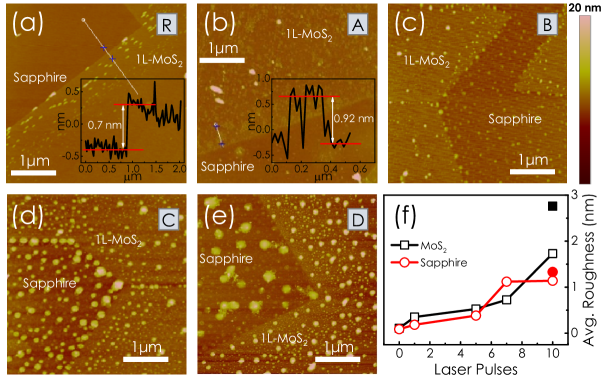
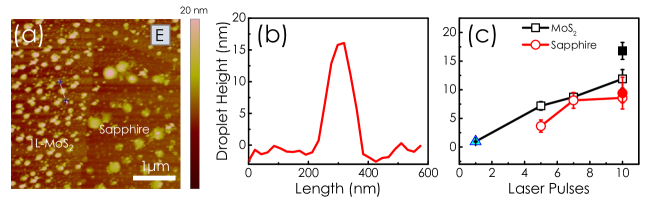
Fig. 1 shows AFM images for the MoS2 samples coated with Mn for different counts of laser pulses. In all the images, MoS2 layers can clearly be distinguished from the bare sapphire surface from the height contrast. As shown in Fig. 1(a), average step-height for the reference sample R has been found to be 0.7 nm, which is expected for a monolayer MoS2 pkm ; tailoring . In fact, it should be noted that average step-height for all samples before Mn deposition is found to be 0.7 nm confirming monolayer nature of MoS2 in all cases. As shown in Fig. 1(b), deposition of several flat island type structures with average height of 0.9 nm on the MoS2 regions is evident in sample A, where only one laser pulse is used for Mn deposition. In case of sample B, where Mn is deposited for 5 laser pulses, flat island type structures could not be distinguished clearly on MoS2 regions, instead, several spherical structures are visible on both MoS2 and bare sapphire regions as shown in Fig. 1(c). Density and size of the spherical droplets clearly increase as one moves from sample C [Fig. 1(d)] to D [Fig. 1(e)], meaning as the laser pulse count for Mn deposition increases (see supplementary Fig. S1sup ). Noticeably, in these samples, droplets on bare sapphire are bigger than those on MoS2 regions. It is noteworthy that similar type of droplet formation has also been observed in case of sample E (see supplementary Fig. S1sup ). Fig. 1(f) plots the average value of the roughness of MoS2 (black symbols) and sapphire (red symbols) regions as functions of laser pulse count. Evidently, variation of roughness on MoS2 regions shows a clear increase beyond 5 counts of laser pulse. Note that the average roughness on sapphire regions also shows a sudden jump beyond 5 pulses. These are consistent with the sudden change in the morphology observed in the AFM images and seem to suggest that Mn-deposition for sufficiently less number of laser pulses results in a thin Mn-layer. The strain/surface energy developed in such a thin metal film may not be sufficient to change its morphology when the sample is cooled to room temperature after deposition. It is plausible that in case of the samples, where Mn-deposition is performed for the number of pulses more than a certain value, thickness of the deposited Mn-film crosses a critical mark and the strain/surface energy developed in the layer becomes so high that to minimise energy, the film breaks into Mn-droplets when the sample is brought to the room temperature. This point has been discussed again later (in Fig. 5).
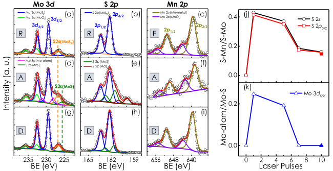
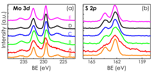
In panels (a-i) of Fig. 2, XPS spectra for Mo , S , S and Mn levels for different samples are compared. These spectra are deconvoluted with Voigt functions as mentioned in earlier referencesXPS ; XPS1 . In all panels, red lines represent the fitted profiles. For the reference sample R [panel (a)], S (orange line) peak appears (at 226.7 eV) along with Mo doublets. Mo related features can be deconvoluted into two doublets. While, the position of the first doublet, which peaks at 229.3 eV (Mo ) and 232.4 eV (Mo ) [blue line], matches quite well with Mo-S bonds in MoS2 XPS ; XPS1 , the second doublet appearing at 232.6 eV (Mo ), 235.7 eV (Mo ) [bright green line] can be assigned to the Mo-O bonds of the unreacted MoO3 particles on the surfaceXPS . Panel (b) shows the S features for the reference sample. Deconvolution of the feature results in two peaks centred at 162.2 eV and 163.4 eV, (blue line) which are associated with S and S lines, respectively, of MoS2 XPS ; XPS1 . Fig. 2(c) shows Mn features for sample F, which is a bare sapphire substrate coated with manganese. The feature can be deconvoluted into two doublets. While the doublet (olive line) appearing at 639.2 eV (Mn ) and 651.0 eV (Mn ) can be attributed to Mn-metalXPS2 ; XPS3 , position of the higher energy doublet (purple line) appearing at 644.0 eV (Mn ) and 655.6 eV (Mn ) matches quite well with those of Mn-O bonds of manganese oxide (MnOx)XPS2 ; XPS5 . Quite evidently, Mo , S as well as S features appears much broader for sample A as compared to the reference sample as can be seen in Fig. 2(d) and (e). This is a clear indication of the change of the bonding states of both Mo and S ions in this sample. Deconvolution of these features results in the formation of one additional Mo doublet peaking at 227.9 eV (Mo ) and 231.0 eV (Mo ) [magenta line in Fig. 2(d)], one extra S peak (at 225.5 eV) [bottle green line in Fig. 2(d)] and two extra S doublets; one peaking at 161.4 eV (S ) and 162.6 eV (S ) [bottle green line in Fig. 2 (e)] and the other, peaking at 159.9 eV (S ) and 161.0 eV (S )[brown line in Fig. 2(e)]. Position of the new Mo doublet [magenta line in Fig. 2 (d)] matches well with neutral Mo atomsXPS1 . Out of the two extra S doublets, the bottle green line of Fig. 2(e) can be assigned to S-Mn bond formation and the brown line of Fig. 2(e) can be attributed to surface adsorbed S atomsXPS1 . The extra S peak at 225.5 eV [bottle green line in Fig. 2(d)] can also be attributed S-Mn bondsXPS4 ; XPS2 . Interestingly for sample D, Mo , S and S profiles are similar to those obtained for the reference sample as shown in Fig. 2(g) and (h). Deconvolution of these profiles results in a much weaker contributions from the S-Mn bonds and neutral Mo atoms as compared to what has been found in case of sample A. These findings point towards the fact that for sample A, Mn atoms partially substitute Mo ions of MoS2 to form Mn-S bonds and the knocked out Mo ions settle as neutral Mo atoms. While, in sample D, such substitution is very weakly present. It should be noted that like in sample A, significant presence of additional Mo and S related features could also be found in sample B, where Mn is deposited for 5 laser pulses. Similar to the case of sample D, very weak sign of Mo-substitution by Mn-ions could be found for sample C and E, where laser pulse counts of 7 and 10, respectively, are used for Mn deposition. Note that Mo , S and S spectra for all the Mn deposited MoS2 samples are shown in supplementary figure S2sup . Fig. 2(f) and (i) show the Mn features for sample A and D, respectively. It is interesting to note that for both the cases, features are very similar to what has been found for sample F [Fig. 2(c)] showing the contributions only from Mn-metal and Mn-O bonds. In fact, no sign of Mn-S bond formation could be found from Mn-spectra for any of the Mn-coated MoS2 samples. Note that in all these samples, a significant portion of the sapphire surface remains uncovered by 1L-MoS2. Perhaps, the signal due to Mn-S bond from the Mn-coated MoS2 layers is overwhelmed by the signal arising from the Mn-coated sapphire regions for all these samples. The ratio of the contributions from S-Mn and S-Mo bonds can be obtained in two ways; by deconvoluting (i) S and (ii) S spectra. These results are plotted as a function of the laser pulse count in Fig. 2(j). Evidently, both the profiles show very similar trend. Similarly, the ratio of the contribution from Mo atoms and Mo-S bonds can be achieved from the Mo peaks, which is plotted versus pulse count in Fig. 2(k). Interestingly, no signature of knocked out Mo atoms could be found in samples deposited with more than 5 pulse counts. It is quite evident from these plots that substantial amount of Mo-substitutional incorporation of Mn in 1L-MoS2 layers is achieved only for pulse counts of 1 and 5. Incorporation sharply decreases as the pulse count goes beyond 5.
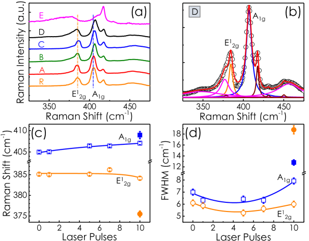
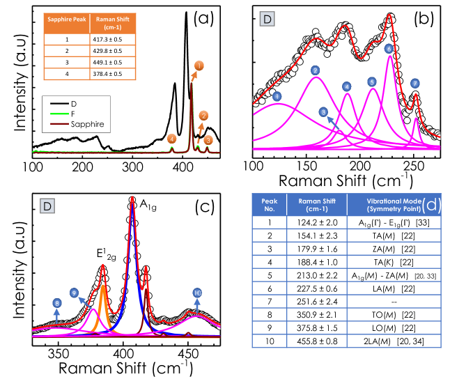
Fig. 3(a) compares room temperature micro-Raman spectra for these samples in the frequency range, where characteristic in-plane E and out-of-plane A1g vibrational modes for the zone-centre phonons are observed at 385 and 405 cm-1, respectively. These spectra are deconvoluted with Lorentzian functions as shown in the Fig. 3(b) for sample D as an example. Apart from the dominant E (orange line) and A1g (blue line) features, several other phonon modes associated with M and K points of the Brillouin zone (BZ) [magenta lines] can also be seen. Note that these non-zone-centre phonons become visible due to the relaxation of the fundamental Raman selection rule (phonon wave vector 0) in the presence of disorder in the MoS2 lattice (see supplementary Fig. S3sup )raman1 ; raman2 ; raman4 ; raman5 . There are also a couple of other features (brown lines) in the spectrum, which can be identified as the Raman lines arising from the sapphire substrate (see the supplementary Fig. S3sup ). Fig. 3(c) and (d) plot the peak position and full width at half maximum (FWHM) of the Lorentzians associated with E (orange) and A1g (blue) peaks as functions of the number of laser pulses used for Mn-deposition in these samples. It is evident from these figures that with the increase of pulse count, A1g peak shows a tendency of shift towards higher wavenumbers. On the other hand, position of E peak does not vary much with pulse count upto 7, beyond which it reduces. It should be noted that electron concentration in the conduction band has a strong influence on the coupling between electrons and A1g phonons in 1L-MoS2 raman3 . Increase of electron concentration in the layer is found to result in the softening of frequency as well as broadening of the A1g peak, while E feature hardly shows any changeraman1 ; raman2 ; raman3 . Note that the FWHM of the A1g peak is less than that of the reference sample for samples A and B, where the pulse counts are 1 and 5, respectively. This may suggest a reduction of electron concentration in the two MoS2 samples, which can further imply that Mn-ions incorporate in MoS2 when the number of laser pulses used for Mn deposition is sufficiently less. This observation is also consistent with the results of the XPS study shown in Fig. 2. Increasing trend of the line-width for both A1g and E peaks as well as hardening and softening of A1g and E modes, respectively, for pulse count beyond 7 may indicate a rise of disorder in the layer with the increase of Mn-deposition time.
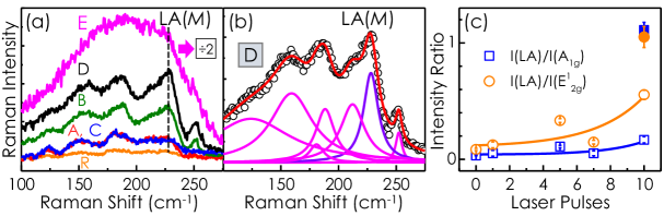
Fig. 4(a) highlights the lower energy portion of the Raman spectra for these samples, where certain zone edge phonons give rise to broad structure with multiple features due to the presence of disorderraman1 ; raman2 ; raman4 ; raman5 . Fig. 4(b) shows the Lorentzian deconvolution of the structure for sample D, where the most dominant peak at 227 cm-1 (violet line) has previously been assigned to longitudinal acoustic phonon mode at M point [LA(M)]. This peak has also been treated as a measure of disorder in 1L-MoS2 filmsraman1 . Please see supplementary Fig. S3sup for identification of other features in the structure. It should be noted that the spectra shown in all the above panels are normalized with respect to the intensity of A1g peak. From Fig. 4(a) it is evident that all the disorder related peaks enhance with the laser pulse count suggesting a gradual increase of disorder with the amount of Mn deposition in these samples. In case of sample E, where Mn-deposition is carried out for 10 pulse-counts in vacuum (switching off the Ar supply), peak-shift and peak-width for both E and A1g peaks are dramatically higher than the other samples suggesting much higher degree of disorder in this sample [see Fig. 3(c) and (d)]. Intensity ratios between LA(M) and A1g peaks [I(LA)/I(A1g)] (blue line) as well as LA(M) and E peaks [I(LA)/I(E)] (orange line), are plotted in Fig. 4(f). A gradual rise of disorder with increasing Mn-deposition time is quite evident from the figure. This observation is in line with the results shown in Fig. 3.
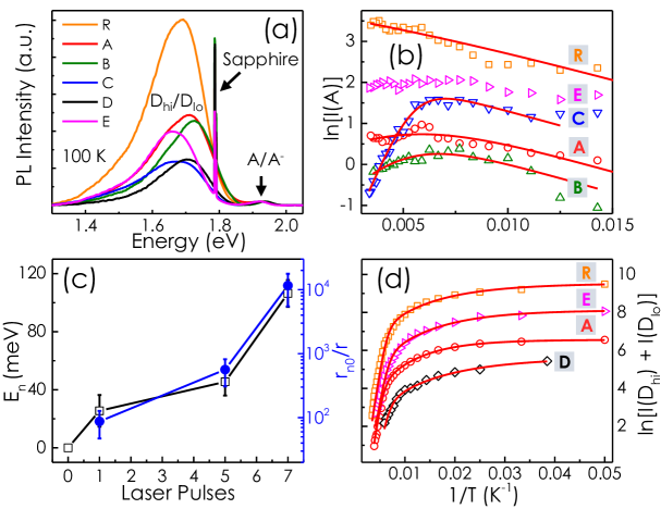
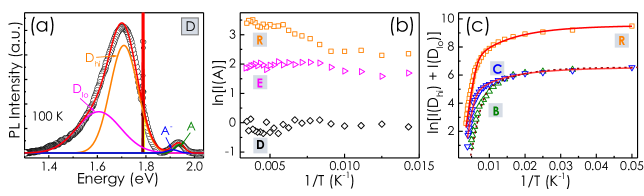
Fig. 5(a) compares photoluminescence (PL) spectra recorded at 100 K for all samples. Each spectrum is featured by a band-edge exciton/trion (A/A-) peak at 1.9 eV and broad luminescence (BL) peak at 1.7 eVpkm ; tailoring ; nihit1 . Deconvolution of these PL spectra by a set of six Gaussian peaks [as shown in the supplementary Fig. S4(a)sup ] provides a good fittailoring . Band edge feature is consisting of two Gaussians representing free A-excitons (A) and A-trions (A-), while the BL feature can be fitted with two Gaussian functions centred at 1.71 eV () and 1.6 eV (). and transitions are found to be excitonic in nature and attributed to sulfur vacancy related defectstailoring . Note that two narrow Gaussians are used to take into account the sharp feature at 1.78 eV that stems from the sapphire substrate. Temperature dependent PL spectra for all samples are recorded from 20 to 300 K and deconvoluted with six Gaussians as described before. Log of the intensity associated with A-exciton [] is plotted as a function of inverse of temperature in fig. 5(b), for various samples. In case of the reference sample R (orange), increases monotonically with temperature. This tendency indicates that the excitons are activated from a bound to free sate as temperature increases. For samples deposited with 1, 5 and 7 pulses of Mn, shows similar increasing tendency upto a certain temperature, beyond which it shows a reduction with rising temperature. This fall becomes increasingly steeper as the pulse count increases from 1 to 7. This result suggests that Mn-deposition might be introducing a non-radiative recombination channel for the A-excitons, which need to overcome a thermal barrier to get access to the non-radiative traps. Above finding further implies that the barrier height must be increasing with the amount of Mn deposited. In sample D, where Mn pulse count is 10, become almost temperature independent. In case of sample E, shows similar trend as sample D [see supplementary Fig. S4(b)sup ]. We believe that the thermal energy barrier for the non-radiative recombination is so high for the two samples that one needs to go to higher than room temperature to see the fall of A-exciton intensity. It should be noted that in samples D and E, the density of Mn-deposition induced disorder in MoS2 is expected to be much more than the rest of the samples as discussed in Fig. 4. At the steady state condition, density of free excitons () and excitons bound to type of defect () should satisfy the following equations.
| (1) |
Where, , and are , respectively, the rate of generation, radiative and non-radiative recombinations for the free excitons. is the concentration of type of defect traps and () is the coefficient of transition of an exciton from free (defect bound) state to defect bound (free) state. is the recombination rate of defect bound excitons. At thermal equilibrium, = . = , where and are activation energy of excitons from defect bound to free state and the height of the thermal energy barrier for non-radiative recombination, respectively. is the Boltzmann constant and is at = 0 K. Under the assumptions of and , the expressions for PL intensities associated with free excitons [= ] and the bound excitons[= ] can be obtained from eq. 1 as,
| (2) | |||
| (3) |
Experimentally obtained temperature variations of for all samples have been fitted by eq. 2. The resultant profiles are the red solid curves shown in fig. 5(b). The fit for the reference sample R returns = 12.4 meV and = 0. value is kept at 12.4 meV while is varied to fit the data for rest of the Mn-deposited samples. Obtained values for and are plotted as functions of pulse count in fig. 5(c). It can be seen that both the quantities gradually increase with the pulse count. Note that the increase of could suggest the enhancement of the density of non-radiative centres in the layer. As discussed before, and for sample D and E can not be estimated from this study. Fig. 5(d) plots logarithm of combined integrated intensities of and [ + ], i.e., total intensity of BL feature as a function of the inverse of temperature for sample R, A, D and E. Please refer to the supplementary Fig. S4(c)sup for vs plots for samples B and C. It can be seen that like in the reference sample, in all Mn-deposited samples, intensity of this feature increases and shows a tendency of saturation with the reduction of temperature. This result implies that the Mn disorder induced non-radiative recombination channel, which modifies the variation of intensity of A-exciton with temperature in these samples, does not affect the dynamics of the sulfur deficiency bound excitonic features. It should be noted that our attempts to simulate the data of Fig. 5(d) using eq. 3 with the parameters obtained from the fitting of the data using eq. 2 as shown in Fig. 5(b) have failed for every sample. This suggests that BL band has nothing to do with the defect D, which binds A-excitons in our model (eq. 1). This further means that BL transition does not directly involve A-excitons. To find the binding energies associated with and , experimental data of [ + ] vs are fitted with the equation below as described in our previous reporttailoring .
| (4) |
where, and are the binding energy and a measure of capture cross section of -th type of sulfur-vacancy related defects. Terms under summation in the denominator take into account the contributions from the of two defect bands, and . Temperature variation of the intensity of the defect bound BL feature is fitted with eq. 4 and the resultant profiles are represented by red solid curves in fig. 5(d). Values of ( 100 meV) and ( 5 meV) are found to be almost the same for all the samples. This confirms that Mn deposition does not affect the dynamics of sulfur deficiency related BL transition in these samples.
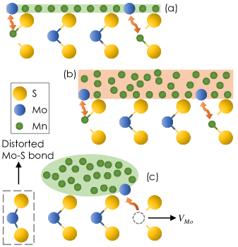
From Fig. 1 and 2 it appears that in the regime when Mn is deposited on MoS2 forming large flat-top islands (laser pulse count upto 5), Mo-substitutional incorporation of Mn in 1L-MoS2 is more than in the regime when Mn-droplets are formed. It is plausible that since the area coverage in the island regime is more than in the droplet regime, chance of substitution of Mo-ions by Mn-ions is expected to be more in the former case as shown schematically in Fig. 6. We believe that even in the droplet regime, Mn-layer covering a large area is deposited on MoS2 at the deposition temperature. A good number of Mo-substitutional incorporation of Mn is thus expected at the deposition temperature in this regime as well. However, during the post-growth-cooling stage droplets are formed in this regime. The droplet formation process give rises to either Mo-vacancies (VMo) or distorted Mo-S bonds as Mn-ions are withdrawn from the substitutional sites at this stage (see Fig. 6). This can explain why the disorder in MoS2 increases with the pulse count, especially in the droplet regime as observed in Fig. 4. Note that reconnection of Mo with S at the Mo-substitutional site upon withdrawal of Mn during droplet formation stage seems to be quite likely in the present case as the relative strength of the knocked out Mo 3 signal with respect to Mo-S signal in Fig. 2(k) dies off for more than 5 pulse counts of Mn deposition. Results of Fig. 5 show that the non-radiative recombination centres for the excitons in MoS2 films increase with Mn-deposition time (pulse count). Interestingly, the thermal energy barrier for such recombinations has also been found to increase with pulse count. It is plausible that Mo-related defects act as the non-radiative centres, each one of which offers a particular value of around it. However, a cluster of such defects may offer an entirely different barrier height. We believe that the barrier height increases with the cluster size in these samples. Since the probability of formation of bigger clusters enhances with the concentration of Mo-defects, rises with the pulse count.
The study shows that Mo-substitutional incorporation of Mn in 1L-MoS2 is possible when it is deposited below a certain critical amount on the films using PLD technique. In this deposition regime, thin Mn-coating covering large areas can takes place on MoS2 layers. Large area coverage is believed to enhance the chance of substitutional incorporation of Mn. However, dewetting occurs when Mn-deposition is more than the critical amount, which leads to the emergence of Mn-droplets on MoS2 layers. Due to the reduction of the coverage area, substitutional incorporation of Mn is suppressed in this regime. On the other hand, disorder in the lattice is observed to be enhanced with the deposition time. Mn-deposition is also found to influence strongly the excitonic recombination dynamics of 1L-MoS2 by introducing non-radiative recombination centres for the excitons. The density of these centres as well as the barrier height for such recombinations to happen increase rapidly with the amount of Mn-deposition, especially in the droplet-formation regime. These non-radiative transitions can be attributed to either Mo-vacancies or distorted Mo-S bonds. A large number of such defects are believed to be produced during the formation of the Mn-droplets as a result of the withdrawal of Mn ions from the Mo-substitutional sites.
Acknowledgment: We acknowledge the financial support by Department of Science and Technology (DST) of Government of India under the grant number: CRG/2018/001343. We would like to thank Industrial Research and Consultancy Centre (IRCC), Sophisticated Analytical Instrument Facility (SAIF), and Centre of Excellence in Nanoelectronics (CEN) of IIT Bombay, for providing various experimental facilities.
References
- [1] Kin Fai Mak, Changgu Lee, James Hone, Jie Shan, and Tony F. Heinz. Atomically thin MoS2 a new direct-gap semiconductor. Phys. Rev. Lett., 105:136805, 2010.
- [2] Kin Fai Mak, Keliang He, Jie Shan, and Tony F Heinz. Control of valley polarization in monolayer MoS2 by optical helicity. Nature Nanotechnology, 7(8):494–498, August 2012.
- [3] Ting Cao, Gang Wang, Wenpeng Han, Huiqi Ye, Chuanrui Zhu, Junren Shi, Qian Niu, Pingheng Tan, Enge Wang, Baoli Liu, and Ji Feng. Valley-selective circular dichroism of monolayer molybdenum disulphide. Nature Communications, 3(1):887, June 2012.
- [4] Hualing Zeng, Junfeng Dai, Wang Yao, Di Xiao, and Xiaodong Cui. Valley polarization in MoS2 monolayers by optical pumping. Nature Nanotechnology, 7(8):490–493, August 2012.
- [5] Andrea Splendiani, Liang Sun, Yuanbo Zhang, Tianshu Li, Jonghwan Kim, Chi-Yung Chim, Giulia Galli, and Feng Wang. Emerging photoluminescence in monolayer MoS2. Nano Lett., 10:1271, 2010.
- [6] Ruiping Zhou and Joerg Appenzeller. Three-dimensional integration of multi-channel mos¡inf¿2¡/inf¿ devices for high drive current fets. In 2018 76th Device Research Conference (DRC), pages 1–2, 2018.
- [7] Y. C. Cheng, Z. Y. Zhu, W. B. Mi, Z. B. Guo, and U. Schwingenschlögl. Prediction of two-dimensional diluted magnetic semiconductors: Doped monolayer mos2 systems. Phys. Rev. B, 87:100401, Mar 2013.
- [8] Ashwin Ramasubramaniam and Doron Naveh. Mn-doped monolayer mos2: An atomically thin dilute magnetic semiconductor. Phys. Rev. B, 87:195201, May 2013.
- [9] Qu Yue, Shengli Chang, Qin Shiqiao, and Jingbo Li. Functionalization of monolayer mos2 by substitutional doping: A first-principles study. Physics Letters A, 377:1362––1367, 08 2013.
- [10] Di Xiao, Gui-Bin Liu, Wanxiang Feng, Xiaodong Xu, and Wang Yao. Coupled spin and valley physics in monolayers of and other group-vi dichalcogenides. Phys. Rev. Lett., 108:196802, May 2012.
- [11] Jeffrey R. Lince, Thomas B. Stewart, Paul D. Fleischauer, Jory A. Yarmoff, and Amina Taleb‐Ibrahimi. The chemical interaction of mn with the MoS2(0001) surface studied by high‐resolution photoelectron spectroscopy. Journal of Vacuum Science & Technology A, 7:2469–2474, 1989.
- [12] Shinichiro Mouri, Yuhei Miyauchi, and Kazunari Matsuda. Tunable photoluminescence of monolayer mos2 via chemical doping. Nano Letters, 13(12):5944–5948, 2013.
- [13] Goki Eda, Hisato Yamaguchi, Damien Voiry, Takeshi Fujita, Mingwei Chen, and Manish Chhowalla. Photoluminescence from chemically exfoliated mos2. Nano Letters, 11(12):5111–5116, 2011.
- [14] Matin Amani, Der-Hsien Lien, Daisuke Kiriya, Jun Xiao, Angelica Azcatl, Jiyoung Noh, Surabhi R. Madhvapathy, Rafik Addou, Santosh KC, Madan Dubey, Kyeongjae Cho, Robert M. Wallace, Si-Chen Lee, Jr-Hau He, Joel W. Ager, Xiang Zhang, Eli Yablonovitch, and Ali Javey. Near-unity photoluminescence quantum yield in mos¡sub¿2¡/sub¿. Science, 350(6264):1065–1068, 2015.
- [15] S. Deb, P. Bhattacharyya, P. Chakrabarti, H. Chakraborti, K. Das Gupta, A. Sukla, and S. Dhar. Effect of oxygen adsorption on electrical and thermoelectrical properties of monolayer MoS2. Phys. Rev. Applied, 14:034030, 2020.
- [16] Rahul Rao, Victor Carozo, Yuanxi Wang, Ahmad E Islam, Nestor Perea-Lopez, Kazunori Fujisawa, Vincent H Crespi, Mauricio Terrones, and Benji Maruyama. Dynamics of cleaning, passivating and doping monolayer MoS2 by controlled laser irradiation. 2D Materials, 6:045031, 2019.
- [17] Pranjal Kumar Gogoi, Zhenliang Hu, Qixing Wang, Alexandra Carvalho, Daniel Schmidt, Xinmao Yin, Yung-Huang Chang, Lain-Jong Li, Chorng Haur Sow, A. H. Castro Neto, Mark B. H. Breese, Andrivo Rusydi, and Andrew T. S. Wee. Oxygen passivation mediated tunability of trion and excitons in MoS2. Phys. Rev. Lett., 119:077402, 2017.
- [18] Sefaattin Tongay, Jian Zhou, Can Ataca, Jonathan Liu, Jeong Seuk Kang, Tyler S. Matthews, Long You, Jingbo Li, Jeffrey C. Grossman, and Junqiao Wu. Broad-range modulation of light emission in two-dimensional semiconductors by molecular physisorption gating. Nano Letters, 13:2831, 2013.
- [19] Hui Fang, Mahmut Tosun, Gyungseon Seol, Ting Chia Chang, Kuniharu Takei, Jing Guo, and Ali Javey. Degenerate n-doping of few-layer transition metal dichalcogenides by potassium. Nano Letters, 13(5):1991–1995, 2013.
- [20] Nihit Saigal, Isabelle Wielert, Davor Čapeta, Nataša Vujičić, Boris V. Senkovskiy, Martin Hell, Marko Kralj, and Alexander Grüneis. Effect of lithium doping on the optical properties of monolayer MoS2. Applied Physics Letters, 112:121902, 2018.
- [21] Sefaattin Tongay, Joonki Suh, Can Ataca, Wen Fan, Alexander Luce, Jeong Seuk Kang, Jonathan Liu, Changhyun Ko, Rajamani Raghunathanan, Jian Zhou, Frank Ogletree, Jingbo Li, Jeffrey C. Grossman, and Junqiao Wu. Defects activated photoluminescence in two-dimensional semiconductors: interplay between bound, charged, and free excitons. Sci. Rep., 3:2657, 2013.
- [22] Sandro Mignuzzi, Andrew J. Pollard, Nicola Bonini, Barry Brennan, Ian S. Gilmore, Marcos A. Pimenta, David Richards, and Debdulal Roy. Effect of disorder on raman scattering of single-layer . Phys. Rev. B, 91:195411, May 2015.
- [23] Kehao Zhang, Simin Feng, Junjie Wang, Angelica Azcatl, Ning Lu, Rafik Addou, Nan Wang, Chanjing Zhou, Jordan Lerach, Vincent Bojan, Moon J. Kim, Long-Qing Chen, Robert M. Wallace, Mauricio Terrones, Jun Zhu, and Joshua A. Robinson. Manganese doping of monolayer mos2: The substrate is critical. Nano Letters, 15(10):6586–6591, 2015.
- [24] P. K. Mohapatra, S. Deb, B. P. Singh, P. Vasa, and S. Dhar. Strictly monolayer large continuous MoS2 films on diverse substrates and their luminescence properties. Appl. Phys. Lett., 108:042101, 2016.
- [25] S. Deb, P. Chakrabarti, P. K. Mohapatra, B. K. Barick, and S. Dhar. Tailoring of defect luminescence in cvd grown monolayer MoS2 film. Applied Surface Science, 445:542–547, 2018.
- [26] See supplementary material for additional information regarding AFM, XPS, Raman and PL studies on Mn deposited 1L-MoS2 samples.
- [27] H W Wang, P Skeldon, and G E Thompson. XPS studies of MoS2 formation from ammonium tetrathiomolybdate solutions. Surf. Coat. Technol., 91:200, 1997.
- [28] C. J. Jenks, S. L. Chang, J. W. Anderegg, P. A. Thiel, and D. W. Lynch. Photoelectron spectra of an quasicrystal and the cubic alloy . Phys. Rev. B, 54:6301–6306, 1996.
- [29] Y Umezawa and C N Reilley. Effect of argon ion bombardment on metal complexes and oxides studied by x-ray photoelectron spectroscopy. Anal. Chem., 50:1290, 1978.
- [30] Brian R. Strohmeier and David M. Hercules. Surface spectroscopic characterization of manganese/aluminum oxide catalysts. J. Phys. Chem., 88(21):4922–4929, 1984.
- [31] Marcel Placidi, Mirjana Dimitrievska, Victor Izquierdo-Roca, Xavier Fontané, Andres Castellanos-Gomez, Amador Pérez-Tomás, Narcis Mestres, Moises Espindola-Rodriguez, Simon López-Marino, Markus Neuschitzer, Veronica Bermudez, Anatoliy Yaremko, and Alejandro Pérez-Rodríguez. Multiwavelength excitation raman scattering analysis of bulk and two-dimensional MoS2:vibrational properties of atomically thin MoS2 layers. 2D Materials, 2(3):035006, 2015.
- [32] Bruno R Carvalho, Yuanxi Wang, Sandro Mignuzzi, Debdulal Roy, Mauricio Terrones, Cristiano Fantini, Vincent H Crespi, Leandro M Malard, and Marcos A Pimenta. Intervalley scattering by acoustic phonons in two-dimensional MoS2 revealed by double-resonance raman spectroscopy. Nature Communications, 8(1):14670, 2017.
- [33] Biswanath Chakraborty, Achintya Bera, D. V. S. Muthu, Somnath Bhowmick, U. V. Waghmare, and A. K Sood. Symmetry-dependent phonon renormalization in monolayer MoS2 transistor. Phys. Rev. B, 85:161403, 2012.
- [34] Nihit Saigal and Sandip Ghosh. Evidence for two distinct defect related luminescence features in monolayer MoS2. Appl. Phys. Lett., 109:122105, 2016.
Supplementary Information
Effect of manganese incorporation on the excitonic recombination dynamics in monolayer MoS2
Poulab Chakrabarti, Santosh Kumar Yadav, Swarup Deb, Subhabrata Dhar
Department of Physics, Indian Institute of Technology Bombay, Powai, Mumbai-400076, India