=3.4 in
Memristive effects in nanopatterned permalloy Kagomé array
Abstract
We study memristive effects in Kagomé nanopatterned permalloy. We observe that at low frequencies a thermistor effect is present, a phenomenon arising due to the lithography and absent in similar experiments for thin films. However, we also show via an independent anisotropic magnetoresistive study that a small hysteresis accounting for 1% of the effect is not attributable to a thermistive effect. Such effect is also confirmed by a careful subtraction scheme between nearby thermal hysteresis. In the millihertz regime, an effective model is provided to describe the experimental results for the thermistor, showing that there should be a crossover from the millihertz to the gigahertz, from a thermistor to an memresistive effect for nanopatterned permalloy.
pacs:
I Introduction.
In the last decade we witnessed an increasing interest in artificial physical systems, obtained via nanopatterning magnetic materials, as for instance artificial spin ice Castelnovo1 ; Mengotti ; topor ; Chern2 ; Gliga . It is now possible, via novel techniques in lithographic printing, to think of tailor-designed magnetic materials addressing old and novel technological applications.
The purpose of this paper is to provide theoretical and experimental evidence for the particular application to magnetic-induced resistive memory. Memory effects in resistive materials can be used for a variety of computing applications including logical gates spin1 ; spin2 ; spin4 ; spin5 , unconventional computing memr1 ; memr2 ; memr3 ; traversa ; memrc1 ; memrc2 , or machine learning ProbComp5 ; review1 ; review2 .
A possible pathway towards the implementation of current-controllable dynamical memory in an artificial magnetic material is via the use of anisotropic magneto-resistance (AMR) in symbiosis with many-body magnetic effects; this possibility is backed up both by recent experimental studies amrsi ; amr ; chir and theoretical ones gwc ; cargwcnis . Instead of using disconnected magnetic nanoislands, one can focus instead on connected magnetic nanowires, which we assume to have a resistance per unit of length .
In a recent paper cargwcnis it has been noted that the interplay between the magnetization of the permalloy and the AMR can lead to a memory effect reminiscent of the one of a memristor. Such study was also backed up recently in a tailored analysis of nanorings caravellimem . It is thus worth exploring other mechanisms leading to similar effects in patterned magnetic devices. However, realistic devices have all sort of effects to consider, and this paper focuses on permalloy heterostructures.
A memristor is a device which satisfies Ohm’s law , but moreover has a dynamical resistance of the form (or alternatively defined in terms of the voltage). Because Ohm’s law is still valid, any memory effect due to the current history in the device must still be such that to zero applied voltage there is no current leak from the device. Such requirement excludes capacitance or inductance at the first order of approximation. For instance, the Strukov-Williams memristor, initially discovered while studying Titanium Dioxide stru8 , is very well approximated by the functional form
| (1) |
The equation above is the one of a switch, e.g. a device which changes its resistive state between two values . Such functional form has been fitted theoretically to the memristors introduced in cargwcnis , under the assumption of spin-like islands of an artificial spin ice. The mechanism which induced the memristor feedback in the ASI approximation was a current-induced domain wall formation which is well documented in the literature spininversion1 ; spininversion2 ; spininversion3 ; spininversion4 . However, real magnetic materials have complicated dynamical behavior of the magnetization, many-body effects not captured by a simple Ising-like variable, and an interaction with the current captured by the Zhang-Li coupling zhangli and temperature effects which can be attributed to thermistors thermistor .
In the present paper, we provide theoretical, numerical, and experimental evidence that both temperature-induced and possibly magnetic memory is present in nanopatterned magnetic devices. In the first part of this work we discuss the experimental results.
II Experiments and methods
II.1 Sample preparation
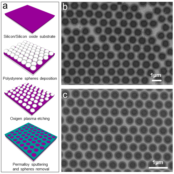
For the experimental verification of the memristance in nanostructured samples, we have developed Kagomé lattices by colloidal nanolithography. The process (summarized in Figure 1a) consists of transferring floating mono-layers of self-assembled (hexagonal closely packed) polystyrene spheres (PS), at air/water interface, to a thermally oxidized silicon substrate Burmeister ; Yi . Then, to increase the spacing between the PS spheres, the monolayers were developed by reactive ion etching with oxygen plasma for 12.5 minutes.
After this first step, a magnetic material deposition process was performed with Permalloy thin film capped by of platinum, deposited by sputtering over the set of substrate, plus PS spheres mask. Finally, the PS spheres were removed by deionized water ultrasonic bath to yield Kagomé lattices. Figure 1b and 1c shows scanning electron microscopy images of a representative lattice among the grew Kagomé lattices, using spheres with and diameter respectively.
II.2 Hysteretic Magnetoresistance
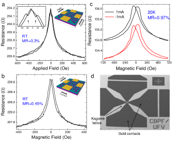
In order to perform electric and magnetoresistive characterization of our samples, electric contacts of gold 50nm, preceded by 3nm of chrome for better adhesion, were developed by sputtering in the geometries depicted in Figure 2.
To investigate the magnetoresistive behavior we have performed measurements in the longitudinal configuration (2a), with an angle of =0 between the applied current and sweep external magnetic field direction, and in the transverse configuration (2b) with =90. Our results on the magnetoresistive effect are in accordance with those present in literature amrsi . The anisotropic effect expected due to spin-orbit coupling in the Permalloy thin-film, highlighted in Figure 2a inset, is extremely suppressed by the dynamics of the vertex magnetization, which are responsible for the isotropic behavior observed in Figures 2a and 2b, performed at room temperature.
It is important to point out that the colloidal nanolithography we utilized has allowed an increase in the vertex size, in comparison with the nanowires width. As a result, the magnetoresistive effect we measured is approximately two orders of magnitude bigger than the ones observed in electron beam nanolithography samples of previous experiments amrsi . Moreover, we observed in the magnetoresistive curves an even more pronounced signal in the measurements performed at K, as presented in Figure 2c. It was also observed an hysteresis asymmetries in the curve shape for positive and negative external fields, depending on the current signal, and in the resistance for positive and negative applied currents. This suggests that there is both the AMR effect and a pinched hysteresis in the resistivity, providing evidence a memory effect as previously predicted amrsi ; cargwcnis .
II.3 Memristance
To test whether the resistive memory is memristive in nature, we have performed a typical memristor experiment, in which we have checked if responding to a sinusoidal voltage input one observes a pinched hysteresis. The results obtained are presented in Fig. 3. Specifically, we have performed curves to investigate the resistive memory effect in our samples with currents up to , applied in samples at room temperature and at .
The results presented in Figure 3a, both for a continuous Permalloy thin film and Kagomé lattice of diameter spheres performed at room temperature and T=20K, clearly show the memristive phenomenon characterized by the typical pinched loop in the curve plot. Such effect increases as temperature decreases, following the same behavior observed in the magnetoresistive curves. In the continuous Permalloy thin film, one can see that resistance is very low in comparison with Kagomé sample and just a very short loop in measurement is observed, in comparison with nanowired samples (Kagomé) (3a inset).
In order to check whether the memristive hysteresis is a function of the frequency and of the external applied magnetic field, we have performed curves at different frequencies under and without external magnetic field. As we show in Fig. 3b, the memory effect is higher for lower frequencies, while the slight difference as a function of the external field (3c) increases as the frequency decreases. This is typical of memristive behavior.
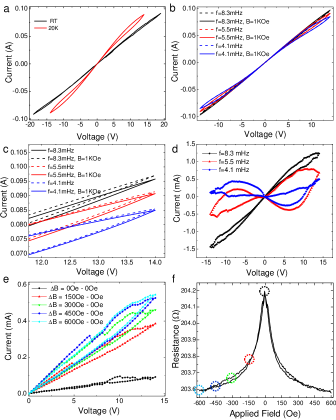
In all the measurements performed with and without an external field, the predicted resistive hysteresis was present. We noticed however memristive signals up to 13%, much larger than the expected from the analysis of amrsi , which considers just effects coming from many body magnetization flips, that should be in the same magnitude of sample AMR 1%.
In Figure 3d we plot instead the difference between the hysteresis curves, when the samples are submitted to a field strong enough to saturate the nanowires and vertices magnetization, for the different frequencies measured. Such plot is carried out in order to remove the part of signal probably coming from thermal effects, which also contribute to possible contributions coming from magnetization dynamics, leaving just the many body contribution. After the subtraction of the two curves obtained with and without magnetization saturation by external field, the characteristic pinched hysteresis loop is observed, now with the same magnitude of 1%. In Figure 3e we present similar curves for the measurements performed under intermediate fields. A very small cycle-to-cycle variation is observed (black curve), while under successive applied field memristive effect is increased up to saturation around . The proportionality of the memristive signal with the resistive change under external field can be noticed in the magnetoresistive curve presented in 3f.
II.4 Thermocouple analysis
Because of the disparity between the AMR measurement and the observed resistance change, the bulk of the memristive effect has to be found elsewhere. It was already demonstrated in literature that persistent high currents needed to move the domain walls in such Permalloy nanowires, in same order of x utilized in the present work, could be able to increase the temperature up to yamaguchi in nanowires with similar geometries to those utilized in our samples. Such temperatures could be high enough to stimulate thermal fluctuations of magnetization renan .
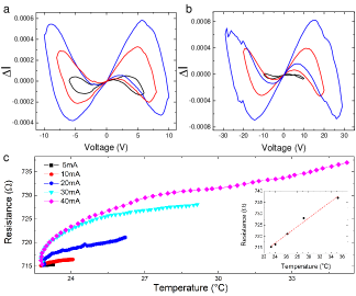
An insight of thermal effects relevance in the high memristive signal measured can be obtained from the measurements performed in samples with different nanowire lengths presented in Figure 4. The resistance measured in a sample obtained with diameter spheres (4 a) is half of sample resistance obtained with spheres (4 b), which presents higher memristive effects with same applied current of .
To map the evolution of resistance in function of sample heating by Joule effect, we have applied different persistent currents and measured the evolution of sample temperature with a K-type thermocouple for , timescale similar to the utilized for the curves. Results presented in (4 c) show linear evolution of resistance of around per Celsius degree.
The difference between the curves of Fig. 4 (c), and the hysteretic AMR analysis previously discussed, show that a temperature-based memristor model alone cannot explain all the effects in the material.
III Theoretical analysis of temperature contributions
III.1 Thermistor effect in heterostructures
While the splitting of the AMR experiment confirms a spin transfer torque effect, at the Hertz frequency we still have an effect of the temperature on the resistivity, causing a memristive hysteresis thermistor . It is worth here to characterize the properties of this thermistor in our samples. Let us assume that the resistivity of the material changes with the temperature, and that moreover we are in the regime of a thermistor. We thus ignore for the moment the AMR effect, e.g. a temperature dependent resistor with conductance . We want to show here that such effect is important because of the nanopatterning, which is consistent with the experimental results, due to the difference in area between a thin film and an heterostructure.
In order to explain this effect we used a thermistor model thermistor for the material. This is given by
| (2) | |||||
| (3) | |||||
| (4) |
where is room temperature, and for permalloy we have . The parameter physically represents the internal temperature of the permalloy. The parameter is fit to be approximately for our device at room temperature. The parameter seconds and represents the thermalization time of the sample at room temperature.
Then, Ohm’s law for the effective resistance of the sample follows
| (5) |
The sample can dissipate energy both through the silicon substrate and via radiative transfer. If is the conduction per unit of area, the Stefan-Boltzmann constant, and the heat capacity of the material, we have
and thus we obtain an effective memristive effect.
In order to estimate the frequency at which the thermistor effect is negligible, we use the the equation above. The estimate is independent from many body effects, and since the effective resistance of the sample depends on the resistivity linearly (while not on the topology) we can work with an effective model. The specific heat capacity of permalloy is cal/g/Celsius, the density . Also, it has been known for some time soviets that the electrical resistivity of permalloy is linear in temperature in the range Celsius, and nearly doubles in that interval (80% gain in resistivity). However, we are not aware of resistivity measurements for structures like ours. Given a certain initial condition, , thermocouple experiments are consistent with a negative coefficient thermistor, which follows an equation
| (7) |
with The total heat capacity can be written as , where is the density of the sample, and is the volume, given by the area times the thickness.
In our experiment we can have estimated that at , and at , from which we can estimate . Also, we neglect the radiative transport, since it is orders of magnitude smaller than the dissipation due to transfer of energy via the plate.
In order to make the equation adimensional, we divide by the room temperature energy, . If we define
| (8) |
we can write
and writing explicitly and in terms of the area and the resistance explicitly, we obtain
| (10) | |||||
and where we used
| (11) |
with ; thus, if we choose to be room temperature, then . For practical purposes, we can set . Now, we note that is a relaxation timescale, while is an effective activation voltage per unit of time, which depends on the area of the permalloy sample in contact with the surface. This implies that the smaller the area the more pronounced the memristive effect due to the temperature will be. This is one of the reasons why this effect is typically negligible in thin films, while it is more pronounced in our sample. Let us assume that the thermistor is near the equilibrium. What we are interested in is the interplay between the decay and the forcing and the relationship in terms of . We thus neglect the dependence on the denominator of the voltage-forcing term.
The solution of the differential equation in this regime, and assuming that is given by
where is constant of integration given the initial condition, which however we see goes to zero exponentially fast. As a result, from the oscillations around equilibrium, we can estimate in a linear response framework the value of . Since in our experiments we do not see a strong decay or thermalization, we expect to be of order seconds. Let us thus assume first that . In this case, we have
| (13) |
Since we observe that the oscillations in resistance are of order , we obtain a rough estimate for in the mhz of at . We thus have
| (14) |
Substituting these, we have
| (15) |
which, setting as a unit of time, leads to an effective voltage necessarily to observe a noticeable response in the frequency regime of our experiments of Volts. This is indeed consistent with the experimental results.
In the regime, , we have, up to the first order in
from which we see that while the equilibrium depends on , the oscillations do not. We obtain
| (16) |
The result above means that if we increase the frequency by , these should be suppressed by a factor . This argument suggest that if we observe a memristive effect in the or due the thermal changes, these should be suppressed by a factor in the Ghz, and thus negligible.
As a last comment, we now discuss why in thin films this effect is not usually observed, as we also found out in our experiments. The surface of the sample is roughly 25 , or . We have prepared two samples, one with sphere of and diameter. In the sample, we can perform the calculation by directly assuming a certain density of holes. In an area of we have roughly 110 spheres, give or take. This implies that we have itched out from the surface an area , and thus we obtain a remaining area . The ratio between . This implies that the ratio between the effective activation voltage per unit of second of the thin film is given by
| (17) |
or . The effect is thus at least one of magnitude smaller in a thin film permalloy, which implies voltages of at least Volts to fully appreciate the memory effect, which is prohibitive without burning the sample.
In conclusion of the model above, we obtained that the thermistor controlled at a certain frequency has two regimes for the change of resistance per unit of time (second):
-
•
: the time evolution of the system leads to a oscillatory regime around the mean, with
-
•
: a solution of the dynamics leads to a change in amplitude, given by
Again, since in our experiments we do not observe a strong decay or relaxation, we expect the relaxation time to be of the order of the seconds. We are thus in the first of the two regimes, which is what we use to estimate , which is approximately of . Thus, we obtain the result that at slow frequencies the system is dominated by thermal effects. This is one of the reasons which explains why in our experiments we do have little dependence of the hysteresis curve on an applied field. Yet, as we show above, for larger frequencies resistance memory oscillations are suppressed by a factor . This implies that at higher frequencies we have a crossover effect between the thermal and the magnetic degrees of freedom in the material, which we characterize next.
III.2 Magnetization dynamics
In a previous work it was argued that when a current is run through the Kagomé permalloy, the total resistance is finely controlled by the direction of magnetization of the wires amrsi ; amr ; gwc . It was shown gwc that the effect of the magnetoresistance is due to the presence of the vertices, where domain walls form, and the system can thus be interpreted as an electrical circuit with voltage drops at the vertices. In cargwcnis it has been noted instead that such construction can be mapped to a resistor network with voltage generators in series, and thus can be written in an analytical form and mapped to an effective memristive effect.
More recently, it has been shown that in magnetic nanorings, the interplay between AMR and the Zhang-Li coupling are sufficient for the ring to exhibit memristive effects which are strongly dependent on the internal magnetization states caravellimem . As we have seen here, magnetic permalloy patterned as Kagomé lattice shows a residual memristive effect (on top of the bulk thermistor effect) which is magnetic in nature. We wish to show here that such effect can in principle be attributed to a many body phenomenon which we attempt to qualitatively account for here.
As discussed in cargwcnis , for heterostructures such as a Kagomé patterned permalloy, the interplay between the AMR and the local magnetization of the structure can affect the resistivity of the material. Here we go beyond the spin-like approximation used in cargwcnis and study the magnetization reversal in a realistic model. Specifically, magnetization reversal processes in Kagomé nanowires were verified by micromagnetic simulations based on the open-source GPU-based software .
From energy minimization, one obtains sequences of snapshots between spin configurations, which are based on the Landau-Lifshitz-Gilbert (LLG) equation with the spin-transfer torque,
| (18) |
In simulations we have used periodic boundary conditions on a lattice of m m size and with finite difference discretization for the iterations (following Eq. (18) with cubic cell of nm nm nm). The numerical parameters we used were those of permalloy, for which later in this letter we performed the experiments. They were magnetic saturation A m-1, exchange constant J m-1, polarization and Gilbert damping for dynamics. In simulations we introduced a density of current A/ m2, cycling at a frequency . The numerical calculations were carried by a second-order Heun’s solver with a fixed time step of Leliaert .
To better understand the role of magnetization dynamics in the memristive effect in the measurements performed in kagomé lattices, while an analysis of extended magnetic objects escapes a complete analytical treatment, the intuition for the behavior of electrical-magnetic interactions can be obtained via intense numerical scrutiny. For that purpose we have utilized micromagnetic simulations in samples without (5a) and with (5b) the presence of an applied 0.3T constant magnetic field on the y-axys.
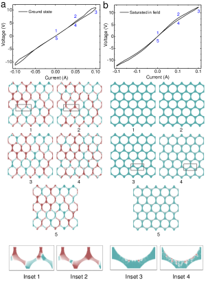
In the frames of magnetization distribution taken in positions 1-5 during the current loop, one can see that in the lattice without external magnetic field two processes are present, domains wall motion by the current, which is applied in the y-direction, with nanowires magnetization flip in the x-direction (inset 1 and 2), aside of periodic domain wall creation and annihilation by the particular geometry of the borders for high currentssitte .
Despite the many-body effect contribution to the memristive effect, analytically predicted in previous work amrsi , the asymmetric disorder brought by the periodic domain wall creation between increasing (frame 2) and decreasing (frame 4) current regime is mainly responsible for the memristive effect observed. In the saturated regime under an external magnetic field, the many-body effect is not present as expected, however, the geometric anisotropy is strong enough to shift the magnetization in relation to the current polarization direction to achieve the condition for periodic domain wall creation, then even in saturation regime, the asymmetric disorder is observed (insets 3 and 4).
IV Conclusion
The present paper is the first experimental investigation of the AMR-induced memristive effect in magnetic materials.
We have lithographically printed (via colloidal deposition) a Kagomé lattice of permalloy nanowires with two different lengths, and studied the device memristive phenomenology in comparison with the thin film. The history dependence of the magnetization on the current has been observed in the analysis of the anisotropic magnetoresistance, which has a higher signal in comparison with e-beam lithographed samples, due to the large area of vertex obtained. While the bulk of the phenomenon can be explained via a thermistive effect not present in thin films, also confirmed via a thermocouple analysis, we have found that 1% of the effect can be associated to the AMR induced hysteresis.
In order to characterize the phenomenon, we have studied via micromagnetic simulations the effect of the current in the sample, and found that domain walls and spin waves can be found. However, thermal and dynamicals effects could be removed by analyzing the difference between curves obtained in the experiments with and without external fields, and the many body memristive characteristic could be measured.
While overall we do find that a residual effect can be attributed to a magnetic-induced memristive effect, both in numerical simulations and experiments, the presence of the contribution of a thermistive effect prevents us for making precise statements on the nature of the phenomenon. This said, we do find good evidence that the combination of a coupling between the magnetization and the current via spin-torque and anisotropic magneto-resistance leads to a polar memristive effect. Some comments are in order. It is interesting to note that the hysteresis curves of our experiments exhibit very little noise levels compared to other similar devices.ProbComp5 This is typically not the case for memristors, which have (again, typically) noise in the hysteresis curve.
Our numerical results and experiments suggest that tuning parameters, and using different materials, could allow domain wall motion at lower currents. The theoretical analysis we performed on the thermistor also suggest that the thermistive effect should not be present at higher frequencies. Thus, experiments performed in the Ghz regime should eliminate spurious effects. Similarly to what described for the case of magnetic rings caravellimem , pure magnetically induced memristive effects should be present at that scale.
V Acknowledgements.
The financial support for this research was provided by the Brazilian agencies FINEP, FAPEMIG, and CAPES (Finance Code 001). The work of FC was carried out under the auspices of the US Department of Energy through the Los Alamos National Laboratory, operated by Triad National Security, LLC (Contract No. 892333218NCA000001).
Author contributions
W.B.J.F and F.G. designed and developed the samples. C.I.L.A performed the experimental measurements and numerical simulations and F.C worked on the theoretical model. All authors contributed to discussing the experiments, the models to explain it and writing the paper.
References
- (1) C. Castelnovo, R. Moessner, and S. L. Sonhdi, Spin ice, fractionalization, and topological order, Annu. Rev. Condens. Matter Phys. 3, 35-55 (2012).
- (2) E. Mengotti et al., Real-space observation of emergent magnetic monopoles and associated Dirac strings in artificial Kagomé spin ice, Nat. Phys. 7, 68-74 (2010).
- (3) Y. Lao et al., Classical topological order in the kinetics of artificial spin ice, Nature Phys. 14, 723-727 (2018).
- (4) G.-W. Chern, P. Mellado, Magnetic monopole polarons in artificial spin ices, Europhys. Lett. 114, 37004 (2016).
- (5) S. Gliga, et al., Spectral analysis of topological defects in an artificial spin-ice lattice, Phys. Rev. Lett. 110, 117205 (2013).
- (6) C. Nisoli, R. Moessner, and P. Schiffer, Colloquium: Artificial spin ice: Designing and imaging magnetic frustration, Rev. Mod. Phys. 85, 1473 (2013)
- (7) R. F. Wang et al., Artificial spin ice in a geometrically frustrated lattice of nanoscale ferromagnetic islands, Nature 439, 303-6, (2006).
- (8) S.D. Bader, Colloquium: Opportunities in nanomagnetism, Rev. Mod. Phys. 78, 1, (2006).
- (9) I. Gilbert et al., Emergent reduced dimensionality by vertex frustration in artificial spin ice, Nature Phys. 12, 162-165 (2016).
- (10) L. J. Heyderman, R. L. Stamps, Artificial ferroic systems: novel functionality from structure, interactions and dynamics, J. Phys.: Conden. Matter 25, 363201 (2013).
- (11) B. Canals et al., Fragmentation of magnetism in artificial Kagomé dipolar spin ice, Nat. Comm. 7, 11446 (2016).
- (12) I. A. Chioar, N. Rougemaille, and B. Canals, Ground-state candidate for the classical dipolar Kagomé Ising antiferromagnet, Phys. Rev. B 93, 214410 (2016).
- (13) C. Nisoli, R. Wang, J. Li, W. F. McConville, P. E. Lammert, P. Schiffer, and V. H. Crespi, Ground State Lost but Degeneracy Found: The Effective Thermodynamics of Artificial Spin Ice, Phys. Rev. Lett. 98, 217203 (2007).
- (14) C. Nisoli, J. Li, X. Ke, D. Garand, P. Schiffer, and V. H. Crespi, Effective Temperature in an Interacting Vertex System: Theory and Experiment on Artificial Spin Ice, Phys. Rev. Lett. 105, 047205 (2010).
- (15) I. Gilbert et al., Direct visualization of memory effects in artificial spin ice. Phys. Rev. B, 92, 104417 (2015).
- (16) P. E. Lammert et al., Direct entropy determination and application to artificial spin ice. Nat. Phys. 6, 786-789 (2010).
- (17) F. Caravelli, C. Nisoli, Computation via Interacting Magnetic Memory Bites: Integration of Boolean Gates, New Journal of Physics (2020), arXiv:1810.09190.
- (18) H. Arava et al., Computational logic with square rings of nanomagnets, Nanotechnology 29, no. 26 265205 (2018).
- (19) J. H. Hensen, E. Folven, G. Tufte, Computation in artificial spin ice, Proc. of ALIFE 2018, pp. 15-22, MIT Press, 10.1162/isal-a-00011 (2018)
- (20) S. A. Wolf et al., Spintronics: A Spin-Based Electronics Vision for the Future, Science 294 1488-1495 (2001)
- (21) A. Ney et al., Programmable computing with a single magnetoresistive element” Nature 425 485-7 (2003).
- (22) H. Dery et al., “Spin-based logic in semiconductors for reconfigurable large-scale circuits”, Nature 447(7144):573-6 (2007)
- (23) M. Patra, S. K. Maiti, All-spin logic operations: Memory device and reconfigurable computing, Europhys. Lett. 121, 38004 (2018).
- (24) Y. Zhang, IEEE in Design, Automation and Test in Europe Conference and Exhibition, 10.7873/DATE.2014.316 (2014)
- (25) F. L. Traversa et al., Memcomputing NP-complete problems in polynomial time using polynomial resources and collective states, Science Advances 1, e1500031 (2015).
- (26) F. L. Traversa, M. Di Ventra, Polynomial-time solution of prime factorization and NP-complete problems with digital memcomputing machines, Chaos 27, 023107 (2017).
- (27) H. Manukian et al., Memcomputing Numerical Inversion With Self-Organizing Logic Gates, IEEE Trans Neural Netw Learn Syst. 29, 2645 (2017).
- (28) F. Traversa, M. Di Ventra, Memcomputing: Leveraging memory and physics to compute efficiently, J. App. Phys. 123, 180901 (2018).
- (29) F. Caravelli, F. L. Traversa, M. Di Ventra, Complex dynamics of memristive circuits: Analytical results and universal slow relaxation”, Phys. Rev. E 95, 022140 (2017).
- (30) F. Caravelli, Asymptotic behavior of memristive circuits and combinatorial optimization, Entropy 21, 789 (2019).
- (31) F. Caravelli, J. P. Carbajal, Memristors for the curious outsiders, Memristors for the curious outsiders, Technologies, 6, 118 (2018); engrXiv preprint:c4qr9.
- (32) D. S. Jeong et al., Memristors for Energy‐Efficient New Computing Paradigms, Adv. Electron. Mater., 2, 1600090 (2016).
- (33) T. Serrano-Gotarredona et al., Front. Neurosci. 7: 2 (2013) https://doi.org/10.3389/fnins.2013.00002
- (34) B. Le, J. Park, J. Sklenar, G.-W. Chern, C. Nisoli, J. Watts, M. Manno, D. Rench, N. Samarth, C. Leighton, P. Schiffer, Understanding magnetotransport signatures in networks of connected permalloy nanowires, Phys. Rev. B 95, 060405(R) (2017).
- (35) T. R. McGuire and R. I. Potter, Anisotropic magnetoresistance in ferromagnetic 3d alloys, IEEE Trans. Magnetics 11, 1018 (1975).
- (36) W. R. Branford, S. Ladak1, D. E. Read1,2, K. Zeissler1, L. F. Cohen, Emerging Chirality in Artificial Spin Ice, Science 335, 1597-1600 (2012).
- (37) G.-W. Chern, Magnetotransport in artificial Kagomé spin ice, Phys. Rev. Applied 8, 064006 (2017).
- (38) F. Caravelli, G.-W. Chern, C. Nisoli, Artificial Spin Ice Phase-Change Memory Resistors, New Journal of Physics, https://doi.org/10.1088/1367-2630/ac4c0a (2022)
- (39) F. Caravelli, E. Iacocca, G.-W. Chern, C. Nisoli, C. I. L. de Araujo, Anisotropic MagnetoMemristance, arXiv:2109.05101
- (40) F. Burmeister et al., Colloid monolayers as versatile lithographic masks, Langmuir 13, 2983-2987 (1997).
- (41) Z. Yi et al., Ordered array of Ag semishells on different diameter monolayer polystyrene colloidal crystals: An ultrasensitive and reproducible SERS substrate, Sci. Rep. 6, 32314 (2016).
- (42) D.B. Strukov, G. Snider, D.R. Stewart, and R.S. Williams, The missing memristor found, Nature 453, pp. 80-83 (2008)
- (43) S. Zhang, Z. Li, Roles of Nonequilibrium Conduction Electrons on the Magnetization Dynamics of Ferromagnets, Phys. Rev. Lett. 93, 127204 (2004)
- (44) A. Yamaguchi et al., Real-Space Observation of Current-Driven Domain Wall Motion in Submicron Magnetic Wires, Phys. Rev. Lett. 92, 077205 (2004).
- (45) S. Krishnia, I. Purnama, W. S. Lew, Observation of ice-rule violation and monopole dynamics via edge nucleation of domain walls in artificial spin ice lattice, J. Mag. Mag. Materials 420, 158-165 (2016).
- (46) N. Vernier et al., Domain wall propagation in magnetic nanowires by spin-polarized current injection, Europhys. Lett. 65 526 (2004).
- (47) A. Pushp et al., Domain wall trajectory determined by its fractional topological edge defects, Nature Phys. 9, 505-511 (2013).
- (48) L.D. Landau, E.M. Lifshitz, Theory of the dispersion of magnetic permeability in ferromagnetic bodies, Phys. Z. Sowjetunion. 8, 153. (1935)
- (49) T.L. Gilbert, ”A Lagrangian formulation of the gyromagnetic equation of the magnetic field”, Phys. Rev. 100 (4): 1243 (1955)
- (50) JM. Ginoux, et al. A physical memristor based Muthuswamy–Chua–Ginoux system. Sci Rep 10, 19206 (2020)
- (51) Y. Qi, T. Brintlinger, J. Cumings, Direct observation of the ice rule in an artificial Kagomé spin ice, Phys. Rev. B 77, 094418 (2008).
- (52) S. Zhang et al. Crystallites of magnetic charges in artificial spin ice, Nature 500, 553-557 (2013).
- (53) B. Bollobas, Modern Graph Theory, Springer Science, New York (1998)
- (54) F. Caravelli, “Locality of interactions in memristive circuits”, Phys. Rev. E 96, 052206 (2017).
- (55) F. Caravelli, “The mise en scéne of memristive networks: effective memory, dynamics and learning”, Int. J. of Par., Em. and Dist. Sys., 33, 350-366, (2018)
- (56) G.-W. Chern, O. Tchernyshyov, “Magnetic charge and ordering in Kagomé spin ice”, Phil. Trans. Roy. Soc. A 370, 5718 (2012)
- (57) N. Locatelli, V. Cros, J. Grollier, Nature Materials, 13, 11 (2014).
- (58) S. Raoux, F. Xiong , M. Wuttig, E. Pop, MRS Bulletin 39, pp. 703-710 (2014).
- (59) M. Stiles, J. Miltat, B. Hillebrands, A. Thiaville (Eds.): Spin Dynamics in Confined Magnetic Structures III, Topics Appl. Physics 101, 225–308 (2006) (Springer-Verlag Berlin Heidelberg 2006)
- (60) R. P. Loreto et al., Experimental and theoretical evidences for the ice regime in planar artificial spin ices. Journal of Physics: Condensed Matter, v. 31, n. 2, p. 025301, (2018).
- (61) A. Yamaguchi et al., Effect of Joule heating in current-driven domain wall motion. Applied Physics Letters, v. 86, n. 1, p. 012511, (2005).
- (62) I. R. B. Ribeiro et al., Investigation of ferromagnetic resonance and magnetoresistance in anti-spin ice structures. Journal of Physics: Condensed Matter, v. 28, n. 45, p. 456002, (2016).
- (63) J. Leliaert et al., AIP Adv. 7(12), 125010 (2017).
- (64) M. Sitte et al., ”Current-driven periodic domain wall creation in ferromagnetic nanowires.” Physical Review B 94.6 064422 (2016).
- (65) A. D. Avery, S. J. Mason, D. Bassett, D. Wesenberg, and B. L. Zink, “Thermal and electrical conductivity of approximately 100-nm permalloy, Ni, Co, Al, and Cu films and examination of the Wiedemann-Franz Law”, Phys. Rev. B 92, 214410 (2015)
- (66) E. Iacocca, T. J. Silva, M. A. Hoefer, Breaking of Galilean Invariance in the Hydrodynamic Formulation of Ferromagnetic Thin Films, Phys. Rev. Lett. 118, 017203 (2017)
- (67) Belous, M. V., Permyakov, V. G., Popov, V. I. (1967). The electrical properties of thin permalloy films. Soviet Physics Journal, 10(3), 23–24.