Large Andreev Bound State Zero Bias Peaks in a Weakly Dissipative Environment
Abstract
We study Andreev bound states in hybrid InAs-Al nanowire devices. The energy of these states can be tuned to zero by gate voltage or magnetic field, revealing large zero bias peaks (ZBPs) near in tunneling conductance. Probing these large ZBPs using a weakly dissipative lead reveals non-Fermi liquid temperature () dependence due to environmental Coulomb blockade (ECB), an interaction effect from the lead acting on the nanowire junction. By increasing , these large ZBPs either show a height increase or a transition from split peaks to a ZBP, both deviate significantly from non-dissipative devices where a Fermi-liquid dependence is revealed. Our result demonstrates the competing effect between ECB and thermal broadening on Andreev bound states.
Andreev bound states (ABSs) can emerge in non-uniform superconductors by Andreev scattering at energies below the superconducting gap [1, 2]. Hybrid semiconductor-superconductor systems [3, 4, 5, 6] provide an ideal test-bed to study these subgap states, thanks to the proximity effect mediated by Andreev reflections and the high tunability of carrier density using electrostatic gates. Fascinating physics can be revealed by adding additional elements, e.g. one dimensionality and spin-oribt coupling [7, 8, 9, 10, 11, 12]. These hybrid nanowires, with the semiconductor being InAs or InSb, are further predicted to host Majorana zero modes (MZMs) [13, 14] where one ABS can be spatially separated into two ‘halves’ (MZMs). In tunneling conductance, zero bias peaks (ZBPs) can be observed [15, 8, 16, 17, 18, 19, 20] as a possible signature for MZMs as well as zero-energy ABSs. The similarities between ABSs and MZMs create huge debates on distinguishing them [21, 22, 23, 24, 25, 26, 27, 28, 29, 30, 31, 32, 33].
Recently, motivated by a theoretical work [34], we have added a resistive lead as a strongly dissipative environment to the hybrid InAs-Al devices [35]. Previously, dissipative tunneling of metallic junctions [36, 37, 38, 39, 40] and semiconductor nanostructures [41, 42, 43, 44, 45, 46] have been widely studied, exhibiting environmental Coulomb blockade (ECB) with power laws emulating Luttinger liquid physics [47]. Here [35], the interaction effect in the environment acts on the InAs-Al nanowire junction where ABSs emerge. In the strongly dissipative regime, we have shown that most zero-energy ABSs are revealed as split peaks instead of ZBPs [35]. However, it still remains as an interesting question to ask how do ABS-induced ZBPs, if not being fully suppressed, behave in a dissipative environment. In this work, we lower the dissipation strength by reducing the lead resistance from 5.7 k in Ref. [35] to 2.7 k. In this weak dissipation regime, we can resolve large (trivial) ZBPs near , the main focus of the current debates [30, 31, 32]. dependence of these large ZBPs behave dramatically different from that of small ZBPs or ZBPs in regular devices without dissipation. We ascribe this difference to the dynamical competition between ECB and thermal averaging. Our result sets a lower bar on dissipation strength if being used to distinguish MZMs [34].
Fig. 1a shows the scanning electron micrograph (SEM) of Device A. An InAs nanowire (gray) with a thin Al shell (cyan) is first contacted by Ti/Au (yellow), and then connected to a resistive film (red), serving as the dissipative environment. Resistance of the dissipative film is designed and later estimated to be 2.7 k (see Fig. S1 for details). The device can be tuned by a side tunnel gate (TG) and a global back gate (BG) which is p-doped Si covered by 300 nm thick SiO2. Growth and transport details of these hybrid InAs-Al nanowires can be found in Ref. [48, 19]. We apply a total bias voltage () on the left Ti/Au lead, and measure the current from the right contact. The bias drop on the InAs-Al part is , where includes resistance of the fridge filters and the dissipative film, both estimated based on independent calibration. The device differential conductance has excluded.
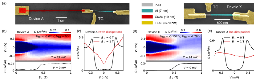
In Fig. 1b we tune the device into tunneling regime and resolve the superconducting gap (see Fig. S2 for a full gate scan). The gap is closed by a magnetic field (), perpendicular to the nanowire, at 0.5 T. After the gap closing, a dip is resolved near zero-bias (red curve in Fig. 1c). This suppression of near zero-bias (see Fig. S3 more scans) is a signature of ECB. We further quantify this suppression with power laws and find rough matches (see Fig. S4). The small deviations from power law fitting indicate an incomplete ECB suppression of imperfections, e.g. defects and local states in the InAs-Al junction. In our control Device X, an InAs-Al nanowire without the dissipative resistor, is usually flat after the gap closing without noticeable features near zero-bias as shown in Fig. 1de.
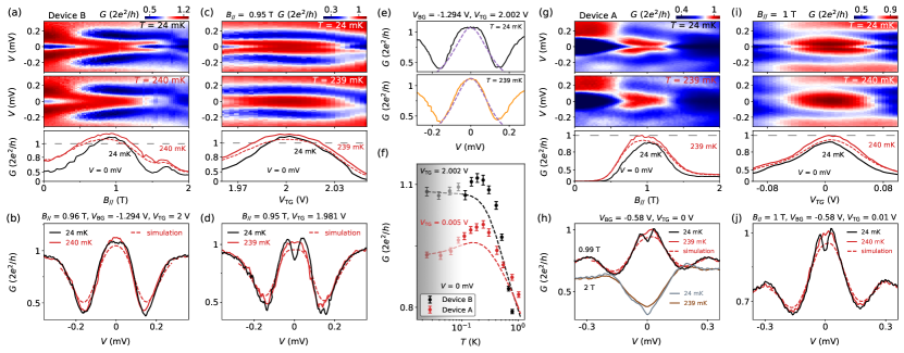
We now align parallel to the nanowire and find large ZBPs due to zero-energy ABSs. Fig. 2a shows a scan of an ABS, likely disorder-induced, in Device B at temperatures () of 24 mK and 240 mK. refers to the fridge unless specified. Device B has a dissipative resistor ( 2.7 k) similar to that in Device A. At 0.96 T, two peaks merge at zero and form a large ZBP with its height exceeding , see Fig. 2b line cuts. Interestingly, the ZBP height at an elevated of 240 mK (red curve) is higher than that at base of 24 mK (black). This unusual dependence is qualitatively different from those in non-dissipative devices where the ZBP height always decreases as increases, a purely thermal broadening (averaging) effect (see Fig. S5 examples in control Device X). We attribute this unusual dependence to the mixing or competing effect of ECB and thermal broadening. ECB suppresses zero-bias (the ZBP height) at low (24 mK). Higher (240 mK) diminishes ECB and enhances the height. On the contrary, thermal broadening, an averaging effect over a peak, leads to the opposite trend in dependence. For large and broad ZBPs, thermal broadening effect is not obvious at low , therefore ECB may dominate the trend in dependence, as visualized by the difference between the black and the red curves in Fig. 2b. Note that ECB is the strongest near zero .
To simulate the thermal broadening effect, we use the formula , where is the Fermi distribution function. at high can be calculated by this convolution using = 0 K as an input which we replace with = 24 mK. This assumption should be valid for much larger than 24 mK. The red dashed lines in Fig. 2a (lower panel) and Fig. 2b are the simulation results for = 240 mK, noticeably lower than the measured at the same (red lines). This deviation suggests that thermal broadening is not the only effect and ECB should be included in the dependence of large ZBPs.
Fig. 2c shows the gate dependence of the large ZBP where again a sizable deviation can be found between the measurement (red line) and the thermal simulation (dashed line) for = 239 mK. Fig. 2d shows a line cut of the near-zero-energy ABS: split peaks at 24 mK evolving into a large ZBP at 239 mK. The red dashed line is the thermal simulation which could also merge split peaks into a ZBP but at a cost of lowering the peak height.
ECB not only suppresses the ZBP height, but also modifies the peak shape due to its non-uniform suppression over bias. In Fig. 2e, the large ZBP at base shows larger deviation from the Lorentzian fit (dashed line) than that at higher . This phenomenon is expected since ECB is stronger (weaker) at lower (higher) . Fig. 2f shows the full dependence of the zero-bias (black dots) for this ZBP. The black dashed line is the thermal simulation which, as expected, shows a monotonic decrease with increasing . Contrarily, the measured ZBP height first increases (ECB being weakened) and then decreases until being too high where thermal broadening starts dominating. We sketch a gradient gray background for 100 mK indicating that below which the electron gradually deviates from the fridge and finally saturates.
Similar ZBPs near (with a smaller above-background-peak-height) can also be observed in Device A, as shown in Fig. 2g-j. Differently, this zero-energy ABS resolves a small splitting at base (black curves in Fig. 2hj). This splitting feature has no fundamental difference from the large (non-split) ZBP in Fig. 2b (black curve). Splitting or not depends on the zero-energy ABS details, dissipation strength and . If the electron in Fig. 2b could be further lowered towards zero, ECB would suppress more and the ZBP in Fig. 2b would also split. If the dissipation strength was increased towards the strong dissipation regime, most zero-energy ABS induced ZBPs would split. In fact, in Fig. 2a (for slightly different from 0.96 T) and Fig. 2d, we could also find large ZBPs at higher s which resolve a small splitting at base . Nevertheless, compared with Fig. 2b, Fig. 2h demonstrates a different regime for zero-energy ABS with a small splitting at base . The main noticeable difference between base (black curve) and higher (red curve) in Fig. 2hj is the ‘triangle’ area near zero-bias, a visualization of ECB (also visible for the 2 T line cuts). Note that thermal simulation (red dashed lines) conserves the area underneath the curve, making the peak height lower and peak width wider for higher s.
The red dots in Fig. 2f illustrate the evolution of the zero-bias corresponding to this zero-energy ABS. With increasing , the zero-bias first increases and then decreases, similar to the black dots. Though if using a split-peak at base as the input, thermal simulation would also give an initial increase of (purely due to averaging effect on a dip) as shown by the red dashed line. This increase is much less than the measurement data, indicating the noticeable role of ECB. For more dependence of the ABSs in Fig. 2, see Fig. S6.
Above we have demonstrated the interplay between weak dissipation (ECB) and thermal broadening on large ZBPs induced by zero-energy ABSs. These large ZBPs generally have a large peak width, therefore immune to thermal broadening for s being not too high (e.g. below 300 mK). Within this range, increasing diminishes ECB and enhances the zero-bias , causing deviations from the Fermi-liquid dependence (thermal simulation).
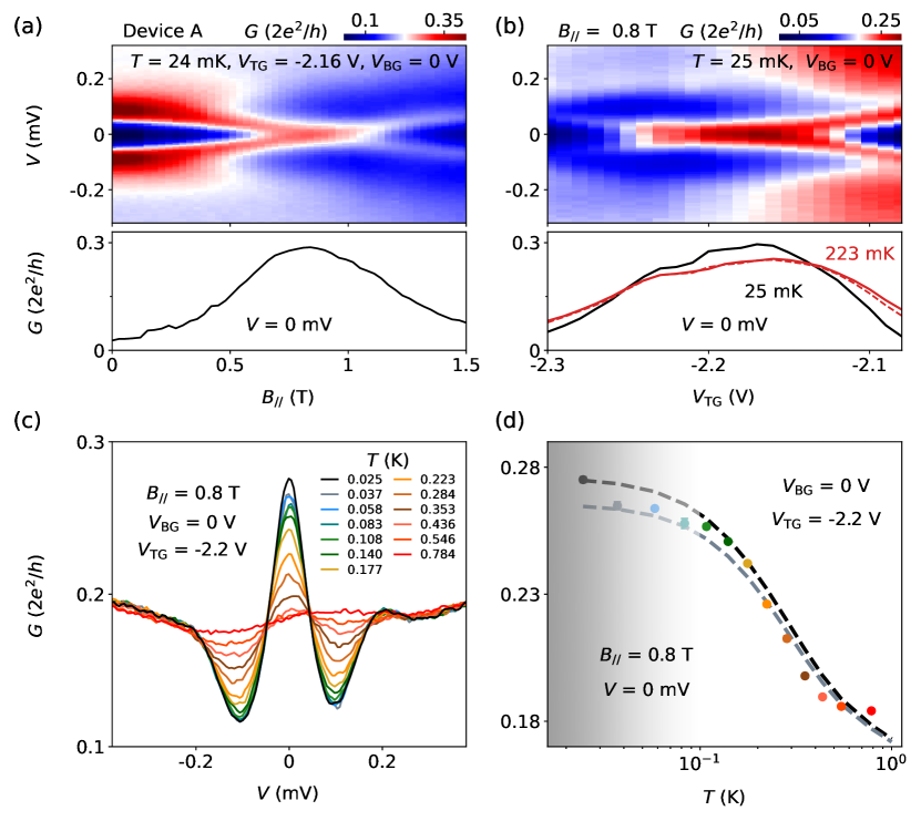
In Fig. 3 we study small ZBPs in Device A under the same dissipation strength. Fig. 3ab show the and gate scan of an ABS at base . The level crossing point, corresponding to a zero-energy ABS, resolves a small ZBP (peak height ). The ZBP width is also narrower than those in Fig. 2, therefore more sensitive to thermal averaging. Indeed, in Fig. 3b (lower panel), the thermal simulation (dashed line) for = 223 mK agrees reasonably well with the measurement (red line), suggesting that thermal broadening is the dominating effect, different from the large ZBP case in Fig. 2.
Fig. 3c and 3d show the full evolution of this small ZBP. The zero-bias (dots in Fig. 3d) shows a monotonic decrease as increasing , qualitatively different from the trend of dependence in Fig. 2. Moreover, thermal simulation (both black and gray dashed lines in Fig. 3d) matches reasonable well with the measurement, confirming thermal averaging as the dominating effect for small ZBPs. Note that weak dissipation should still be present for this ABS since they all share the same dissipative resistor. The narrower peak widths for small ZBPs make them more sensitive to thermal averaging. This causes ECB effect almost unnoticeable in the evolution. For more dependence and gate scans of this ABS, see Fig. S7. In Fig. S8, we present some stability tests of the ABSs in Fig. 2 and Fig. 3 to rule out possible gate shifts or charge jumps. Fig. S9-S11 show four more zero-energy ABSs with intermediate ZBP heights to illustrate the gradual transition from large to small ZBPs.
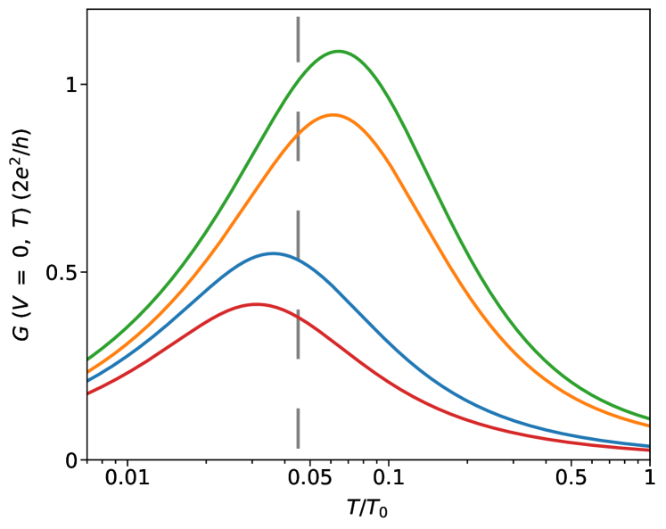
In Fig. 4, we present the result of renormalization group (RG) calculation for zero-energy ABSs by fixing the dissipation strength = 0.1. This translates to an effective dissipative resistance of 2.58 k, similar to the case of Device A and B. In the theory model [49], we could modify the lead-ABS tunnel couplings for electrons () and Andreev reflected holes () to realize different ZBP heights: if and are larger and closer, the ZBP height is larger. Fig. 4 demonstrates the dependence of zero-energy ABSs with different heights (colors). When decreases towards absolute zero, the zero-bias should be suppressed towards zero due to dissipation for all ABS cases, causing ZBP splitting. When is high enough and increases, ECB is diminished and the ZBP is thermally smeared, also causing the zero-bias to decrease. These two regions combined together form the shape of dependence in Fig. 4 with a maximum peak at an intermediate . The key point is that this intermediate is different for large and small ZBPs. By comparing with experimental data, we think our base likely corresponds the vertical dashed line. Under this assumption, for small ZBPs (the red and blue curves), the zero-bias shows a continuous decrease as increasing , consistent with the observation in Fig. 3. For large ZBPs (the orange and green curves), the zero-bias initially increases and then decreases as increasing , consistent with the observation in Fig. 2.
To summarize, we have studied zero-energy ABSs in a weakly dissipative environment. Large ZBPs near can be resolved. The large peak width protects the ZBP height from decreasing against thermal averaging over an intermediate -range (e.g. 300 mK) where ECB could dominate. As a result, when is lowered, the ZBP could either decrease its height or split, both not following Fermi-liquid thermal simulation. On the contrary, dependence of small ZBPs follows thermal simulation, same with the cases in regular devices without dissipation. Our result shows that weak dissipation strength ( 2.7 k) can not suppress ABS-induced ZBPs, therefore sets a lower bar on dissipation strength for future MZM devices [50]. For Majorana or quasi-Majorana resonance detection [25, 26], stronger dissipation regime [35] is preferred which can effectively ‘filter out’ trivial ZBPs [34, 51, 52, 49]. Since in the weak dissipation regime, the heights of ZBPs induced by zero-energy ABSs could either increase (Fig. 2) or decrease (Fig. 3) as increasing , depending on the ABS details. This makes it difficult to distinguish MZM signatures [53, 54] solely based on the dependence [34].
Acknowledgment Raw data and processing codes within this paper are available at https://doi.org/10.5281/zenodo.6123849. This work is supported by Tsinghua University Initiative Scientific Research Program, Alibaba Innovative Research Program, National Natural Science Foundation of China (Grant No. 92065106, 61974138, 11974198, and 12004040), Beijing Natural Science Foundation (Grant No. 1192017). D. P. acknowledges the support from Youth Innovation Promotion Association, Chinese Academy of Sciences (No. 2017156).
References
- Andreev [1965] A. Andreev, Thermal conductivity of the intermediate state of superconductors ii, Sov. Phys. JETP 20, 1490 (1965).
- Andreev [1966] A. Andreev, Electron spectrum of the intermediate state of superconductors, Sov. Phys. JETP 22, 18 (1966).
- Pillet et al. [2010] J. Pillet, C. Quay, P. Morfin, C. Bena, A. L. Yeyati, and P. Joyez, Andreev bound states in supercurrent-carrying carbon nanotubes revealed, Nature Physics 6, 965 (2010).
- Dirks et al. [2011] T. Dirks, T. L. Hughes, S. Lal, B. Uchoa, Y.-F. Chen, C. Chialvo, P. M. Goldbart, and N. Mason, Transport through andreev bound states in a graphene quantum dot, Nature Physics 7, 386 (2011).
- Chang et al. [2013] W. Chang, V. Manucharyan, T. Jespersen, J. Nygård, and C. Marcus, Tunneling spectroscopy of quasiparticle bound states in a spinful josephson junction, Physical Review Letters 110, 217005 (2013).
- Jiang et al. [2021] Y. Jiang, S. Yang, L. Li, W. Song, W. Miao, B. Tong, Z. Geng, Y. Gao, R. Li, Q. Zhang, et al., Selective area epitaxy of pbte-pb hybrid nanowires on a lattice-matched substrate, arXiv preprint arXiv:2110.13642 (2021).
- van Dam et al. [2006] J. A. van Dam, Y. V. Nazarov, E. P. Bakkers, S. De Franceschi, and L. P. Kouwenhoven, Supercurrent reversal in quantum dots, Nature 442, 667 (2006).
- Lee et al. [2014] E. J. Lee, X. Jiang, M. Houzet, R. Aguado, C. M. Lieber, and S. De Franceschi, Spin-resolved andreev levels and parity crossings in hybrid superconductor–semiconductor nanostructures, Nature Nanotechnology 9, 79 (2014).
- Zhang et al. [2017] H. Zhang, Ö. Gül, S. Conesa-Boj, M. P. Nowak, M. Wimmer, K. Zuo, V. Mourik, F. K. De Vries, J. Van Veen, M. W. De Moor, et al., Ballistic superconductivity in semiconductor nanowires, Nature Communications 8, 1 (2017).
- de Moor et al. [2018] M. W. de Moor, J. D. Bommer, D. Xu, G. W. Winkler, A. E. Antipov, A. Bargerbos, G. Wang, N. Van Loo, R. L. O. het Veld, S. Gazibegovic, et al., Electric field tunable superconductor-semiconductor coupling in majorana nanowires, New Journal of Physics 20, 103049 (2018).
- Bommer et al. [2019] J. D. Bommer, H. Zhang, Ö. Gül, B. Nijholt, M. Wimmer, F. N. Rybakov, J. Garaud, D. Rodic, E. Babaev, M. Troyer, et al., Spin-orbit protection of induced superconductivity in majorana nanowires, Physical Review Letters 122, 187702 (2019).
- Jünger et al. [2020] C. Jünger, R. Delagrange, D. Chevallier, S. Lehmann, K. A. Dick, C. Thelander, J. Klinovaja, D. Loss, A. Baumgartner, and C. Schönenberger, Magnetic-field-independent subgap states in hybrid rashba nanowires, Physical Review Letters 125, 017701 (2020).
- Lutchyn et al. [2010] R. M. Lutchyn, J. D. Sau, and S. Das Sarma, Majorana fermions and a topological phase transition in semiconductor-superconductor heterostructures, Phys. Rev. Lett. 105, 077001 (2010).
- Oreg et al. [2010] Y. Oreg, G. Refael, and F. von Oppen, Helical liquids and majorana bound states in quantum wires, Phys. Rev. Lett. 105, 177002 (2010).
- Mourik et al. [2012] V. Mourik, K. Zuo, S. M. Frolov, S. Plissard, E. P. Bakkers, and L. P. Kouwenhoven, Signatures of majorana fermions in hybrid superconductor-semiconductor nanowire devices, Science 336, 1003 (2012).
- Deng et al. [2016] M. Deng, S. Vaitiekėnas, E. B. Hansen, J. Danon, M. Leijnse, K. Flensberg, J. Nygård, P. Krogstrup, and C. M. Marcus, Majorana bound state in a coupled quantum-dot hybrid-nanowire system, Science 354, 1557 (2016).
- Gül et al. [2018] Ö. Gül, H. Zhang, J. D. Bommer, M. W. de Moor, D. Car, S. R. Plissard, E. P. Bakkers, A. Geresdi, K. Watanabe, T. Taniguchi, et al., Ballistic majorana nanowire devices, Nature Nanotechnology 13, 192 (2018).
- Zhang et al. [2021] H. Zhang, M. W. de Moor, J. D. Bommer, D. Xu, G. Wang, N. van Loo, C.-X. Liu, S. Gazibegovic, J. A. Logan, D. Car, R. L. M. Op het Veld, P. J. van Veldhoven, S. Koellinga, M. A. Verheijen, M. Pendharkar, D. J. Pennachio, B. Shojaei, J. S. Lee, C. J. Palmstrøm, E. P. Bakkers, S. Das Sarma, and L. P. Kouwenhoven, Large zero-bias peaks in insb-al hybrid semiconductor-superconductor nanowire devices, arXiv: 2101.11456 (2021).
- Song et al. [2021] H. Song, Z. Zhang, D. Pan, D. Liu, Z. Wang, Z. Cao, L. Liu, L. Wen, D. Liao, R. Zhuo, D. E. Liu, R. Shang, J. Zhao, and H. Zhang, Large zero bias peaks and dips in a four-terminal thin inas-al nanowire device, arXiv: 2107.08282 (2021).
- Prada et al. [2020] E. Prada, P. San-Jose, M. W. de Moor, A. Geresdi, E. J. Lee, J. Klinovaja, D. Loss, J. Nygård, R. Aguado, and L. P. Kouwenhoven, From andreev to majorana bound states in hybrid superconductor–semiconductor nanowires, Nature Reviews Physics 2, 575 (2020).
- Prada et al. [2012] E. Prada, P. San-Jose, and R. Aguado, Transport spectroscopy of ns nanowire junctions with majorana fermions, Physical Review B 86, 180503 (2012).
- Liu et al. [2012] J. Liu, A. C. Potter, K. T. Law, and P. A. Lee, Zero-bias peaks in the tunneling conductance of spin-orbit-coupled superconducting wires with and without majorana end-states, Phys. Rev. Lett. 109, 267002 (2012).
- Kells et al. [2012] G. Kells, D. Meidan, and P. Brouwer, Near-zero-energy end states in topologically trivial spin-orbit coupled superconducting nanowires with a smooth confinement, Physical Review B 86, 100503 (2012).
- Liu et al. [2017] C.-X. Liu, J. D. Sau, T. D. Stanescu, and S. D. Sarma, Andreev bound states versus majorana bound states in quantum dot-nanowire-superconductor hybrid structures: Trivial versus topological zero-bias conductance peaks, Physical Review B 96, 075161 (2017).
- Moore et al. [2018] C. Moore, C. Zeng, T. D. Stanescu, and S. Tewari, Quantized zero-bias conductance plateau in semiconductor-superconductor heterostructures without topological majorana zero modes, Physical Review B 98, 155314 (2018).
- Vuik et al. [2019] A. Vuik, B. Nijholt, A. Akhmerov, and M. Wimmer, Reproducing topological properties with quasi-majorana states, SciPost Physics 7, 061 (2019).
- Liu et al. [2018] D. E. Liu, E. Rossi, and R. M. Lutchyn, Impurity-induced states in superconducting heterostructures, Phys. Rev. B 97, 161408 (2018).
- Cao et al. [2019] Z. Cao, H. Zhang, H.-F. Lü, W.-X. He, H.-Z. Lu, and X. C. Xie, Decays of majorana or andreev oscillations induced by steplike spin-orbit coupling, Phys. Rev. Lett. 122, 147701 (2019).
- Reeg et al. [2018] C. Reeg, O. Dmytruk, D. Chevallier, D. Loss, and J. Klinovaja, Zero-energy andreev bound states from quantum dots in proximitized rashba nanowires, Physical Review B 98, 245407 (2018).
- Pan and Das Sarma [2020] H. Pan and S. Das Sarma, Physical mechanisms for zero-bias conductance peaks in majorana nanowires, Phys. Rev. Research 2, 013377 (2020).
- Das Sarma and Pan [2021] S. Das Sarma and H. Pan, Disorder-induced zero-bias peaks in majorana nanowires, Phys. Rev. B 103, 195158 (2021).
- Zeng et al. [2021] C. Zeng, G. Sharma, S. Tewari, and T. Stanescu, Partially-separated majorana modes in a disordered medium, arXiv: 2105.06469 (2021).
- Liu et al. [2021] D. Liu, Z. Cao, X. Liu, H. Zhang, and D. E. Liu, Topological kondo device for distinguishing quasi-majorana and majorana signatures, Phys. Rev. B 104, 205125 (2021).
- Liu [2013] D. E. Liu, Proposed method for tunneling spectroscopy with ohmic dissipation using resistive electrodes: a possible majorana filter, Physical Review Letters 111, 207003 (2013).
- Zhang et al. [2022] S. Zhang, Z. Wang, D. Pan, H. Li, S. Lu, Z. Li, G. Zhang, D. Liu, Z. Cao, L. Liu, L. Wen, D. Liao, R. Zhuo, R. Shang, D. E. Liu, J. Zhao, and H. Zhang, Suppressing andreev bound state zero bias peaks using a strongly dissipative lead, Phys. Rev. Lett. 128, 076803 (2022).
- Delsing et al. [1989] P. Delsing, K. K. Likharev, L. S. Kuzmin, and T. Claeson, Effect of high-frequency electrodynamic environment on the single-electron tunneling in ultrasmall junctions, Phys. Rev. Lett. 63, 1180 (1989).
- [37] G. L. Ingold and Y. V. Nazarov, Single Charge Tunnelling: Coulomb Blockade Phenomena in Nanostructures, edited by H. Grabert and M. H. Devoret (Springer, New York, 1992), pp. 21-107.
- Flensberg et al. [1992] K. Flensberg, S. M. Girvin, M. Jonson, D. R. Penn, and M. D. Stiles, Quantum mechanics of the electromagnetic environment in the single-junction coulomb blockade, Physica Scripta T42, 189 (1992).
- Joyez et al. [1998] P. Joyez, D. Esteve, and M. H. Devoret, How is the coulomb blockade suppressed in high-conductance tunnel junctions?, Phys. Rev. Lett. 80, 1956 (1998).
- Zheng et al. [1998] W. Zheng, J. Friedman, D. Averin, S. Han, and J. Lukens, Observation of strong coulomb blockade in resistively isolated tunnel junctions, Solid State Communications 108, 839 (1998).
- Parmentier et al. [2011] F. Parmentier, A. Anthore, S. Jezouin, H. Le Sueur, U. Gennser, A. Cavanna, D. Mailly, and F. Pierre, Strong back-action of a linear circuit on a single electronic quantum channel, Nature Physics 7, 935 (2011).
- Mebrahtu et al. [2012] H. T. Mebrahtu, I. V. Borzenets, D. E. Liu, H. Zheng, Y. V. Bomze, A. I. Smirnov, H. U. Baranger, and G. Finkelstein, Quantum phase transition in a resonant level coupled to interacting leads, Nature 488, 61 (2012).
- Mebrahtu et al. [2013] H. Mebrahtu, I. Borzenets, H. Zheng, Y. V. Bomze, A. Smirnov, S. Florens, H. Baranger, and G. Finkelstein, Observation of majorana quantum critical behaviour in a resonant level coupled to a dissipative environment, Nature Physics 9, 732 (2013).
- Liu et al. [2014] D. E. Liu, H. Zheng, G. Finkelstein, and H. U. Baranger, Tunable quantum phase transitions in a resonant level coupled to two dissipative baths, Physical Review B 89, 085116 (2014).
- Jezouin et al. [2013] S. Jezouin, M. Albert, F. Parmentier, A. Anthore, U. Gennser, A. Cavanna, I. Safi, and F. Pierre, Tomonaga–luttinger physics in electronic quantum circuits, Nature Communications 4, 1802 (2013).
- Anthore et al. [2018] A. Anthore, Z. Iftikhar, E. Boulat, F. D. Parmentier, A. Cavanna, A. Ouerghi, U. Gennser, and F. Pierre, Circuit quantum simulation of a tomonaga-luttinger liquid with an impurity, Phys. Rev. X 8, 031075 (2018).
- Safi and Saleur [2004] I. Safi and H. Saleur, One-channel conductor in an ohmic environment: Mapping to a tomonaga-luttinger liquid and full counting statistics, Phys. Rev. Lett. 93, 126602 (2004).
- Pan et al. [2020] D. Pan, H. Song, S. Zhang, L. Liu, L. Wen, D. Liao, R. Zhuo, Z. Wang, Z. Zhang, S. Yang, J. Ying, W. Miao, R. Shang, H. Zhang, and J. Zhao, In situ epitaxy of pure phase ultra-thin inas-al nanowires for quantum devices, arXiv: 2011.13620 (2020).
- Liu et al. [2022] D. Liu, G. Zhang, Z. Cao, H. Zhang, and D. E. Liu, Universal conductance scaling of andreev reflections using a dissipative probe, Phys. Rev. Lett. 128, 076802 (2022).
- Zhang et al. [2019] H. Zhang, D. E. Liu, M. Wimmer, and L. P. Kouwenhoven, Next steps of quantum transport in majorana nanowire devices, Nature Communications 10, 5128 (2019).
- Zhang and Spånslätt [2020] G. Zhang and C. Spånslätt, Distinguishing between topological and quasi majorana zero modes with a dissipative resonant level, Physical Review B 102, 045111 (2020).
- Liu et al. [2020] D. Liu, Z. Cao, H. Zhang, and D. E. Liu, Revealing the nonlocal coherent nature of majorana devices from dissipative teleportation, Physical Review B 101, 081406 (2020).
- Sengupta et al. [2001] K. Sengupta, I. Žutić, H.-J. Kwon, V. M. Yakovenko, and S. D. Sarma, Midgap edge states and pairing symmetry of quasi-one-dimensional organic superconductors, Physical Review B 63, 144531 (2001).
- Law et al. [2009] K. T. Law, P. A. Lee, and T. K. Ng, Majorana fermion induced resonant andreev reflection, Physical Review Letters 103, 237001 (2009).