This is the pre-peer reviewed version of the following article: Adv. Electron. Mater. 2021, 2101006, which has been published Open Access in final form at https://doi.org/10.1002/aelm.202101006.
Toward Functionalized Ultrathin Oxide Films:
the Impact of Surface Apical Oxygen
Abstract
Thin films of transition metal oxides open up a gateway to nanoscale electronic devices beyond silicon characterized by novel electronic functionalities. While such films are commonly prepared in an oxygen atmosphere, they are typically considered to be ideally terminated with the stoichiometric composition. Using the prototypical correlated metal SrVO3 as an example, it is demonstrated that this idealized description overlooks an essential ingredient: oxygen adsorbing at the surface apical sites. The oxygen adatoms, which persist even in an ultrahigh vacuum environment, are shown to severely affect the intrinsic electronic structure of a transition metal oxide film. Their presence leads to the formation of an electronically dead surface layer but also alters the band filling and the electron correlations in the thin films. These findings highlight that it is important to take into account surface apical oxygen or – mutatis mutandis– the specific oxygen configuration imposed by a capping layer to predict the behavior of ultrathin films of transition metal oxides near the single unit-cell limit.
keywords:
electronic phase transitions, correlated oxides, photoelectron spectroscopy, thin films, transition metal oxidesJudith Gabel Matthias Pickem Philipp Scheiderer Lenart Dudy Berengar Leikert Marius Fuchs Martin Stübinger Matthias Schmitt Julia Küspert Giorgio Sangiovanni Jan M. Tomczak∗ Karsten Held Tien-Lin Lee∗ Ralph Claessen Michael Sing∗
Judith Gabel, Tien-Lin Lee
Diamond Light Source, Didcot, OX11 0DE, United Kingdom
Email Address: tien-lin.lee@diamond.ac.uk
Matthias Pickem, Jan M. Tomczak, Karsten Held
Institute of Solid State Physics, TU Wien, Vienna, Austria
Email Address: jan.tomczak@tuwien.ac.at
Philipp Scheiderer, Berengar Leikert, Martin Stübinger, Matthias Schmitt, Julia Küspert, Ralph Claessen, Michael Sing
Physikalisches Institut and Würzburg-Dresden Cluster of Excellence ct.qmat, Universität Würzburg, 97074 Würzburg, Germany
Email Address: sing@physik.uni-wuerzburg.de
Lenart Dudy
Synchrotron SOLEIL, 91190 Saint-Aubin, France
Marius Fuchs, Giorgio Sangiovanni
Institut für Theoretische Physik and Würzburg-Dresden Cluster of Excellence ct.qmat, Universität Würzburg, 97074 Würzburg, Germany
Their extraordinary electronic properties have made transition metal oxides (TMOs) promising candidates for next-generation electronic device and memory structures [1, 2].
One prominent example is the metal-insulator transition in correlated oxides, which may be exploited to form a new class of electronic devices – referred to as Mottronics [3, 4]. A Mott transistor, e.g., employs the electronic phase transition between the states of a Mott insulator and a correlated metal as an on-off switch, which can be far more effective and robust than merely manipulating the carrier density as is done in conventional semiconductor devices [5, 6, 4].
To realize these novel devices and, in particular, to miniaturize them, TMOs need to be prepared in the form of thin films, which, among many other advantages, allows unstable phases of bulk materials to be synthesized and strain to be tuned.
In addition, the film thickness itself can be exploited as a tuning parameter in navigating the electronic properties of TMOs through their phase diagrams.
For instance, a Mott metal-insulator transition can be triggered in many correlated oxides when the two-dimensional limit is approached.
[7, 8, 9, 10, 11, 6, 12]
While these ultrathin films are very sensitive at any modification to their surfaces, they are typically described as slabs with the ideal bulk stoichiometry throughout and an abrupt surface[13, 7, 11], leading to surface cations with a lower coordination. However, if the transition metal ion has a tendency to oxidize further from its bulk oxidation state, the truncated surface may host adsorption sites that attract additional oxygen to restore the bulk ligand coordination for the transition metal ions in the surface layer.
Indeed, oxygen adsorption has been observed on various TMO-surfaces such as perovskite SrVO3 [14, 13, 15], La5/8Ca3/8MnO3 [16], SrIrO3 [17], LaTiO3 [4] and LaVO3 (see Section 6) surfaces, rutile VO2 [18] and corundum V2O3 [19, 20, 21, 18] surfaces.
However, the impact of the surface apical oxygen on the electronic structures of the thin films has been rarely discussed in the previous publications.
To investigate this impact, we use the prototypical correlated metal SrVO3 (SVO),[22, 23, 24, 24, 25, 26, 27, 28, 29, 30, 31] a material which is attractive as highly conductive bottom electrode and transparent conductor [32, 33, 34] as well as a promising channel material for the realization of a Mott transistor [35].
By means of in situ photoelectron spectroscopy combined with realistic electronic structure calculations
we demonstrate that the overoxidized surface, which forms inevitably under the growth conditions and persists in ultrahigh vacuum, severely affects the electronic and atomic structures of the ultrathin TMO film.
We show that the apical oxygen not only leads to the formation of regions of an electronically and magnetically dead layer at the surface but also alters the band filling and the electronic correlations of the thin films, rendering the conventional consideration of a simple stoichiometric slab invalid.
In more general terms, our results showcase the importance of the oxygen configuration at the surface of transition metal oxide thin film.
With the oxygen configuration being not only affected by apical oxygen but also by potential capping layers, our findings are highly relevant to the design and operation of integrated TMO-based devices with an active layer thickness approaching the unit cell regime, such as the emerging Mott transistors.
1 Surface overoxidation of thick SrVO3 films
The nominal occupancy of V in SrV4+O3 poses a challenge for the sample preparation, because the most stable vanadium valence, which corresponds to a noble gas configuration, is not V4+ but V5+ making SVO films prone to overoxidation.
This becomes apparent in Figure 1a, where x-ray photoelectron spectroscopy (XPS) was employed to record the V core level spectra of an epitaxial 75 uc thick SVO film grown by pulsed laser deposition (PLD) with a nominal VO2 surface termination.
For the sample exposed to air prior to the XPS measurement the spectrum (labelled ex situ) is dominated by a strong peak around a binding energy of 518 eV that is assigned to V5+ ions by comparison to reference data of different vanadium oxide compounds [36].
However, even for films analyzed immediately after the PLD growth without an exposure to air, pentavalent vanadium is detected [14], as is seen from the in situ spectra in
Figure 1a.
The spectra were recorded at different electron emission angles to check whether this V5+ signal originates from the SVO film surface. The V5+ component is stronger at higher , i.e., in more surface sensitive measurement geometries, which suggests that the over-oxidation occurs near the SVO surface.
For a quantitative account, the angle-dependence of the relative V5+ content
(V5+)/[(V4+)+(V5+)] was fitted (see Figure 1b) within a microscopic model taking into account the relative V5+ content in each VO2 layer of the film and the depth-dependent damping of the photoelectrons (see Section 2 in Supporting Information for details). We found that the V5+ component stems almost exclusively from the topmost layer while the subsurface layers only contribute to the V4+ component.
Complementary structural information is provided by low-energy electron diffraction (LEED). The in situ observed diffraction pattern of a thick film in Figure 1c exhibits a R(45∘) reconstruction. The associated reciprocal and direct space surface unit cells are marked in the pattern and in the structural model of the surface by dashed green and black squares for the cubic perovskite and the reconstruction, respectively. The same surface reconstruction was reported in the literature for similarly grown SVO films[14, 13, 15], and a recent scanning tunneling microscopy (STM) study by Okada et al.[15] identifies adsorbed oxygen ions as its microscopic origin. They find that additional oxygen ions occupy half of the apical sites above the surface vanadium ions, thereby closing every other VO6 octahedron.
The oxygen presumably adsorbs during the growth of the samples which is performed in an oxygen background atmosphere. This microscopic picture is consistent with the over-oxidation of the topmost VO2 layer inferred from the modelling in Figure 1b since every excess oxygen ion drains two electrons from the V 3 band and thereby (nominally) generates two V5+ ions, as sketched in the structural model in Figure 1d [15].
Therefore, we conclude that a complete electronically dead () surface layer forms on a thick SVO film terminated with an apical oxygen induced superstructure while the rest of the film remains virtually unaffected.

2 Evolution of apical oxygen coverage with film thickness
With the surface overoxidation essentially only affecting the valence
of the topmost SVO layer, it can be mostly neglected for the physical properties of thick SVO film.
When the SVO film thickness is reduced to only a few unit cells, the adsorbed oxygen ions may, however, have a strong bearing on the electronic properties of the films.
In the next step, we thus investigate ultrathin SVO films of 2 to 6 uc thicknesses in situ immediately after their growth.
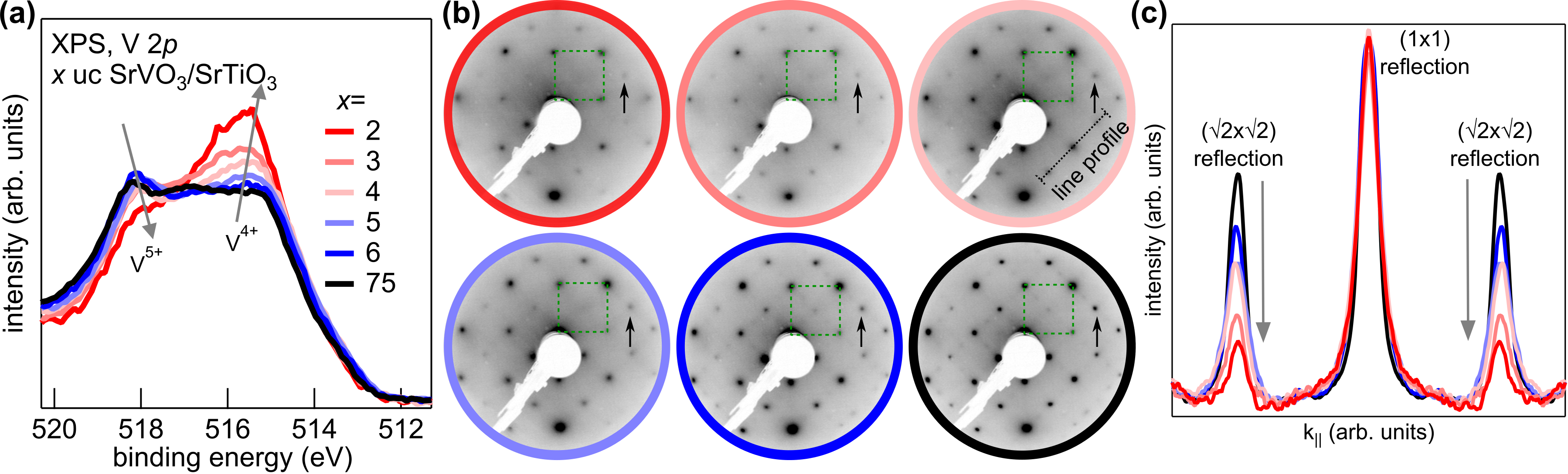
Figure 2a depicts the corresponding XPS V 2 spectra together with that of the 75 uc thick film, normalized to the integral V 2 spectral weight. The spectra exhibit a systematic trend:
The intensity of the V5+ component increases with the film thickness and saturates above 6 uc SVO.
To back up the observation in the V 2 spectra, we present the corresponding LEED patterns in Figure 2b, where the R(45∘) reconstruction ascribed to apical oxygen adsorption is present on all samples.
However, compared to the spots, the fractional order reflections (marked by the arrows) lose their intensity with decreasing film thickness.
This becomes apparent in Figure 2c in which the intensity of the LEED pattern is analyzed along the dotted line in 2b.
With the line profile normalized to the peak intensity of the reflection, the R(45∘) spots clearly weaken with decreasing SVO thickness, indicating a declining surface coverage with adsorbed oxygen, consistent with the trend revealed by XPS for the V5+ component in Figure 1a.
Note that the intensity changes in the diffraction pattern do not permit
a quantitative estimate of the total amount of adsorbed oxygen, as LEED detects only the ordered apical atoms incorporated in the superstructure and is not sensitive to oxygen adatoms randomly occupying the remaining apical sites.
Nonetheless, since the apparent trend detected in the LEED patterns mirrors that observed in the V 2 spectra, we arrive at the conclusion that the coverage of adsorbed apical oxygen and hence the fraction of V5+ ions gradually reduce with decreasing SVO film thickness.
3 Effect of the surface overoxidation – theory
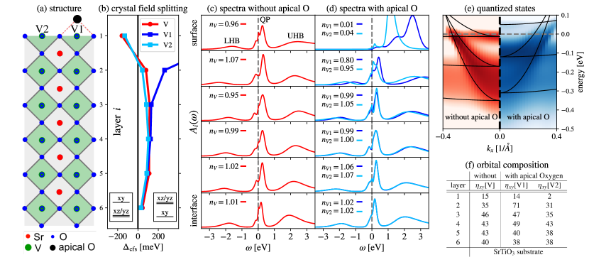
With the adsorbed oxygen draining electrons from the SVO films, we can expect their intrinsic low-energy electronic properties to be strongly modified with respect to fictitious bulk-like films with an ideal abrupt surface. To address this question, we perform realistic electronic structure calculations for 6 uc SVO on a STO substrate, using density functional theory (DFT) plus dynamical mean field theory (DMFT) with DFT structural relaxation. For computational details see the Methods section, and Section 5 in the Supporting Information for films of different thicknesses. Without apical oxygen, the surface layer shows a DFT crystal-field splitting of the V 3 shell between the (in-plane) -orbital and the (degenerate) orbitals of meV, see curve ”V” in Figure 3b. This splitting results from two competing effects: (i) the topmost vanadium atoms lack an apical oxygen to form a complete octahedron, which for an ideal cut-off octahedron would yield a value of meV;
(ii) the latter is slightly compensated by the structural relaxation as well as by the tensile strain imposed by the STO substrate which enhances the distance of the orbital lobes to the in-plane oxygens. [37] Accordingly, for the subsurface layers, where all oxygen octahedra are complete, is positive as seen in Figure 3b. Towards the STO substrate this effect is largely compensated by the (out-of-plane) lattice mismatch between SVO and STO.
Next, many-body effects are included using DMFT. Without apical oxygen, the spectral functions in Figure 3c are metallic for all layers, with the three-peak structure, consisting of lower Hubbard band, quasiparticle peak (with some fine structure) and upper Hubbard band, being prototypical for a correlated metal such as (bulk) SVO. All vanadium sites can be described with a nominal configuration (i.e., V4+). However, because of the layer-dependent crystal field splitting the orbital compositions differ vastly, see Figure 3f.
We now turn to the system with apical oxygen, where we consider the idealized experimental cell with 50% apical oxygen coverage. There are two inequivalent vanadium sites per layer, with and without apical oxygen, denoted “V1” and “V2”, respectively (see Figure 3a). The crystal field splitting for “V2” is similar to the case without oxygen in Figure 3b. The splitting for vanadium ions “V1”, however, is dramatically changed, even inverted, near the surface.
In all, apical oxygen-induced changes in the crystal and electronic structure are confined to the uppermost two layers, see the DMFT spectral functions in Figure 3d. Whereas the third to sixth layer are practically identical to the case without apical oxygen in Figure 3c, the top layer shows dramatic qualitative changes: it is insulating and contains only pentavalent vanadium with a occupation , i.e., no occupied states below the Fermi level at 0 eV (see Figure 3d, top row). The apical oxygen drains one electron from each of the two vanadium sites in the top layer, whereas the subsurface layers are again close to a V4+ configuration except for the V1 site of the second layer which has . With the apical oxygen draining all electrons from the surface layer, it becomes a dead (insulating) layer. The other layers then essentially behave as the film without apical oxygen but with one layer –the dead one– less. Because of the confinement to five layers (six without apical oxygen), quantum well states as shown in Figure 3e develop [13].
4 Effect of the surface overoxidation – experiment
To investigate experimentally the effect of the apical oxygen on the electronic structure, a 6 uc SVO/STO film was probed by soft x-ray photoelectron spectroscopy with the degree of surface overoxidation being varied in a controlled manner.
These measurements were performed with synchrotron radiation for two reasons. First, due to the tunability of the synchrotron light, core levels and valence band can be probed at the same photoelectron kinetic energy and thus the same probing depth.
We chose low photoelectron kinetic energies around 105 eV, at which the inelastic mean free path of the photoelectrons amounts to only 3.5Å , ensuring a high sensitivity to the topmost SVO layers (see Section 3 in the Supporting Information for the estimate of the inelastic mean free path).
Second, with the intense hard x-ray beam available at a third generation synchrotron the apical oxygen can be effectively removed through photon-induced desorption [38], thereby restoring a clean surface (see Methods).
Using these tactics, we have investigated the sample in two states:
(i) the state immediately after the PLD growth,
which is characterized by additional apical oxygen adsorbing on the VO2-terminated surface during the growth in an oxygen background pressure and which remains intact through an ultrahigh vacuum transfer to the synchrotron,
and (ii) the state after removal of the apical oxygen by irradiation of hard x-rays.
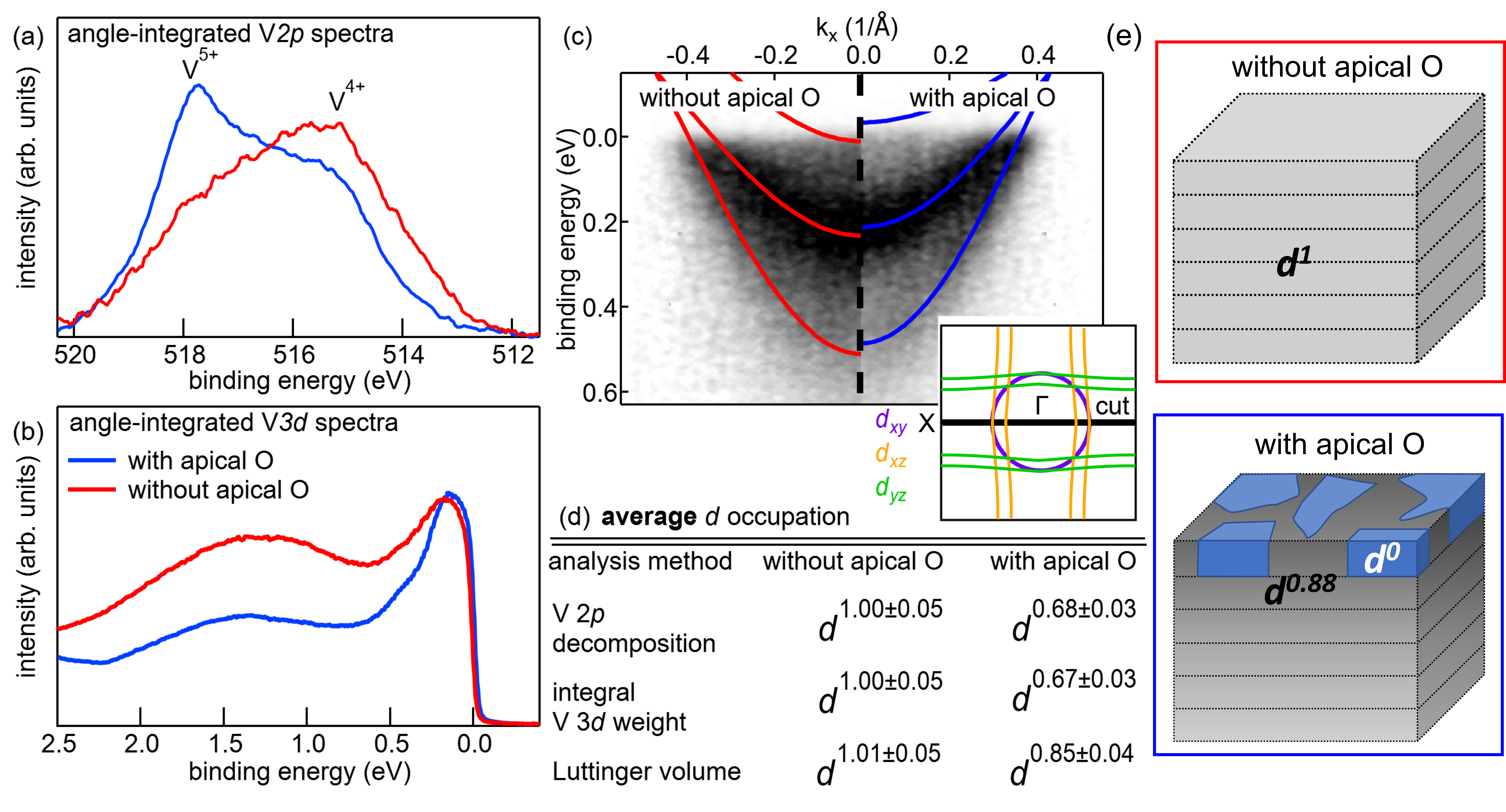
The corresponding V 2 spectra of the two states are presented in Figure 4a, where the presence and removal of apical oxygen for the states before (blue) and after (red) the hard x-ray exposure is confirmed by the pronounced and nearly quenched V5+ components, respectively, at 518 eV binding energy.
To quantify the effect of the apical oxygen on the electronic structure, we determine the V 3 occupations in both states using three different methods.
First, from a decomposition of the V 2 spectral weight into the V4+ and V5+ contributions we obtain and indicate in Figure 4d what we call the average occupation in the probed volume, i.e., the equivalent occupation of a homogeneous SVO film.
Based on the absence of a V5+ component in the V 2 spectra, the occupation of the film without apical oxygen is readily identified as .
When the surface is decorated with apical oxygen we find that the average occupation is lowered to (see Section 4 and Figure 5a in the Supporting Information for details).
An independent estimate of the average occupation can be obtained from the total (angle-integrated) V 3 weights for the two states, normalized to integration time.
The corresponding spectra are depicted in Figure 4b. The V 3 valence states span the first 2 eV below the Fermi level and display the characteristic line shape of a strongly correlated metal, featuring an incoherent lower Hubbard band (LHB) at about 1.5 eV and a metallic quasiparticle (QP) state at the Fermi level [22].
We find that the overall V 3 weight drops by 33% when the clean surface is compared to that with apical oxygen, in line with the 32% decrease in the average occupation inferred from the V 2 spectra (see Section 4 and Figure 5b in the Supporting Information for details).
Note that the presence or absence of apical oxygen not only affects the total intensity but also the line shape of the angle-integrated V 3 spectrum.
Yet another way of probing the V 3 band filling utilizes the determination of the Luttinger -space volume enclosed by the Fermi surface.
For this purpose, we evaluate the momentum-dependent band structure recorded by angle-resolved photoemission spectroscopy (ARPES).
Figure 4c shows band maps measured along the Brillouin zone cut sketched in the inset for the states with and without apical oxygen.
Assuming a 6 uc homogeneous SVO film, we derive the average band fillings from the observed Fermi wavevectors and the known symmetry and shape of the Fermi surface to be and for the states without and with apical oxygen, respectively, the values of which are also included in the table in Figure 4d for comparison (see Section 4 and Figure 5c-5e in the Supporting Information for details).
For the sample state of a clean surface, the table in Figure 4d shows that all three methods yield the same result, namely, essentially a occupation as expected from the nominal electron configuration of vanadium in stoichiometric SrVO3 (see top sketch in Figure 4e). In contrast, the resulting occupations differ noticeably for the state with apical oxygen:
while we observe larger than 30% reductions in the occupations inferred from the angle-integrated V 3 and V 2 spectra, the Luttinger volume derived from the angle-resolved V 3 measurements decreases by a much smaller amount of only 16% upon the addition of surface apical oxygen.
In general, such a discrepancy is indicative of an electronic phase separation into metallic and insulating regions on mesoscopic or microscopic length scales, as also observed for SrTiO3 [39].
This is because the band filling extracted from ARPES mapping is only susceptible to the metallic domains (as insulating regions do not contribute to the Fermi surface), whereas the angle-integrated V 3 and V 2 spectra average the band filling over both insulating and metallic domains and are insensitive to the spatial distribution of the electrons.
In light of this phase separation scenario, we consider the coexistence of insulating and metallic domains for the sample state with apical oxygen in line with the experimental results summarized in Figure 1 and the theoretical findings for the layer-resolved orbital occupations (see Figure 3d).
We model the SVO film by an inhomogeneous phase separation where laterally scattered domains are confined to the topmost layer and embedded in a homogeneous metallic matrix of band filling that extends 6 uc in depth, as shown in the bottom sketch of Figure 4e.
We vary and the surface coverage of the domains to yield the V5+/V4+ ratio and Luttinger volume that are consistent with the corresponding measured V 2 spectrum and ARPES band map.
Note that, while modelling the V 2 core level intensity, we take into account the exponential damping of the photoelectrons from sub-surface layers. We reproduce the experimental results for the 6 uc SVO film in the state with apical oxygen with a band filling for its metallic regions and (35)% of its surface turned into a dead layer.
It should be noted that the probing depth of our photoemission experiments amounts to about 10.5 Å (3-times the photoelectron inelastic mean free path given above), and sets a limit on the depth sensitivity of the angle-integrated measurements, and hence the above estimates are most relevant to the three topmost SVO layers.
Our findings of apical oxygen altering the electronic structure are at variance with the interpretation put forward by Backes et al.[40] of their synchrotron-based ARPES results on SVO films.
They observe strong changes in the spectral line shape as a function of UV irradiation and attribute them to beam-induced oxygen vacancies forming in the SVO lattice.
This interpretation is incompatible with our data, where the x-ray induced nearly 50% increase of V 3 spectral weight (Figure 4b) is accompanied by a massive V 2 spectral weight transfer from the V5+ to the V4+ component (Figure 4a), rather than any noticeable further reduction of V (from V4+ to V3+) expected for oxygen vacancy formation.
Note that their samples showing the large changes in spectral weight were transferred in air and then annealed in vacuum to recover a clean surface.
We suspect that the annealing process did not remove all the excess surface oxygen, which then desorbed under the intense UV light, as reported in this work.
Despite the different interpretations we observe essentially the same dependence of the V 3 spectral function on radiation dose.
5 Discussion
Viewed together, our theoretical and experimental results provide a detailed picture of the adsorption of oxygen at the apical sites of SVO films and its impact on their electronic properties.
The DMFT calculations consider the limiting case where every second vanadium in the film surface is decorated with an apical oxygen. They show that at this coverage the 3 shell of the V atoms in the topmost layer is completely depleted while the occupation of all layers beneath remains virtually unaffected.
For the 75 uc thick SVO film, whose apical oxygen coverage matches the supposition of the DMFT calculations, the formation of a complete layer at the surface is indeed observed experimentally in our depth-dependent XPS measurements.
We also find a phase forming in the surface layer of the 6 uc SVO film when decorated with apical oxygen. However, it does not cover the entire surface.
We observe additionally a slight electron depopulation of the metallic regions driven by the presence of apical oxygen.
The latter observation is elusive to our calculations which assume a full coverage of apical oxygen in an ordered R(45∘) arrangement.
Here it is interesting to note that the fractional order LEED reflections in Figure 2c are weaker for the 6 uc SVO film than for the 75 uc one, suggesting that, unlike the much thicker film where the coverage of the R(45∘) reconstruction is more complete, the surface of the 6 uc SVO film should have regions covered by apical oxygen ions that do not follow the same long range order as well as regions covered by less apical oxygen.
There, the local lattice distortion and thus the crystal field splitting may be reduced and favor light doping of the film instead of complete depletion of the band of the surface layer.
Beside the change in the occupation, we also observe that the V 3 spectral shape begins to evolve upon the desorption of apical oxygen.
With the V 3 weight exclusively originating from the metallic domains, this indicates a variation in their electronic properties.
In particular, the apparent increase in the ratio of the LHB and QP weights may signal increased correlations in the absence of apical oxygen, which might be partly explained by the occupation being driven closer to an integer filling.
Furthermore, the topmost layer of the SVO film can exhibit enhanced correlations due to reduced coordination numbers
[41, 24] and thus a different QP to LHB ratio from the bulk.
The presence of domains in the topmost layers of the film with adsorbed oxygen will suppress this surface contribution and alter the V 3 spectral function.
Alternatively, defects in the topmost layer may lead to enhanced scattering and hence broadening of the QP feature.
When domains develop with the adsorption of apical oxygen, surface defects are shielded by the dead layer,
scattering becomes less important, and the V lineshape will feature a sharper QP peak.
We have demonstrated that the presence of apical oxygen can have a strong bearing on the electronic properties of ultrathin SVO films in terms of the layer-dependent crystal-field splitting, occupation, number of quantum well states, and orbital composition. In addition, we observe electronic phase separation, in both lateral and vertical directions, into metallic and insulating domains.
Since the apical oxygen changes the electronic structure in the same thickness range in which also the transition from a correlated metal into a Mott insulating phase [12] occurs,
it is a natural step to link these two phenomena.
While we can safely assert that the metal-insulator transition is influenced in many ways by surface chemical effects and that a description
within a simple Mott-Hubbard type scenario falls short, a full understanding of the complex interplay between the thickness-dependent electronic transition and
the adsorption of apical oxygen requires further studies and is beyond the scope of the present work.
In view of the fact that TMO thin films are often grown on the TiO2 terminated SrTiO3 surface which results in a BO2 terminated thin film, apical oxygen is a widespread phenomenon for ultrathin TMO films. [16, 17, 4].
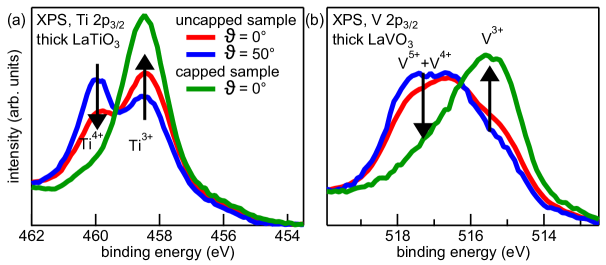
Figure 5a exemplarily illustrates that the presented scenario is also observed in LaTiO3 [4] and LaVO3 [42] thin films.
While stoichiometric LaTiO3 and LaVO3 films would be identified by Ti3+ and V3+ valence states, signals characteristic of Ti4+ and V4+ and V5+ valence states are seen in bare LaTiO3 and LaVO3 films.
As for the SVO, these signals decrease with the electron emission angle, which confirms that they are induced by surface overoxidation.
Oxygen adatoms are likely to also show up at the surface of other non-perovskite crystal structures at which the metal-oxygen ligand octahedron is broken.[19, 20, 21, 18]
Figure 5 also demonstrates
an effective way of preventing the surface overoxidation:
capping the films with an isostructural and inert epitaxial oxide layer which restores the correct stoichiometry and stabilizes the pristine bulk valence states.
6 Conclusion
Using the example of SVO we demonstrated that apical oxygen, which decorates the surface of a TMO film may severely alter the intrinsic electronic structure in a multitude of ways. The apical oxygen can lead to the formation of an electronically and magnetically dead layer with a occupation at the surface and can furthermore change the strength of electronic correlations, the scattering and the band filling in the metallic layers. These findings illustrate that the detailed oxygen configuration at the surface, including surface apical oxygen but also potential capping layers, has to be considered for a microscopic understanding of transition metal oxide thin films in experiment and theory. It is, in particular, essential for the design and operation of nanoscale devices.
7 Methods
The SVO thin films were deposited by pulsed laser deposition (PLD) on the TiO2-terminated (001) surfaces of STO substrates, which were prepared following reference [43]. Every substrate was checked by atomic force microscopy before growth and exhibited an atomically flat surface with terrace steps of single unit cell height.
The SVO films were fabricated in a high vacuum (oxygen background pressure mbar) at a substrate temperature of 650 ∘C by ablation from a polycrystalline SrVO3+x pellet employing a KrF excimer laser at a laser fluence of 0.50 J/cm2 and a pulse repetition rate of 10 Hz. The target-substrate distance amounted to 54 mm.
The growth of the SVO films was monitored by reflection high-energy electron diffraction. The high sample quality was confirmed by x-ray diffraction and electric transport measurements (see Section 1 in the Supporting Information).
The XPS data shown in Figure 1 and 2 was recorded with a monochromatized Al laboratory source and an Omicron EA-125 analyzer.
The photoemission experiments presented in Figure 4 were conducted at the
two-color beamline I09 at Diamond Light Source.
The samples were oriented with LEED before the photoemission measurements at the synchrotron.
The V 3 and V 2 spectra were probed with linearly polarized soft x-rays at a photon energy of 105 and 610 eV, respectively.
An intense hard x-ray beam at 3 keV photon energy focused onto the same spot as the soft x-ray beam[44] was used to desorb the apical oxygen. The spot size of both x-ray beams is 30m 50m.
The spectra were acquired with a EW4000 photoelectron analyzer (VG Scienta, Uppsala, Sweden) equipped with a wide angle acceptance lens (acceptance angle parallel to analyzer slit 60∘, perpendicular to analyzer slit 0.3∘).
An inelastic mean free path of 3.5Å and 18Å was used to model the V 2 spectra measured at a photoelectron kinetic energy of 105 eV and 970 eV, respectively.
In DFT the heterostructures were prepared with layers SrVO3 on top of 5 layers SrTiO3 oriented in the (001)-direction where the final termination of the surface SrVO3 layer is VO2.
The structure without apical oxygen was set up with the constrained in-plane lattice constant of bulk SrTiO3 () while the structure
with apical oxygen was implemented as a supercell () with every other surface vanadium being connected to an additional apical oxygen atom.
Above the film, a sufficiently large vacuum layer of roughly Å was added in (001)-direction.
The atomic positions of the SrTiO3 layer furthest away from the surface SrVO3 were kept fixed, all other atomic positions were completely relaxed using VASP[45, 46, 47, 48].
The full-electron DFT calculation of these structures were then performed with WIEN2k[49], where we verified the consistency of the internal forces between the two codes.
All DFT calculations employed the PBE exchange-correlation potential[45].
The down-folding to a localized Hamiltonian was done with the Wien2Wannier[50] interface to Wannier90 [51]. Here we projected purely
onto the orbitals of the () inequivalent vanadium sites of the structures without (with) apical oxygen.
The resulting Hamiltonian was then supplemented with a layer-independent SU-symmetric Kanamori interaction eV, eV, eV.
These values were chosen to deviate slightly from the more typical bulk SrVO3 values in literature[52] (eV, eV, eV) to mimic slightly smaller screening effects in the quasi-two-dimensional structure[35].
We performed the DMFT calculations at room temperature (eV-1; K) with a continuous-time quantum Monte Carlo solver, employing a orbital-diagonal hybridization function, using w2dynamics[53].
To obtain the spectral functions on the real frequency axis, the resulting Green’s functions on the Matsubara axis were analytically continued using the maximum entropy method[54, 55] implemented in ana_cont[56].
Acknowledgements
The authors gratefully acknowledge funding support from the Deutsche Forschungsgemeinschaft (DFG) through the Würzburg-Dresden Cluster of Excellence on Complexity and Topology in Quantum Matter “ct.qmat” (EXC 2147, Project ID 390858490) as well as through the Collaborative Research Center SFB 1170 “ToCoTronics” (Project ID 258499086) and from the Austrian Science Fund (FWF) through grants P 30819, P 30997, P 32044, and P 30213.
We also wish to thank Diamond Light Source for time on beamline I09 under proposals SI23737 and SI25151 and D. McCue for his superb technical support at the I09 beamline.
The authors gratefully acknowledge access to the Vienna Scientific Cluster (VSC) and thank the Gauss Centre for Supercomputing e.V. (www.gauss-centre.eu) for providing computing time on SuperMUC-NG at the Leibniz Supercomputing Centre (www.lrz.de).
J.G. and M.P. contributed equally to this work.
Supporting Information
Supporting Information is available from the Wiley Online Library or from the author.
References
- [1] C. H. Ahn, J.-M. Triscone, J. Mannhart, Nature 2003, 424, 6952 1015.
- [2] J. Heber, Nature 2009, 459, 7243 28.
- [3] J. Son, S. Rajan, S. Stemmer, S. James Allen, J. Appl. Phys. (Melville, NY, U. S.) 2011, 110, 8 084503.
- [4] P. Scheiderer, M. Schmitt, J. Gabel, M. Zapf, M. Stübinger, P. Schütz, L. Dudy, C. Schlueter, T.-L. Lee, M. Sing, R. Claessen, Adv. Mater. 2018, 30, 25 1706708.
- [5] D. M. Newns, J. A. Misewich, C. C. Tsuei, A. Gupta, B. A. Scott, A. Schrott, Appl. Phys. Lett. 1998, 73, 6 780.
- [6] M. Gu, J. Laverock, B. Chen, K. E. Smith, S. A. Wolf, J. Lu, J. Appl. Phys. (Melville, NY, U. S.) 2013, 113, 13 133704.
- [7] R. Scherwitzl, S. Gariglio, M. Gabay, P. Zubko, M. Gibert, J.-M. Triscone, Phys. Rev. Lett. 2011, 106, 24 246403.
- [8] D. Toyota, I. Ohkubo, H. Kumigashira, M. Oshima, T. Ohnishi, M. Lippmaa, M. Takizawa, A. Fujimori, K. Ono, M. Kawasaki, H. Koinuma, Appl. Phys. Lett. 2005, 87, 16 162508.
- [9] J. Xia, W. Siemons, G. Koster, M. R. Beasley, A. Kapitulnik, Phys. Rev. B 2009, 79, 14 140407.
- [10] J. M. Rondinelli, N. M. Caffrey, S. Sanvito, N. A. Spaldin, Phys. Rev. B 2008, 78, 15 155107.
- [11] P. Schütz, D. Di Sante, L. Dudy, J. Gabel, M. Stübinger, M. Kamp, Y. Huang, M. Capone, M.-A. Husanu, V. N. Strocov, G. Sangiovanni, M. Sing, R. Claessen, Phys. Rev. Lett. 2017, 119, 25 256404.
- [12] K. Yoshimatsu, T. Okabe, H. Kumigashira, S. Okamoto, S. Aizaki, A. Fujimori, M. Oshima, Phys. Rev. Lett. 2010, 104, 14 147601.
- [13] K. Yoshimatsu, K. Horiba, H. Kumigashira, T. Yoshida, A. Fujimori, M. Oshima, Science 2011, 333, 6040 319.
- [14] M. Takizawa, M. Minohara, H. Kumigashira, D. Toyota, M. Oshima, H. Wadati, T. Yoshida, A. Fujimori, M. Lippmaa, M. Kawasaki, H. Koinuma, G. Sordi, M. Rozenberg, Phys. Rev. B 2009, 80, 23 235104.
- [15] Y. Okada, S.-Y. Shiau, T.-R. Chang, G. Chang, M. Kobayashi, R. Shimizu, H.-T. Jeng, S. Shiraki, H. Kumigashira, A. Bansil, H. Lin, T. Hitosugi, Phys. Rev. Lett. 2017, 119, 8 086801.
- [16] K. Fuchigami, Z. Gai, T. Z. Ward, L. F. Yin, P. C. Snijders, E. W. Plummer, J. Shen, Phys. Rev. Lett. 2009, 102, 6 066104.
- [17] P. Schütz, M. Kamp, D. Di Sante, A. Lubk, B. Büchner, G. Sangiovanni, M. Sing, R. Claessen, Appl. Phys. Lett. 2020, 116, 20 201601.
- [18] M. J. Wahila, N. F. Quackenbush, J. T. Sadowski, J.-O. Krisponeit, J. I. Flege, R. Tran, S. P. Ong, C. Schlueter, T.-L. Lee, M. E. Holtz, D. A. Muller, H. Paik, D. G. Schlom, W.-C. Lee, L. F. J. Piper, (Preprint) arXiv:2012.05306, v1, submitted: December 2020 .
- [19] A. J. Window, A. Hentz, D. C. Sheppard, G. S. Parkinson, H. Niehus, D. Ahlbehrendt, T. C. Q. Noakes, P. Bailey, D. P. Woodruff, Phys. Rev. Lett. 2011, 107 016105.
- [20] F. E. Feiten, J. Seifert, J. Paier, H. Kuhlenbeck, H. Winter, J. Sauer, H.-J. Freund, Phys. Rev. Lett. 2015, 114 216101.
- [21] G. Lantz, M. Hajlaoui, E. Papalazarou, V. L. R. Jacques, A. Mazzotti, M. Marsi, S. Lupi, M. Amati, L. Gregoratti, L. Si, Z. Zhong, K. Held, Phys. Rev. Lett. 2015, 115 236802.
- [22] A. Fujimori, I. Hase, H. Namatame, Y. Fujishima, Y. Tokura, H. Eisaki, S. Uchida, K. Takegahara, F. M. F. de Groot, Phys. Rev. Lett. 1992, 69, 12 1796.
- [23] I. H. Inoue, I. Hase, Y. Aiura, A. Fujimori, Y. Haruyama, T. Maruyama, Y. Nishihara, Phys. Rev. Lett. 1995, 74, 13 2539.
- [24] A. Sekiyama, H. Fujiwara, S. Imada, S. Suga, H. Eisaki, S. I. Uchida, K. Takegahara, H. Harima, Y. Saitoh, I. A. Nekrasov, G. Keller, D. E. Kondakov, A. V. Kozhevnikov, T. Pruschke, K. Held, D. Vollhardt, V. I. Anisimov, Phys. Rev. Lett. 2004, 93, 15 156402.
- [25] M. J. Rozenberg, I. H. Inoue, H. Makino, F. Iga, Y. Nishihara, Phys. Rev. Lett. 1996, 76, 25 4781.
- [26] E. Pavarini, A. Yamasaki, J. Nuss, O. K. Andersen, New J. Phys. 2005, 7, 1 188.
- [27] H. Lee, K. Foyevtsova, J. Ferber, M. Aichhorn, H. O. Jeschke, R. Valentí, Phys. Rev. B 2012, 85, 16 165103.
- [28] J. M. Tomczak, M. Casula, T. Miyake, F. Aryasetiawan, S. Biermann, Europhys. Lett. 2012, 100, 6 67001.
- [29] C. Taranto, M. Kaltak, N. Parragh, G. Sangiovanni, G. Kresse, A. Toschi, K. Held, Phys. Rev. B 2013, 88, 16 165119.
- [30] J. M. Tomczak, M. Casula, T. Miyake, S. Biermann, Phys. Rev. B 2014, 90, 16 165138.
- [31] A. v. Roekeghem, S. Biermann, Europhys. Lett. 2014, 108, 5 57003.
- [32] J. A. Moyer, C. Eaton, R. Engel-Herbert, Adv. Mater. 2013, 25, 26 3578.
- [33] L. Zhang, Y. Zhou, L. Guo, W. Zhao, A. Barnes, H.-T. Zhang, C. Eaton, Y. Zheng, M. Brahlek, H. F. Haneef, N. J. Podraza, M. H. W. Chan, V. Gopalan, K. M. Rabe, R. Engel-Herbert, Nat. Mater. 2016, 15, 2 204.
- [34] L. Si, J. Kaufmann, Z. Zhong, J. M. Tomczak, K. Held, Phys. Rev. B 2021, 104 L041112.
- [35] Z. Zhong, M. Wallerberger, J. M. Tomczak, C. Taranto, N. Parragh, A. Toschi, G. Sangiovanni, K. Held, Phys. Rev. Lett. 2015, 114, 24 246401.
- [36] G. Silversmit, D. Depla, H. Poelman, G. B. Marin, R. De Gryse, J. Electron Spectrosc. Relat. Phenom. 2004, 135, 2-3 167.
- [37] M. Pickem, J. Kaufmann, K. Held, J. M. Tomczak, Phys. Rev. B 2021, 104 024307.
- [38] M. L. Knotek, P. J. Feibelman, Phys. Rev. Lett. 1978, 40, 14 964.
- [39] L. Dudy, M. Sing, P. Scheiderer, J. D. Denlinger, P. Schütz, J. Gabel, M. Buchwald, C. Schlueter, T.-L. Lee, R. Claessen, Adv. Mater. 2016, 28, 34 7443.
- [40] S. Backes, T. C. Rödel, F. Fortuna, E. Frantzeskakis, P. Le Fère, F. Bertran, M. Kobayashi, R. Yukawa, T. Mitsuhashi, M. Kitamura, K. Horiba, H. Kumigashira, R. Saint-Martin, A. Fouchet, B. Berini, Y. Dumont, A. J. Kim, F. Lechermann, H. O. Jeschke, M. J. Rozenberg, R. Valentí, A. F. Santander-Syro, Phys. Rev. B 2016, 94, 24 241110.
- [41] A. Liebsch, Phys. Rev. Lett. 2003, 90, 9 096401.
- [42] M. Stübinger, J. Gabel, P. Scheiderer, M. Zapf, M. Schmitt, P. Schütz, B. Leikert, J. Küspert, M. Kamp, P. K. Thakur, T.-L. Lee, P. Potapov, A. Lubk, B. Büchner, M. Sing, R. Claessen, Phys. Rev. B 2021, 103 235128.
- [43] G. Koster, B. L. Kropman, G. J. H. M. Rijnders, D. H. A. Blank, H. Rogalla, Appl. Phys. Lett. 1998, 73, 20 2920.
- [44] J. Gabel, M. Zapf, P. Scheiderer, P. Schütz, L. Dudy, M. Stübinger, C. Schlueter, T.-L. Lee, M. Sing, R. Claessen, Phys. Rev. B 2017, 95, 19 195109.
- [45] J. P. Perdew, K. Burke, M. Ernzerhof, Phys. Rev. Lett. 1996, 77, 18 3865.
- [46] G. Kresse, J. Hafner, Phys. Rev. B 1993, 47 558.
- [47] G. Kresse, J. Hafner, Phys. Rev. B 1994, 49 14251.
- [48] G. Kresse, J. Furthmüller, Comput. Mater. Sci. 1996, 6, 1 15 .
- [49] P. Blaha, K. Schwarz, G.-K.-H. Madsen, D. Kvasnicka, J. Luitz, Vienna University of Technology, Austria 2001, ISBN 3-9501031-1-2.
- [50] J. Kunes, R. Arita, P. Wissgott, A. Toschi, H. Ikeda, K. Held, Comput. Phys. Commun. 2010, 181, 11 1888 .
- [51] A. Mostofi, J. Yates, G. G Pizzi, Y. Lee, I. Souza, D. Vanderbilt, N. Marzari, Comput. Phys. Commun. 2014, 185 2309.
- [52] E. Pavarini, S. Biermann, A. Poteryaev, A. I. Lichtenstein, A. Georges, O. K. Andersen, Phys. Rev. Lett. 2004, 92 176403.
- [53] M. Wallerberger, A. Hausoel, P. Gunacker, A. Kowalski, N. Parragh, F. Goth, K. Held, G. Sangiovanni, Comput. Phys. Commun. 2019, 235 388 .
- [54] M. Jarrell, J. Gubernatis, Phys. Rep. 1996, 269, 3 133.
- [55] D. Geffroy, J. Kaufmann, A. Hariki, P. Gunacker, A. Hausoel, J. Kuneš, Phys. Rev. Lett. 2019, 122 127601.
- [56] J. Kaufmann, K. Held, (Preprint) arXiV:2105.11211, v1, submitted: May 2021 .