suppmat_REV2_1502
Spintronic THz emitters based on transition metals and semi-metals/Pt multilayers.
Abstract
Spintronic terahertz (THz) emitters (STE) based on the inverse spin Hall effect in ferromagnetic/heavy metal (FM/HM) heterostructures have become important sources for THz pulse generation. The design, materials and control of these interfaces at the nanometer level has become vital to engineer their THz emission properties. In this work, we present studies of the optimization of such structures through a multi-pronged approach, taking advantage of material and interface engineering to enhance the THz spintronic emission. This includes: the application of multi-stacks of HM/FM junctions and their application to trilayer structures; the use of spin-sinks to simultaneously enhance the THz emitted fields and reduce the use of thick Pt layers to reduce optical absorption; and the use of semi-metals to increase the spin polarization and thus the THz emission. Through these approaches, significant enhancements of the THz field can be achieved. Importantly, taking into account the optical absorption permits to elucidate novel phenomena such as the relation between the spin diffusion length and the spin-sink using THz spectroscopy, as well as possibly distinguishing between self– and interface- spin-to-charge conversion in semi-metals.
Spintronic terahertz (THz) emitters (STE) have considerably impacted THz technology in a remarkably short time frame [1, 2, 3, 4], becoming a viable and alternative source to nonlinear crystals and photoconductive antennas for THz time-domain spectroscopy (TDS). These structures typically consist of nanometer thick ferromagnetic (FM) - heavy metal (HM) junctions. When optically excited with a femtosecond near-infrared (NIR) laser, an out-of-equilibrium spin current is generated in the former, the so-called superdiffusive flux [5, 6], that is converted to a transient charge-current in the latter - spin-to-charge conversion (SCC) - via the inverse spin Hall effect (ISHE). This current then gives rise to a linearly polarized THz pulse where the polarization can be easily controlled by a small applied magnetic field. Compared to other established technologies, THz spintronic sources have the advantages of generating phonon-less THz spectra, being extremely thin, with performances surpassing those of thick (hundreds of microns) nonlinear crystals. As well as an important THz technology, THz emission TDS has now proven to be an essential tool to probe ultrafast spintronic phenomena at FM/HM interfaces as well as in a range of novel materials, from topological insulators to transition metal dichalcogenides [7, 8].
While FM/HM based interfaces such as W/Co40Fe40B20/Pt [1] represent the materials of reference, this letter presents routes towards THz emitters using engineered spintronic interfaces to reach higher THz fields, as well as enhancing our understanding of THz SCC. More specifically, beyond tuning the excitation wavelength [9, 10, 11, 12], improvements in the THz emission efficiency via the ISHE in HM based junctions are anticipated by considering three major strategies: i) metallic multi-stacks of spintronic junctions of high electronic transparency [13, 14, 15, 16] allowing a large number of emitting dipole planes, but sufficiently thin to minimise NIR and THz optical absorption; ii) by optimized stacks coupled with specific spin-sinks such as Au:W alloys [17, 18, 19, 20] to avoid detrimental hot spin reflection, where we show theoretically and experimentally in the limit of thin films ( 2 nm) a large gain in the THz E-field; iii) by means of optically excited spin-polarization enhancement with the use of semi-metals such as those based on Heusler compounds (presently Co2MnGa) possessing an intrinsic high spin-polarization.
In this paper, by exploiting the properties of transition metal interfaces, we explore these three different aspects and show that the STE electronic efficiency may be enhanced by at least a factor 2 for the emitted THz field and thus power enhancements by a factor 4. Importantly, to explain these enhancements, we analyse our results when stripped from the effect of optical (NIR and THz) absorption to highlight the intrinsic physics of SCC at play. In particular, the THz absorption plays a detrimental role in the signal reduction by a typical factor lying between 2 and 4 (output power reduced by one order of magnitude). In all experiments, the STEs are excited by a Ti:Sa oscillator delivering 100 fs pulses centered at 810 nm and the emitted THz pulses are detected using electro-optic sampling in a THz-TDS system (see Suppl. Mat. S1).
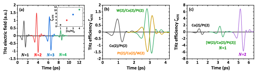
As a proof of concept, our first approach to investigate THz emission of STE FM/HM structures is to grow periodic stacks of thin Co/Pt layers to increase the total emitting dipoles and hence the ultrafast spin-current generation [21, 22, 23]. [Co(2)/Pt(2)]N multi-stack samples were grown on glass substrates with the number in parenthesis indicating the thickness of the layer in nanometers and the number of periods (1, 2, 3 and 4) with a 1 nm thick AlOx separating each period in order to avoid opposite charge dipoles within the structures (details in Suppl. Mat S1). The emitted THz fields are shown in Fig. 1a showing that provides the strongest by a factor 1.5 in respect to the reference. The THz signal decreases for by a factor 1.25, 5 respectively which can be understood by a larger NIR and THz absorption on increasing the periods. This indicates that corresponds to the best compromise between the added dipoles planes contributing to and the wave absorption. The withdrawal of NIR and THz absorption contributions to the THz emission for each repetition period (Suppl. Mat. S3 and associated references [24, 25, 26]) as shown in the inset of Fig. 1a allows the introduction of the STE electronic efficiency . The latter quantity refers, also for the forward discussions, to the effective spin relaxation length in Pt (HM) for the hot electron spin-current. Interestingly, this shows a linear behaviour of the THz field for increasing number of Co/Pt period and indicates that the limiting factor is the optical absorption for the THz generation.
As shown by Seifert et. al. [1], another approach towards signal enhancement is to design trilayers involving a FM layer embedded between two HMs of opposite spin Hall angle signs (resp. Pt and W), thus harvesting opposite spin currents. Here the different contributions of SCC from each HM interface interfere constructively, resulting in an enhanced . Fig. 1b compares the THz pulses compensated from NIR and THz absorption from W(2)/Co(2)/Pt(2) and Pt(2)/Co(2)/W(2) samples grown by the same method to a Co(2)/Pt(2) reference. The THz signal reaches factors of 1.7 and 1.4 for W(2)/Co(2)/Pt(2) and Pt(2)/Co(2)/W(2) multilayers respectively. As expected by the spin Hall angle of the first metal excited by the fs oscillator (Pt in W(2)/Co(2)/Pt(2) and W in Pt(2)/Co(2)/W(2)), the phase of the THz pulse reverts accordingly. Merging now the periodic stacks and trilayers concepts, samples of [W(2)/Co(2)/Pt(2)]2 with 1 nm AlOx separators between the periods were realized. The results shown in Fig. 1c clearly show a STE electronic efficiency enhanced by a factor 7.5 with respect to the Co/Pt reference when the optical absorption is withdrawn. This layer repetition approach demonstrates the crucial limitation of both NIR and THz absorption in STE structures. The same overall qualitative and quantitative conclusions are raised by replacing Co by Co40Fe40B20 by comparing results from [W/Co40Fe40B20/Pt]1 and [W/Co40Fe40B20/Pt]2 trilayers as shown on Fig. 1c.
The modeling of the THz emission of periodic structures requires the expression of emitted from the multiple dipole planes according to Refs. [25, 24] and Suppl. Mat. S2 which includes multiple reflections consideration in the multilayered structures:
| (1) |
where is the free space impedance, is the optical index of the substrate, is the conductivity of a single period integrated over its thickness and the maximum numbers of the dipole planes excited by optical absorption (ratio of the NIR absorption depth nm [27] over the metallic multilayer period , presently 6 nm). The optimum is obtained by minimizing Eq. 1 over giving in fine 1 once considered the numerical parameters. The calculation gives an optimal value of in agreement with experiments ().
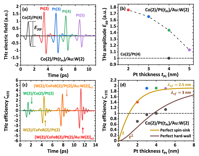
The second part of this work is the application of metallic spin-sinks [28] as a method to optimize STEs. Here, we propose the use of Au:W alloys possessing the advantage of a high spin interface transparency [15, 29] with Pt along with a large resistivity (.cm). This makes Au:W alloys perfect candidates to avoid spin backflow at the outward Pt interface. More details about the Au:W allow deposition can be found in Suppl. Mat. S1. The samples studied were a Co(2)/Pt()/Au:W(2) series deposited on MgO(). Fig. 2a displays the acquired THz pulses mapped by THz-TDS for different Pt thickness and 5 nm; Fig. 2b displays the THz peak-to-peak amplitude for each sample. THz pulses are compared to the reference Co(2)/Pt(4) grown within the same batch. The THz emission from Co(2)/Pt(4)/Au:W(2) is almost 50% larger than the emission from Co(2)/Pt(4) one, despite the latter being characterized by having a smaller optical absorption (both THz and NIR), illustrating the significant spin-sink effect (SSE) using Au:W in the sub-picosecond domain. A subsequent increase of the THz emission efficiency is also observed for the whole series nm (Fig. 2d). Moreover, by comparing the results obtained for different Pt thicknesses, one evidences an even larger emission efficiency for nm by almost 80% compared to Co(2)/Pt(4). These results are in favor of a strong SSE enhanced by the ability of reducing the THz absorption through the reduction of the Pt thickness of a large conductance (.cm). The drop of the THz pulse amplitude for nm from its maximal value follows from a smaller SSE as exceeds its spin-relaxation length as well as to a larger THz absorption (THz and NIR pump). Fig. 2c presents the renormalized THz emission after having taken into account the THz and NIR absorptions in the layered structures. This gives the STE electronic efficiency . We notice that below the electronic spin relaxation length (3 nm for Pt), the conversion builds-up until it saturates after the relaxation length: this expected behaviour is in line with ISHE. At comparable structure thickness (i.e. Pt(4)), the addition of Au:W(2) allows to increase the conversion efficiency by nearly a factor of 2 in field. A particular interesting point is the observation of a same increase of with the inclusion of Au:W spin-sink in [W(2)/CoFeB(2)/Pt(2)/Au:W(2)]2 compared to W(2)/CoFeB(2)/Pt(2)/Au:W(2) owing to avoiding backward majoritary spin-current reflection.
The effect of the spin-sink layer can be modelled with the assumption of the existence of effective momentum and spin relaxation lengths in the THz domain in the wave-diffusion approach [30, 31, 13]. More details on the ultrafast electron diffusion model are discussed in Suppl. Mat. S3. We are searching the STE efficiency and subsequent SCC integrated over the Pt thickness. The expression of can be generalized in terms of a three-layers model and may found for the two limiting cases of i) a perfect hard-wall or perfect (detrimental) spin reflections at the top Pt and ii) a perfect spin-sink as approached by Au:W yielding in fine to:
| (2) |
with the spin-relaxation length, the volume of the time-oscillating dipoles.
The perfect spin-sink (ss) corresponds to a zero spin-resistance i.e that is no spin-accumulation at its interface with Pt. The perfect hard-wall (hw) limit corresponds to an infinite spin-resistance giving zero spin-current and a maximum spin-accumulation. The two expressions of Eq. (2) match well the variation of the renormalized THz emission experimentally observed in Fig. 2c with nm, with and the respective Co and Pt spin-resistance (Ref. [32]) in unit of the inverse of the Sharvin resistance . The positive action of the spin-sink is obtained by considering the expression of (Eq. (2)) and its dependence vs. . The quantitative gain in can be also traced by considering the figure of merit :
| (3) |
which manifests a gain ratio in the spin-injection efficiency .
The gain in the STE electronic efficiency goes to zero in the limit of infinite Pt thickness, . On the other hand, goes to infinite in the limit of small . This is due to a linear increase of in for a perfect spin-sink whereas only a quadratic increase of in is expected for a hard-wall system. As an example, we have plotted on Fig. 2c the expected obtained from the two opposite situations of a perfect spin-sink and of a hard-wall for at the vicinity of . Fig. 2c and the corresponding guidelines express that Co(2)/Pt(1)/Au:W(2) gives an equivalent signal in size to Co(2)/Pt(4) from a pure electronic efficiency point-of-view with, however, the benefit of a reduced THz absorption. The results is also true for Co(2)/Pt(2)/Au:W(2). It leads to the extraction of a spin diffusion length nm on MgO in close agreement with values assigned in the literature for the present Pt conductivity [33, 34, 35]. The field amplitude is the product of , an increasing function of , times a product of two decreasing functions vs. related to the NIR and THz absorptions (see Eq. (ES1) in the Suppl. Mat. S2). The analysis yields an optimum of in both spin-sink and hard-wall systems. The values of which yields a maximum for different nm are given in Table I in the two cases. An optimal value of nm for the spin-sink limit on Fig. 2b well corresponds to nm as previously determined. Table I also presents the effective reduction of the optimal Pt thickness for the two models resulting in a coupled effect of spin-sink electronic enhancement and reduction of the optical absorptions thus allowing a significant emission increase.
| (nm) | 1 | 2 | 3 | 4 | 5 | 7 | 10 |
|---|---|---|---|---|---|---|---|
| (nm) | 1.1 | 1.7 | 2.1 | 2.4 | 2.6 | 3 | 3.4 |
| (nm) | 2.2 | 3.3 | 4.1 | 4.6 | 5.3 | 6.2 | 7 |
| (%) | -50 | -48 | -48 | -48 | -51 | -52 | -51 |
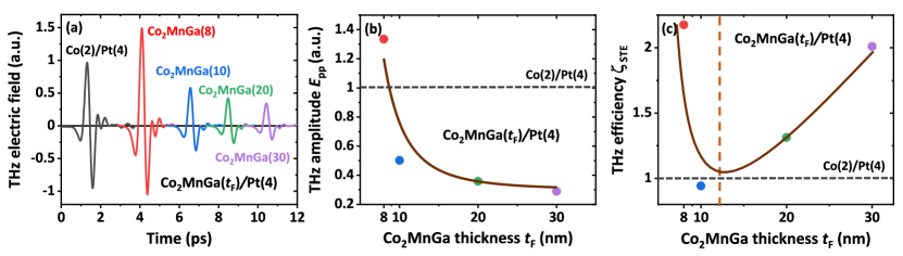
Finally, we now turn to the role of the spin injector in the THz emission efficiency and particularly on the one of STEs based on magnetic Weyl half-metal Heusler alloys exceeding the one of the best CoFeB 3d transition metal candidate. The integration of such members of the Heusler family, presently Co2MnGa, in active STEs [36, 37, 38] has several potential advantages and few drawbacks. First, such magnetic Weyl materials are known to i) behave as half-metals possessing a strong spin polarization connected to a majoritary spin-down reservoir [39, 40, 41] and ii) possess a high transparency with Pt comparable to Co/Pt in connection to a large experimental spin-mixing conductance with Pt from spin-pumping [42, 43]. Moreover, Co2MnGa has recently been demonstrated to carry a negative spin Hall angle % (the sign is compared to Pt) owing to their spin-orbit and subsequent Berry phase [44]. One may also expect strong THz emission of a single Co2MnGa film (self-emission) [45] with a reduced conductivity (130 .cm [46]) reducing the THz absorption based on the Drude model [47]. All these arguments account for an ideal THz emission recipe. The samples investigated here were MgO//Co2MnGa()/Pt(4) structures (see Suppl. Mat. S1).
We present in Figs. 3a and 3b the Co2MnGa()/Pt thickness dependence (resp. 8, 10, 20, 30 nm) of the THz emission. Notably, at =8 nm, the generated THz pulse is still 35% larger than the Co(2)/Pt(4) even if the spin-injector is four times thicker. This shows that Co2MnGa is a more efficient spin-injector compared to Co and emphases the strong spin polarization of this Heusler compound. Moreover, the THz pulse generated from a single Co2MnGa(43) layer (Suppl. Mat. S4) is negligible compared to Co2MnGa(43)/Pt bilayers. It may indicate the expected self-SCC contribution although its relative small amplitude. Figs. 3a and 3b show that an increase of the Co2MnGa thickness reduces the emitted THz amplitude in line with optical absorption. To take into account these effects, we proceeded as previously to the THz and NIR renormalization procedure (see Suppl. Mat. S2) in order to extract the STE electronic efficiency . The tabulated results are presented in Fig. 3c.
This exhibits two large conversion efficiencies in two different thickness regions reaching twice that of Co/Pt at equivalent Pt thickness. For small , the spin current arises from the ultrashort NIR pump and is converted to charge by ISHE in Pt demonstrating thus the high quality of the epitaxial Co2MnGa thin films down to 8 nm. In this region, is enhanced from the increase of [48] in the expression of (Eq. (2)). It corresponds to a spin-signal increase in a confined volume [49] and, in the present case, to a minimal spin relaxation in the spin-injector (resp. maximal spin relaxation in Pt). It leads to a full relaxation of excited electrons in Pt whatever the source term (either ultrafast pump absorption or thermal build-up). The second region of interest maps the increase of vs. the Co2MnGa thickness . The presence of a sizeable SCC suggests a strong contribution from the Co2MnGa bulk which may be a result of two effects [50]. Firstly, a) a sizeable perpendicular thermal gradient generated by the NIR pump can lead to a transient spin-current generation via anomalous Nernst effect as recently demonstrated by Reichlova et. al. [51]. The generated spin-current may flow from the hot interface with Pt towards the cold interface with MgO. Secondly, b) the expected negative sign of the self-SCC of Co2MnGa would lead to the generation of a THz wave in-phase with the one generated by ISHE in Pt, thus increasing at large (Fig. 3c).
To conclude, we have investigated a range of STEs based on FM/HM junctions and the ISHE for THz pulse generation. Using THz emission TDS, we show the optimization of three approaches of material and interface engineering to optimize the THz emission properties of STEs. This included i) multi-stacks permitting a larger number of emitting dipole planes, and showed a compromise with the NIR and THz absorption with increasing stacks, ii) the application and modelling of Au:W spin-sinks to avoid detrimental reflections of hot spins at metallic interfaces and iii) enhancing the optically generated spin-polarization and hence THz emission with the use of the semi-metals (Co2MnGa) possessing a high spin-polarization. An important aspect of this work included the determination of the intrinsic emission efficiency for THz pulse emission. These insights could provide further perspectives to the optimization of STEs where multi-stacks, spin-sinks and semi-metals are combined.
Data Availability Statements
The data that supports the findings of this study are available within the article (and its supplementary material).
Supplementary material
See Supplementary Material for the experimental details of the growth, THz emission spectroscopy setup discussion, detailled electron diffusion modelling and THz emission renormalization procedure.
Acknowledgements
The authors thank G. Bierhance and T. Kampfrath for valuable discussions about Co2MnGa/Pt based THz emission. We acknowledge the Horizon 2020 FETPROAC Project No. SKYTOP-824123 “Skyrmion—Topological Insulator and Weyl Semimetal Technology”. We acknowledge financial support from the Horizon 2020 Framework Programme of the European Commission under FET-Open grant agreement No. 863155 (s-Nebula).
References
- [1] T. Seifert, S. Jaiswal, U. Martens, J. Hannegan, L. Braun, P. Maldonado, F. Freimuth, A. Kronenberg, J. Henrizi, I. Radu, E. Beaurepaire, Y. Mokrousov, P. M. Oppeneer, M. Jourdan, G. Jakob, D. Turchinovich, L. M. Hayden, M. Wolf, M. Münzenberg, M. Kläui, and T. Kampfrath, “Efficient metallic spintronic emitters of ultrabroadband terahertz radiation,” Nature Photonics, vol. 10, pp. 483–488, Jul 2016.
- [2] C. Bull, S. M. Hewett, R. Ji, C.-H. Lin, T. Thomson, D. M. Graham, and P. W. Nutter, “Spintronic terahertz emitters: Status and prospects from a materials perspective,” APL Materials, vol. 9, no. 9, p. 090701, 2021.
- [3] L. Cheng, Z. Li, D. Zhao, and E. E. M. Chia, “Studying spin–charge conversion using terahertz pulses,” APL Materials, vol. 9, no. 7, p. 070902, 2021.
- [4] E. T. Papaioannou and R. Beigang, “THz spintronic emitters: a review on achievements and future challenges,” Nanophotonics, vol. 10, no. 4, pp. 1243–1257, 2021.
- [5] M. Battiato, K. Carva, and P. M. Oppeneer, “Superdiffusive Spin Transport as a Mechanism of Ultrafast Demagnetization,” Phys. Rev. Lett., vol. 105, p. 027203, Jul 2010.
- [6] M. Battiato, K. Carva, and P. M. Oppeneer, “Theory of laser-induced ultrafast superdiffusive spin transport in layered heterostructures,” Phys. Rev. B, vol. 86, p. 024404, Jul 2012.
- [7] L. Cheng, X. Wang, W. Yang, J. Chai, M. Yang, M. Chen, Y. Wu, X. Chen, D. Chi, K. E. J. Goh, J.-X. Zhu, H. Sun, S. Wang, J. C. W. Song, M. Battiato, H. Yang, and E. E. M. Chia, “Far out-of-equilibrium spin populations trigger giant spin injection into atomically thin MoS2,” Nature Physics, vol. 15, pp. 347–351, Apr 2019.
- [8] D. Yagodkin, L. Nádvorník, O. Gueckstock, C. Gahl, T. Kampfrath, and K. I. Bolotin, “Ultrafast photocurrents in MoSe2 probed by terahertz spectroscopy,” 2D Materials, vol. 8, p. 025012, jan 2021.
- [9] R. Adam, G. Chen, D. E. Bürgler, T. Shou, I. Komissarov, S. Heidtfeld, H. Hardtdegen, M. Mikulics, C. M. Schneider, and R. Sobolewski, “Magnetically and optically tunable terahertz radiation from Ta/NiFe/Pt spintronic nanolayers generated by femtosecond laser pulses,” Applied Physics Letters, vol. 114, no. 21, p. 212405, 2019.
- [10] R. I. Herapath, S. M. Hornett, T. S. Seifert, G. Jakob, M. Kläui, J. Bertolotti, T. Kampfrath, and E. Hendry, “Impact of pump wavelength on terahertz emission of a cavity-enhanced spintronic trilayer,” Applied Physics Letters, vol. 114, no. 4, p. 041107, 2019.
- [11] E. T. Papaioannou, G. Torosyan, S. Keller, L. Scheuer, M. Battiato, V. K. Mag-Usara, J. L’huillier, M. Tani, and R. Beigang, “Efficient Terahertz Generation Using Fe/Pt Spintronic Emitters Pumped at Different Wavelengths,” IEEE Transactions on Magnetics, vol. 54, no. 11, pp. 1–5, 2018.
- [12] R. Beigang, E. T. Papaioannou, L. Scheuer, S. Keller, G. Torosyan, M. Rahm, D. Sokoluk, M. Talara, Y. Oda, H. Kitahara, J. Afalla, V. K. Mag-usara, and M. Tani, “Efficient terahertz generation using Fe/Pt spintronic emitters pumped at different wavelengths,” in Terahertz, RF, Millimeter, and Submillimeter-Wave Technology and Applications XII (L. P. Sadwick and T. Yang, eds.), vol. 10917, pp. 74 – 80, International Society for Optics and Photonics, SPIE, 2019.
- [13] T. H. Dang, J. Hawecker, E. Rongione, G. Baez Flores, D. Q. To, J. C. Rojas-Sanchez, H. Nong, J. Mangeney, J. Tignon, F. Godel, S. Collin, P. Seneor, M. Bibes, A. Fert, M. Anane, J.-M. George, L. Vila, M. Cosset-Cheneau, D. Dolfi, R. Lebrun, P. Bortolotti, K. Belashchenko, S. Dhillon, and H. Jaffrès, “Ultrafast spin-currents and charge conversion at 3-5 interfaces probed by time-domain terahertz spectroscopy,” Applied Physics Reviews, vol. 7, no. 4, p. 041409, 2020.
- [14] W.-T. Lu, Y. Zhao, M. Battiato, Y. Wu, and Z. Yuan, “Interface reflectivity of a superdiffusive spin current in ultrafast demagnetization and terahertz emission,” Phys. Rev. B, vol. 101, p. 014435, Jan 2020.
- [15] J. Hawecker, T.-H. Dang, E. Rongione, J. Boust, S. Collin, J.-M. George, H.-J. Drouhin, Y. Laplace, R. Grasset, J. Dong, J. Mangeney, J. Tignon, H. Jaffrès, L. Perfetti, and S. Dhillon, “Spin Injection Efficiency at Metallic Interfaces Probed by THz Emission Spectroscopy,” Advanced Optical Materials, vol. 9, no. 17, p. 2100412, 2021.
- [16] M. A. Wahada, E. Sasioglu, W. Hoppe, X. Zhou, H. Deniz, R. Rouzegar, T. Kampfrath, I. Mertig, S. S. P. Parkin, and G. Woltersdorf, “Atomic scale control of spin current transmission at interfaces,” 2021.
- [17] P. Laczkowski, J.-C. Rojas-Sánchez, W. Savero-Torres, H. Jaffrès, N. Reyren, C. Deranlot, L. Notin, C. Beigné, A. Marty, J.-P. Attané, L. Vila, J.-M. George, and A. Fert, “Experimental evidences of a large extrinsic spin Hall effect in AuW alloy,” Applied Physics Letters, vol. 104, no. 14, p. 142403, 2014.
- [18] P. Laczkowski, H. Jaffrès, W. Savero-Torres, J.-C. Rojas-Sánchez, Y. Fu, N. Reyren, C. Deranlot, L. Notin, C. Beigné, J.-P. Attané, L. Vila, J.-M. George, and A. Marty, “Evaluation of spin diffusion length of AuW alloys using spin absorption experiments in the limit of large spin-orbit interactions,” Phys. Rev. B, vol. 92, p. 214405, Dec 2015.
- [19] P. Laczkowski, Y. Fu, H. Yang, J.-C. Rojas-Sánchez, P. Noel, V. T. Pham, G. Zahnd, C. Deranlot, S. Collin, C. Bouard, P. Warin, V. Maurel, M. Chshiev, A. Marty, J.-P. Attané, A. Fert, H. Jaffrès, L. Vila, and J.-M. George, “Large enhancement of the spin Hall effect in Au by side-jump scattering on Ta impurities,” Phys. Rev. B, vol. 96, p. 140405, Oct 2017.
- [20] T. H. Dang, Q. Barbedienne, D. Q. To, E. Rongione, N. Reyren, F. Godel, S. Collin, J. M. George, and H. Jaffrès, “Anomalous Hall effect in multilayers mediated by interface scattering and nonlocal spin conductivity,” Phys. Rev. B, vol. 102, p. 144405, Oct 2020.
- [21] D. Yang, J. Liang, C. Zhou, L. Sun, R. Zheng, S. Luo, Y. Wu, and J. Qi, “Powerful and Tunable THz Emitters Based on the Fe/Pt Magnetic Heterostructure,” Advanced Optical Materials, vol. 4, no. 12, pp. 1944–1949, 2016.
- [22] Z. Feng, R. Yu, Y. Zhou, H. Lu, W. Tan, H. Deng, Q. Liu, Z. Zhai, L. Zhu, J. Cai, B. Miao, and H. Ding, “Highly Efficient Spintronic Terahertz Emitter Enabled by Metal–Dielectric Photonic Crystal,” Advanced Optical Materials, vol. 6, no. 23, p. 1800965, 2018.
- [23] R. Schneider, M. Fix, J. Bensmann, S. Michaelis de Vasconcellos, M. Albrecht, and R. Bratschitsch, “Composition-dependent ultrafast THz emission of spintronic CoFe/Pt thin films,” Applied Physics Letters, vol. 120, no. 4, p. 042404, 2022.
- [24] M. Meinert, B. Gliniors, O. Gueckstock, T. S. Seifert, L. Liensberger, M. Weiler, S. Wimmer, H. Ebert, and T. Kampfrath, “High-Throughput Techniques for Measuring the Spin Hall Effect,” Phys. Rev. Applied, vol. 14, p. 064011, Dec 2020.
- [25] O. Gueckstock, L. Nádvorník, M. Gradhand, T. S. Seifert, G. Bierhance, R. Rouzegar, M. Wolf, M. Vafaee, J. Cramer, M. A. Syskaki, G. Woltersdorf, I. Mertig, G. Jakob, M. Kläui, and T. Kampfrath, “Terahertz Spin-to-Charge Conversion by Interfacial Skew Scattering in Metallic Bilayers,” Advanced Materials, vol. 33, no. 9, p. 2006281, 2021.
- [26] E. Rongione, S. Fragkos, L. Baringthon, J. Hawecker, E. Xenogiannopoulou, P. Tsipas, C. Song, M. Mičica, J. Mangeney, J. Tignon, T. Boulier, N. Reyren, R. Lebrun, J.-M. George, P. Le Fèvre, S. Dhillon, A. Dimoulas, and H. Jaffrès, “Ultrafast Spin-Charge Conversion at SnBi2Te4/Co Topological Insulator Interfaces Probed by Terahertz Emission Spectroscopy,” Advanced Optical Materials, vol. n/a, no. n/a, p. 2102061.
- [27] E. D. Palik, Handbook of Optical Constants of Solids. Boston: Academic Press, 1998.
- [28] X. Qiu, W. Legrand, P. He, Y. Wu, J. Yu, R. Ramaswamy, A. Manchon, and H. Yang, “Enhanced Spin-Orbit Torque via Modulation of Spin Current Absorption,” Phys. Rev. Lett., vol. 117, p. 217206, Nov 2016.
- [29] K. Gupta, R. J. H. Wesselink, R. Liu, Z. Yuan, and P. J. Kelly, “Disorder Dependence of Interface Spin Memory Loss,” Phys. Rev. Lett., vol. 124, p. 087702, Feb 2020.
- [30] S. Kaltenborn, Y.-H. Zhu, and H. C. Schneider, “Wave-diffusion theory of spin transport in metals after ultrashort-pulse excitation,” Phys. Rev. B, vol. 85, p. 235101, Jun 2012.
- [31] D. M. Nenno, R. Binder, and H. C. Schneider, “Simulation of Hot-Carrier Dynamics and Terahertz Emission in Laser-Excited Metallic Bilayers,” Physical Review Applied, vol. 11, p. 054083, May 2019.
- [32] T. H. Dang, Q. Barbedienne, D. Q. To, E. Rongione, N. Reyren, F. Godel, S. Collin, J. M. George, and H. Jaffrès, “Anomalous Hall effect in multilayers mediated by interface scattering and nonlocal spin conductivity,” Phys. Rev. B, vol. 102, p. 144405, Oct 2020.
- [33] J.-C. Rojas-Sánchez, N. Reyren, P. Laczkowski, W. Savero, J.-P. Attané, C. Deranlot, M. Jamet, J.-M. George, L. Vila, and H. Jaffrès, “Spin Pumping and Inverse Spin Hall Effect in Platinum: The Essential Role of Spin-Memory Loss at Metallic Interfaces,” Phys. Rev. Lett., vol. 112, p. 106602, Mar 2014.
- [34] E. Sagasta, Y. Omori, M. Isasa, M. Gradhand, L. E. Hueso, Y. Niimi, Y. Otani, and F. Casanova, “Tuning the spin Hall effect of Pt from the moderately dirty to the superclean regime,” Phys. Rev. B, vol. 94, p. 060412, Aug 2016.
- [35] A. J. Berger, E. R. J. Edwards, H. T. Nembach, O. Karis, M. Weiler, and T. J. Silva, “Determination of the spin Hall effect and the spin diffusion length of Pt from self-consistent fitting of damping enhancement and inverse spin-orbit torque measurements,” Phys. Rev. B, vol. 98, p. 024402, Jul 2018.
- [36] S. Heidtfeld, R. Adam, T. Kubota, K. Takanashi, D. Cao, C. Schmitz-Antoniak, D. E. Bürgler, F. Wang, C. Greb, G. Chen, I. Komissarov, H. Hardtdegen, M. Mikulics, R. Sobolewski, S. Suga, and C. M. Schneider, “Generation of terahertz transients from Co2Fe0.4Mn0.6Si-Heusler-alloy/normal-metal nanobilayers excited by femtosecond optical pulses,” Phys. Rev. Research, vol. 3, p. 043025, Oct 2021.
- [37] R. Gupta, S. Husain, A. Kumar, R. Brucas, A. Rydberg, and P. Svedlindh, “Co2FeAl Full Heusler Compound Based Spintronic Terahertz Emitter,” Advanced Optical Materials, vol. 9, no. 10, p. 2001987, 2021.
- [38] G. Bierhance, A. Markou, O. Gueckstock, R. Rouzegar, Y. Behovits, A. Chekhov, M. Wolf, T. S. Seifert, C. Felser, and T. Kampfrath, “Spin-voltage-driven efficient terahertz spin currents from the magnetic Weyl semimetals Co2MnGa and Co2MnAl,” 2021.
- [39] B. S. Varaprasad, A. Rajanikanth, Y. K. Takahashi, and K. Hono, “Enhanced Spin Polarization of Co2MnGe Heusler Alloy by Substitution of Ga for Ge,” vol. 3, p. 023002, feb 2010.
- [40] C. Guillemard, S. Petit-Watelot, L. Pasquier, D. Pierre, J. Ghanbaja, J.-C. Rojas-Sánchez, A. Bataille, J. Rault, P. Le Fèvre, F. Bertran, and S. Andrieu, “Ultralow Magnetic Damping in -Based Heusler Compounds: Promising Materials for Spintronics,” Phys. Rev. Applied, vol. 11, p. 064009, Jun 2019.
- [41] C. Guillemard, S. Petit-Watelot, J.-C. Rojas-Sánchez, J. Hohlfeld, J. Ghanbaja, A. Bataille, P. Le Fèvre, F. Bertran, and S. Andrieu, “Polycrystalline Co2Mn-based Heusler thin films with high spin polarization and low magnetic damping,” Applied Physics Letters, vol. 115, no. 17, p. 172401, 2019.
- [42] H. Chudo, K. Ando, K. Saito, S. Okayasu, R. Haruki, Y. Sakuraba, H. Yasuoka, K. Takanashi, and E. Saitoh, “Spin pumping efficiency from half metallic Co2MnSi, journal = Journal of Applied Physics,” vol. 109, no. 7, p. 073915, 2011.
- [43] Y. Sasaki, S. Sugimoto, Y. K. Takahashi, and S. Kasai, “Spin injection efficiency through the pumping in epitaxial Co2MnSi/Pt thin film,” AIP Advances, vol. 10, no. 8, p. 085311, 2020.
- [44] L. Leiva, S. Granville, Y. Zhang, S. Dushenko, E. Shigematsu, T. Shinjo, R. Ohshima, Y. Ando, and M. Shiraishi, “Giant spin Hall angle in the Heusler alloy Weyl ferromagnet ,” Phys. Rev. B, vol. 103, p. L041114, Jan 2021.
- [45] Q. Zhang, Z. Luo, H. Li, Y. Yang, X. Zhang, and Y. Wu, “Terahertz Emission from Anomalous Hall Effect in a Single-Layer Ferromagnet,” Phys. Rev. Applied, vol. 12, p. 054027, Nov 2019.
- [46] A. Markou, D. Kriegner, J. Gayles, L. Zhang, Y.-C. Chen, B. Ernst, Y.-H. Lai, W. Schnelle, Y.-H. Chu, Y. Sun, and C. Felser, “Thickness dependence of the anomalous Hall effect in thin films of the topological semimetal ,” Phys. Rev. B, vol. 100, p. 054422, Aug 2019.
- [47] L. Nádvorník, M. Borchert, L. Brandt, R. Schlitz, K. A. de Mare, K. Výborný, I. Mertig, G. Jakob, M. Kläui, S. T. B. Goennenwein, M. Wolf, G. Woltersdorf, and T. Kampfrath, “Broadband Terahertz Probes of Anisotropic Magnetoresistance Disentangle Extrinsic and Intrinsic Contributions,” Phys. Rev. X, vol. 11, p. 021030, May 2021.
- [48] H. Jaffrès, J.-M. George, and A. Fert, “Spin transport in multiterminal devices: Large spin signals in devices with confined geometry,” Phys. Rev. B, vol. 82, p. 140408, Oct 2010.
- [49] P. Laczkowski, L. Vila, V.-D. Nguyen, A. Marty, J.-P. Attané, H. Jaffrès, J.-M. George, and A. Fert, “Enhancement of the spin signal in permalloy/gold multiterminal nanodevices by lateral confinement,” Phys. Rev. B, vol. 85, p. 220404, Jun 2012.
- [50] P. Jiménez-Cavero, O. Gueckstock, L. Nádvorník, I. Lucas, T. S. Seifert, M. Wolf, R. Rouzegar, P. W. Brouwer, S. Becker, G. Jakob, M. Kläui, C. Guo, C. Wan, X. Han, Z. Jin, H. Zhao, D. Wu, L. Morellón, and T. Kampfrath, “Tuning laser-induced terahertz spin currents from torque- to conduction-electron-mediated transport,” 2021.
- [51] H. Reichlova, R. Schlitz, S. Beckert, P. Swekis, A. Markou, Y.-C. Chen, D. Kriegner, S. Fabretti, G. Hyeon Park, A. Niemann, S. Sudheendra, A. Thomas, K. Nielsch, C. Felser, and S. T. B. Goennenwein, “Large anomalous Nernst effect in thin films of the Weyl semimetal Co2MnGa,” Applied Physics Letters, vol. 113, no. 21, p. 212405, 2018.