Strain effects on topological and valley properties of Janus monolayer
Abstract
Strain is an effective method to tune the electronic properties of two-dimension (2D) materials, and can induce novel phase transition. Recently, 2D family materials are of interest because of their emerging topological, magnetic and superconducting properties. Here, we investigate the impact of strain effects (:0.961.04) on the physical properties of Janus monolayer as a derivative of or , which possesses dynamical, mechanical and thermal stabilities. For out-of-plane magnetic anisotropy, with increasing strain, undergoes transition between ferrovalley semiconductor (FVS), half-valley-metal (HVM), valley-polarized quantum anomalous Hall insulator (VQAHI), HVM and FVS. These imply twice topological phase transitions, which are related with sign-reversible Berry curvature and band inversion between + and orbitals for K or -K valley. The band inversion also leads to transformation of valley splitting strength between valence and conduction bands. However, for in-plane magnetic anisotropy, no special quantum anomalous Hall (QAH) states and valley polarization exist within the considered strain range. The actual magnetic anisotropy energy (MAE) shows no special QAH and HVM states in monolayer . Fortunately, these can be easily achieved by external magnetic field, which adjusts the easy magnetization axis of from in-plane one to out-of-plane one. Our findings shed light on how strain can be employed to engineer the electronic states of , which may open new perspectives for multifunctional quantum devices in valleytronics and spintronics.
I Introduction
Magnetism of 2D systems is one of the most fascinating properties of material due to its interplay with the other important properties of materials such as superconductivity, ferrovalley (FV), ferroelectricity, piezoelectricity and QAH effects. However, based on Mermin-Wagner theorem, long-range magnetic order is prohibited in a 2D systema1 . Fortunately, 2D intrinsic long-range ferromagnetic (FM) order semiconductors, and , have been achieved experimentally, obtained from their van der Waals (vdW) layered bulk materialsa2 ; a3 , due to the stabilization of FM order by magnetic anisotropy. In addition to this, the direction of magnetic anisotropy has important influence on the topological and valley properties of some 2D materials, because it can affect the symmetry of such 2D systemsa4 ; a5 ; a6 ; a7 . For example in monolayer , FV to HVM to QAH to HVM to FV transitions can be induced by increasing the electron correlation with a fixed out-of-plane magnetic anisotropy, but no special QAH states and valley polarization can be observed for the in-plane casea7 . Thus, it may be a very interesting to tune the magnetic anisotropy of 2D systems by external field, such as biaxial strain, electric field, and correlation effects.
Strain engineering is an important strategy for tuning the electronic, topological, thermoelectric, piezoelectric and magnetic properties of 2D materials, which has been widely used in the modulation of physical and chemical propertiesa8 . The QAH state in the nanosheets (X=B-Ga, Y=O-Te) can be induced by strain, and the valley polarization can also be switched from the bottom conduction band to the top valence banda9 . For monolayer (M=Ru and Os), compressive strain can induce phase transitions in the materials from FVS to HVM to VQAHI to HVM to FVSa10 . However, in these works, the intrinsic MAE as a function of strain has not been considered, and out-of-plane magnetic anisotropy is assumed to be fixed within the considered strain range. Our recent works show that an increasing strain can induce switching of the magnetic anisotropy from out-of-plane one to in-plane onea7 , thus producing manifold electronic states. Thus, strain engineering may produce complex phase transition of electronic states by tuning the magnetic anisotropy.
In 2020, the septuple-atomic-layer 2D and have been successfully synthesized by the chemical vapor deposition methoda11 . Subsequently, 2D family with a septuple-atomic-layer structure has been constructed by intercalating a -type monolayer into an InSe-type monolayer , and the family possesses emerging topological, magnetic, valley, superconducting and electrical contact propertiesa12 ; a12-1 ; a12-2 . Then, Janus 2D materials in the new 2D family are proposed, such as (M=Mo and W) and , and some novel properties can be achieved in these Janus materials, such as Rashba spin splitting and out-of-plane piezoelectric polarizationsa13 ; a14 . Recently, Janus monolayer is predicted to be a thermodynamically stable intrinsic 2D ferromagneta15 .
In this work, we investigate strain effects on topological and valley properties of Janus monolayer, and reveal the importance of magnetic anisotropy in determining its magnetic, topological and valley properties. It is found that different strain strengths can drive the system into different novel electronic states (FVS, HVM and VQAHI) with fixed out-of-plane case, enabling a rich phase diagram. However, for in-plane case, only common magnetic states appear. Due to weak spin-orbit coupling (SOC) in , the magnetic shape anisotropy (MSA) induced by the magnetic dipolar interaction can overcome the magnetocrystalline anisotropy (MCA) to evince an easy-plane in considered strain range. So, strained is intrinsically a common magnetic semiconductor. However, these topological and valley states can be achieved by small external magnetic field. With increasing , the MCA energy firstly switches from in-plane to out-of-plane. Further increasing will drive two additional transitions in the MCA from out-of-plane to in-plane to out-of-plane. Several transitions in the MCA are further identified by calculating MCA versus . Our works highlight the role of magnetic anisotropy for , and deepen our understanding of strain along with magnetic anisotropy induced topological and valley states.
The rest of the paper is organized as follows. In the next section, we shall give our computational details and methods. In the next few sections, we shall present structure and stabilities, electronic states and strain effects on physical properties of monolayer. Finally, we shall give our discussion and conclusion.
II Computational detail
Within density-functional theory (DFT)1 , we perform spin-polarized first-principles calculations by employing the projected augmented wave method, as implemented in VASP codepv1 ; pv2 ; pv3 . The generalized gradient approximation of Perdew-Burke-Ernzerhof (PBE-GGA)pbe is adopted as exchange-correlation functional. The energy cut-off of 500 eV, total energy convergence criterion of eV and force convergence criteria of less than 0.0001 on each atom are used to attain accurate results. A vacuum space of more than 30 is used to avoid the interactions between the neighboring slabs. The -centered 16161 k-point meshs are sampled in the Brillouin zone (BZ) for structure optimization, electronic structures and elastic stiffness tensor, and 9161 Monkhorst-Pack k-point meshs for FM/antiferromagnetic (AFM) energy with rectangle supercell. The on-site Coulomb correlation of V atoms is considered by using GGA+ method within the rotationally invariant approach proposed by Dudarev et alu , and the 3.2 eV is used, which has been also used in ref.a15 . The SOC effect is explicitly included to investigate MCA, electronic and topological properties of monolayer.
The vibrational properties are investigated by the finite-displacement method with a 551 supercell, as implemented in the Phonopy codepv5 . We use strain-stress relationship (SSR) to attain elastic stiffness tensor , and the 2D elastic coefficients have been renormalized by =, where the is the cell height along direction. The Berry curvatures are calculated directly from wave functions based on Fukui’s methodbm , as implemented in VASPBERRY codebm1 ; bm2 . The mostly localized Wannier functions including the -orbitals of V atom and the -orbitals of Si, Ge and N atoms are constructed on a k-mesh of 16161, and then are used to calculate edge states using Wannier90 and WannierTools packagesw1 ; w2 . The energy band structures of calculated by DFT and fitted by Wannier90 at =0.993 (in topological state) are plotted in FIG.1 of electronic supplementary information (ESI), which confirms the fitting accuracy.
III Structure and stabilities
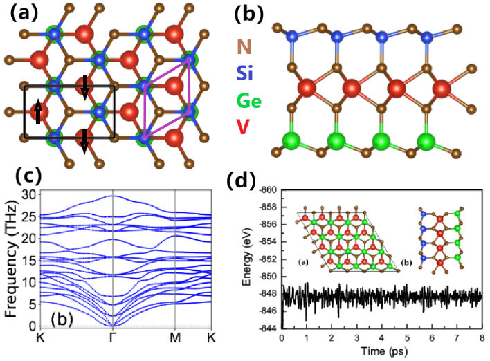
As shown in Figure 1, this structure of monolayer is stacked by seven atomic layers of N-Si-N-V-N-Ge-N. This can be regarded as a sandwich structure, and the middle layer is sandwiched by SiN and GeN bilayers, which can be considered as a Janus structure. The monolayer can be built by replacing the Si/Ge atoms of one of two SiN/GeN bilayers in / monolayer with Ge/N atoms. The symmetry of (No.156) is lower than that of / (No.187) due to the lack of the reflection symmetry with respect to the middle layer. The rhombus primitive cell and the rectangle supercell are plotted in Figure 1 (a) along with AFM configuration, and the first BZ with high-symmetry points is shown in FIG.2 of ESI. The optimized lattice constants of monolayer is 2.959 with FM ordering, which agrees well with previous theoretical value (2.97)a15 .
Our calculations show that stabilizes into a FM ground state, and the FM state is 125.7 meV lower in energy than its AFM state with rectangle supercell. The MAE includes two main termsre1 ; re2 ; re3 ; re4 : (1) MCA energy (), which is induced by the SOC, and (2) MSA energy (), which is due to the dipole-dipole (D-D) interaction:
| (1) |
where the represents the local magnetic moments and are vectors that connect the sites and . The is calculated from a energy difference between in-plane magnetization and out-of-plane magnetic anisotropy within SOC. The calculated of is only -3 . For most materials, the magnetic D-D interaction is small compared with the MCA interaction. However, for , it may play an important role due to very small . According to Equation 1, the is calculated from a energy difference with the magnetization rotating from the in-plane direction to the out-of-plane direction. The calculated is -17 , which dominates the MAE (-20 ). The positive/negative MAE means that the easy magnetization axis is perpendicular/parallel to the plane of monolayer. The calculated MAE indicates in-plane easy magnetization, which means that there is no energetic barrier to the rotation of magnetization in the planere5 . So, the can be considered as a 2D magnetre5 ; re5-1 . For a 2D XY magnet with a typical triangle lattice structure, a Berezinskii-Kosterlitz-Thouless magnetic transition to a quasi-long-range phase will produce at a critical temperature. The Monte Carlo simulations have predicted the critical temperature re6 ; re7 , where is the nearest-neighboring exchange parameter and is the Boltzmann constant. The is determined from the energy difference between AFM () and FM (). Based on the FM and AFM configurations, the AFM and FM energies can be obtained by equations:
| (2) |
| (3) |
where is the total energy of systems without magnetic coupling, and describes the easy-axis single-ion anisotropy. The corresponding can be attained:
| (4) |
The calculated is 31.43 meV (), and the is estimated to be 487 K.
The dynamical stability of is verified by its phonon band dispersion, which is presented in Figure 1 (c). Phonon branches show no imaginary frequencies, indicating the dynamical stability of . Ab initio molecular dynamics (AIMD) simulations are further performed to examine the thermal stability of on a 441 supercell with a Nose thermostat of 300 K and a step time of 1 fs. As shown in Figure 1 (d), during the 8 ps simulation time, the energy are fluctuated around the equilibrium values without any sudden changes with small distortions in the final configurations, indicating its good thermal stability. The has two independent elastic constants of and . If they satisfy Born criteria of and ela ; ela1 , the will be mechanically stable. The calculated two independent elastic constants of are =434.15 and =125.39 , which satisfy the Born criteria of mechanical stability, confirming its mechanical stability.
IV electronic structures
The magnetic anisotropy has crucial effects on the electronic states of 2D materialsa4 ; a5 ; a6 ; a7 . It is well known that the magnetization is a pseudovector. And then, the out-of-plane FM breaks all possible vertical mirrors of the system, but preserves the horizontal mirror symmetry. The preserved horizontal mirror symmetry allows the spontaneous valley polarization and a nonvanishing Chern number of a 2D systema4 . Although the magnetocrystalline direction of monolayer is in-plane, this can be easily regulated into out-of-plane by external magnetic field due to the very small MAE.
For monolayer, the spin-polarized band structures by using both GGA+ and GGA++SOC are shown in Figure 2. Figure 2 (a) shows a distinct spin splitting due to the exchange interaction, and is a direct narrow band gap semiconductor with gap value of 0.242 eV. The valence band maximum (VBM) and conduction band bottom (CBM) are at K/-K point, which are provided by the spin-up. The energies of -K and K valleys are degenerate for both conduction and valence bands. The V- orbitals lie in a trigonal prismatic crystal field environment, and the orbitals split into low-lying orbital, + and + orbitals. According to projected band structure in FIG.3 of ESI, only top -dominated valence band in spin-up direction is occupied by one electron. This is expected to lead to a magnetic moment of the 1 for each V atom, which conforms to the calculated value of 1.1 .
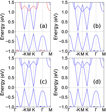
When including SOC, the valley polarization can be induced with out-of-plane magnetic anisotropy, as shown in Figure 2 (b). The valley splitting of bottom conduction band is 67 meV, while the valley splitting of top valence band is only 2 meV. For bottom conduction band, the energy of K valley is higher than that of -K valley. As plotted in Figure 2 (c), the valley polarization can be switched by reversing the magnetization direction (The energy of -K valley is higher than one of K valley.). Figure 2 (b) and (c) show that the gap value of is about 0.10 eV. Based on Figure 2 (d), no valley polarization can be observed with in-plane magnetic anisotropy, and it is still a direct band gap semiconductor (0.134 eV).
FIG.3 of ESI show that the +/ orbitals dominate -K and K valleys of bottom conduction band/top valence band, which determines the strength of valley splitting. The intra-atomic interaction from SOC mainly gives rise to valley polarization, which with out-of-plane magnetization can be expressed asf6 ; v2 ; v3 :
| (5) |
where / is the orbital angular moment along direction/coupling strength. The resulting energy of K or -K valley can be written as:
| (6) |
where (subscript as valley index) means the orbital basis for -K or K valley. If + orbitals dominate -K and K valleys, the valley splitting can be written as:
| (7) |
If the -K and K valleys are mainly from orbitals, the valley splitting is written as:
| (8) |
According to FIG.3 of ESI, the valley splitting of bottom conduction band will be very large, and the valley splitting of top valence band will be very small, which agree well with our calculated results. With general magnetization orientation, v3 (=0/90∘ denotes out-of-plane/in-plane direction.) for +-dominated -K/K valley. For in-plane one, the valley splitting of will be zero.
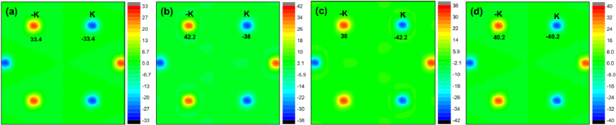
When an in-plane longitudinal electric field is applied, Bloch electrons can attain anomalous velocity , which is associated with Berry curvature :q9 . The calculated Berry curvature of as a contour map in 2D BZ with and without SOC are plotted in Figure 3, and their hot spots are around -K and K valleys. The four situations all show that Berry curvatures have opposite signs around -K and K valleys with equal/unequal magnitudes for valley-nonpolarized/valley-polarized situation. When reversing the magnetization from to direction, the signs of Berry curvature at -K and K valleys remain unchanged, but their magnitudes exchange to each other. When the Fermi level falls between the -K and K valleys with appropriate electron doping, the Berry curvature forces the spin-up carriers of K valley to accumulate on one side of the sample by an applied in-plane electric field, giving rise to an anomalous valley Hall effect (AVHE). When the magnetization is reversed, the spin-down carriers of -K valley move to another side of the sample due to opposite Berry curvature compared with one of K valley.
V strain effects
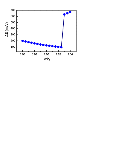
Strain is an effective method to tune the electronic state of some 2D materials, and can produce novel electronic states, such as FV, QAH and HVM statesa7 ; a9 ; a10 . We use to simulate the biaxial strain, where / are the strained/unstrained lattice constants. Here, both compressive (1) and tensile (1) strains are applied to achieve electronic states tuning(:0.961.04). As shown in Figure 4, the total energy differences between AFM and FM ordering by using rectangle supercell indicate that the FM state is always the magnetic ground state of in considered strain range. It is found that total energy differences between AFM and FM ordering at =1.03 has a sudden jump. To explain this, the energies of AFM and FM ordering as a function of are plotted in FIG.4 of ESI. Calculated results show that the energy of AFM ordering suddenly increases at =1.03. To further reveal the underlying causes, the magnetic moments of V atom for both AFM and FM ordering as a function of are plotted in FIG.5 of ESI. The energy difference jump is due to an abrupt change of the magnetic moment of V atom for AFM ordering, which reduces the magnetic interaction energy.
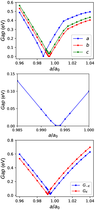
Next, the strain effects on electronic structures of are investigated. Firstly, the total energy band gaps as a function of without SOC are plotted in Figure 5, and energy band structures at some representative values are shown in FIG.6 of ESI. When the changes from 0.96 to 1.04, the gap firstly closes at about =0.987, and then continues to increase. Before the energy gap closes, is a direct gap semiconductor with VBM (CBM) at K/-K point. When 0.987, is still a direct gap semiconductor at small . When 1.01, is an indirect gap semiconductor. The CBM is at the K/-K point, whereas the VBM deviates slightly from point. In considered strain range, the K and -K valleys are always provided by the spin-up.
When including SOC, the magnetic anisotropy has crucial effects on electronic structures of . Firstly, we consider that the magnetocrystalline direction of is along out-of-plane. At some representative values, the energy band structures with GGA++SOC are plotted in FIG.7 of ESI, and the evolutions of total energy band gap along with those at -K/K point vs are shown in Figure 5. Calculated results show that there are two points around about 0.9925 and 0.9945, where the total energy band gap is closed. At the two strain points, conduction electrons are intrinsically 100% valley polarized, and the HVM state can be realizedq10 . At about 0.9925, the band gap of K valley gets closed, while a band gap at -K valley can be observed. At about 0.9945, the band gap at -K valley is zero, while the band gap of K valley is kept. The considered strain () region can be divided into three parts by two HVM electronic states.
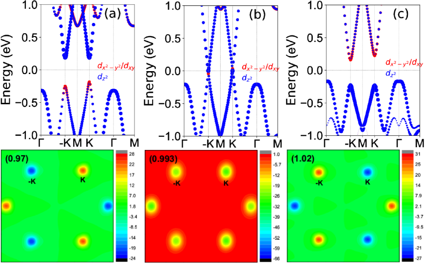
It is found that K and -K valleys of both valence and conduction bands are primarily contributed by the + or orbitals of V atoms, and the orbital characters energy band structures at representative 0.97, 0.993 and 1.02 from three regions are plotted in Figure 6. For 0.960.9925, the + orbitals dominate K and -K valleys of valence bands, while the two valleys of conduction bands are mainly from orbitals (For example 0.97). When is between 0.9925 and 0.9945, the +/ orbitals dominate K valleys of conduction/vallence bands, while orbital characters of -K valley remain unchanged (For example 0.993). For 0.99451.04, the distributions of + and orbitals are opposite to ones of 0.960.9925 (For example 1.02). These mean that there are two-time band inversion between + and orbitals with increasing . The first occurs at K valley, accompanied by the first HVM state. The second band inversion occurs at -K valley, along with the second HVM state.
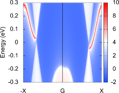
The two HVM states imply that the total gap of closes and reopens two times, which suggests topological phase transition along with band inversion between + and orbitals. The QAH state may appear, when is between 0.9925 and 0.9945. The edge states at representative 0.993 are calculated to confirm QAH phase, which is plotted in Figure 7. It is clearly seen that a nontrivial chiral edge state connects the conduction bands and valence bands, implying a QAH phase. The calculated Chern number =-1, which is also obtained by integrating the Berry curvature (see Figure 6) within the first BZ. There are no nontrivial chiral edge states for the other two regions (0.960.9925 and 0.99451.04). With increasing , two-time topological phase transitions can be observed in monolayer .
The transformations of Berry curvatures of K and -K valleys are related with these topological phase transitions, and the distributions of Berry curvature are plotted in Figure 6 at representative 0.97, 0.993 and 1.02. For 0.960.9925 and 0.99451.04, the Berry curvatures around -K and K valleys have the opposite signs and different magnitudes. However, for 0.99250.9945, the same signs and different magnitudes can be observed for Berry curvatures around -K and K valleys. When changes from 0.96 to 1.04, there are twice topological phase transitions, which are related the flipping of the sign of Berry curvature at -K or K valley. For the first topological phase transitions, the positive Berry curvature (0.97) changes into negative one (0.993) at K valley. The second topological phase transition is related with the sign flipping of Berry curvature of -K valley, and the negative Berry curvature (0.993) changes into positive one (1.02). These suggest that strain can induce sign-reversible Berry curvature at K or -K valley, and this is relevant to topological phase transition.
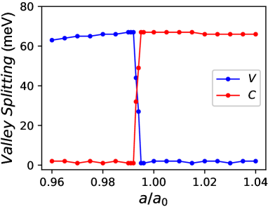
Calculated results show that monolayer has spontaneous valley polarization, and the valley splitting for both valence and condition bands is plotted in Figure 8. For 0.960.9925, the valley splitting of valence band is noteworthy, while the valley splitting of conduction band is very small. However, for 0.99451.04, the opposite situation can be observed for valley splitting, compared with the case of 0.960.9925. These can be explained by the distributions of + and orbitals (see Figure 6). If +/ orbitals dominate -K and K valleys, the valley splitting will be large/small. For 0.99250.9945, the valley splitting for both valence and condition bands is observable. In this region, is a VQAHI with spontaneous valley splitting and chiral edge states. For VAQHI, the edge state has a special behavior of chiral-spin-valley locking. For example 0.993, the edge state in Figure 7 is spin up with 100% spin polarization and 100% valley polarization, which is because the bands near the Fermi level are dominated by spin-up bands . The edge state only appears at the K valley due to the flipping of the sign of the Berry curvature or band inversion at K valley. When the magnetization is reversed, the edge state will move to the -K valley with an opposite spin direction and chiral.
In quick succession, we suppose the magnetocrystalline direction of monolayer along in-plane one. The energy band gaps as a function of are plotted in Figure 5, and the representative energy band structures are shown in FIG.8 of ESI. When changes from 0.96 to 1.04, the gap firstly decreases, and then increases. The corresponding of gap close is about 0.993. It is found that no spontaneous valley polarization in both valence and conduction bands can be observed, and no QAH phase can be induced by strain. When is less than about1.01 except 0.993 (semimetal), is a direct gap semiconductor with VBM (CBM) at K/-K point. When 1.01, is s an indirect gap semiconductor with CBM at the K/-K points, and the VBM deviates slightly from point. In short, monolayer is a common FM semiconductor or semimetal.
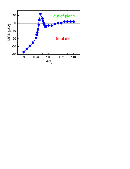
Finally, we investigate the strain effects on MAE of . We plot the MCA energy as a function of in Figure 9. Strain-driven complex MCA (multiple transitions in the MCA) can be observed. In considered strain range, the MSA energy changes from -19 to -17 to -15 , when the changes from 0.96 to 1.00 to 1.04. Calculated results show that the MAE is always negative within considered strain range, which means that strained is intrinsically common magnetic semiconductor. However, the magnetization can be adjusted from the in-plane to off-plane direction through overcoming a small energy barrier by the external magnetic field, which will produce valley polarization and QAH phase. Within considered strain range, the largest energy barrier (56 at =0.96) is equivalent to applying a external magnetic field of around 0.28-0.56 T.
VI Discussion and Conclusion
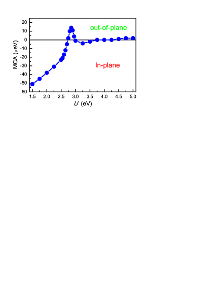
Monolayer shows the same electronic states induced by strain with for both out-of-plane and in-plane casesa7 . However, the MCA energy of varies monotonously with increasing . The strain can suppress/enhance the kinetic energy of electron, and then effectively enhances/suppresses the correlation effecta5 . This means that electronic correlation can induce the similar change of electronic states and MCA energy with strain, which has been confirmed for a7 . To further confirm complex strain dependence of MCA energy, we calculate the MCA energy as a function of correlation strength , which is also plotted in Figure 9. It is clearly seen that the MCA vs and MCA vs show very similar behavior, as expected. The complex strain dependence of MCA can be readily extended to , , and so on, because they share the same crystal structure with . In fact, for , one can observe similar transitions in the MCA energy as a function of a5 .
In summary, we have demonstrated that strain can result in a different phase diagram for different magnetic anisotropy (out-of-plane and in-plane cases). For out-of-plane situation, the strain can induce novel VQAHI with exotic chiral-spin-valley locking edge states between two HVM states, and these are related with sign-reversible Berry curvature and band inversions of + and orbitals at -K and K valleys. For in-plane situation, is a common magnetic semiconductor without spontaneous valley polarization. Particularly, the calculated intrinsic MCA energy shows multiple transitions induced by strain, which is further confirmed by calculating MCA vs . Intrinsically, there is not a VQAHI, which can be realized by external magnetic field. Our works deepen our understanding of strain effects in the V-based 2D family materials, and open new perspectives for multifunctional electronic device applications based on these materials.
Acknowledgements.
This work is supported by Natural Science Basis Research Plan in Shaanxi Province of China (2021JM-456), Graduate Innovation Fund Project in Xi’an University of Posts and Telecommunications (CXJJDL2021001). We are grateful to Shanxi Supercomputing Center of China, and the calculations were performed on TianHe-2.References
- (1) N. D. Mermin and H. Wagner, Phys. Rev. Lett. 17, 1133 (1966).
- (2) C. Gong, L. Li, Z. Li, H. Ji, A. Stern, Y. Xia, T. Cao, W. Bao, C. Wang, Y. Wang, Z. Q. Qiu, R. J. Cava, S. G. Louie, J. Xia and X. Zhang, Nature 546, 265 (2017).
- (3) B. Huang, G. Clark, E. Navarro-Moratalla, D. R. Klein, R. Cheng, K. L. Seyler, D. Zhong, E. Schmidgall, M. A. McGuire, D. H. Cobden, W. Yao, D. Xiao, P. Jarillo-Herrero and X. Xu, Nature 546, 270 (2017).
- (4) X. Liu, H. C. Hsu, and C. X. Liu, Phys. Rev. Lett. 111, 086802 (2013).
- (5) S. Li, Q. Q. Wang, C. M. Zhang, P. Guo and S. A. Yang, Phys. Rev. B 104, 085149 (2021).
- (6) S. D. Guo, J. X. Zhu, M. Y. Yin and B. G. Liu, Phys. Rev. B 105, 104416 (2022).
- (7) S. D. Guo, W. Q. Mu and B. G. Liu, 2D Mater. 9, 035011 (2022).
- (8) S. Yang, Y. Chen and C. Jiang, InfoMat. 3, 397 (2021).
- (9) Y. L. Wang and Y. Ding, Appl. Phys. Lett. 119, 193101 (2021).
- (10) H. Huan, Y. Xue, B. Zhao, G. Y. Gao, H. R. Bao and Z. Q. Yang, Phys. Rev. B 104, 165427 (2021).
- (11) Y. L. Hong, Z. B. Liu, L. Wang T. Y. Zhou, W. Ma, C. Xu, S. Feng, L. Chen, M. L. Chen, D. M. Sun, X. Q. Chen, H. M. Cheng and W. C. Ren, Science 369, 670 (2020).
- (12) L. Wang, Y. Shi, M. Liu, A. Zhang, Y.-L. Hong, R. Li, Q. Gao, M. Chen, W. Ren, H.-M. Cheng, Y. Li, and X.- Q. Chen, Nature Communications 12, 2361 (2021).
- (13) Q. Wang, L. Cao, S. J. Liang et al., npj 2D Mater. Appl. 5, 71 (2021).
- (14) L. Cao, G. Zhou, Q. Wang L. K. Ang and Y. S. Ang, Appl. Phys. Lett. 118, 013106 (2021).
- (15) S. D. Guo, W. Q. Mu, Y. T. Zhu, R. Y. Han and W. C. Ren, J. Mater. Chem. C 9, 2464 (2021).
- (16) S. D. Guo, Y. T. Zhu, W. Q. Mu and X. Q. Chen, J. Mater. Chem. C 9, 7465 (2021).
- (17) D. Dey, A. Ray and L. P. Yu, arXiv:2203.11605 (2022).
- (18) P. Hohenberg and W. Kohn, Phys. Rev. 136, B864 (1964); W. Kohn and L. J. Sham, Phys. Rev. 140, A1133 (1965).
- (19) G. Kresse, J. Non-Cryst. Solids 193, 222 (1995).
- (20) G. Kresse and J. Furthmller, Comput. Mater. Sci. 6, 15 (1996).
- (21) G. Kresse and D. Joubert, Phys. Rev. B 59, 1758 (1999).
- (22) J. P. Perdew, K. Burke and M. Ernzerhof, Phys. Rev. Lett. 77, 3865 (1996).
- (23) S. L. Dudarev, G. A. Botton, S. Y. Savrasov, C. J. Humphreys and A. P. Sutton, Phys. Rev. B 57, 1505 (1998).
- (24) A. Togo, F. Oba, and I. Tanaka, Phys. Rev. B 78, 134106 (2008).
- (25) T. Fukui, Y. Hatsugai and H. Suzuki, J. Phys. Soc. Japan. 74, 1674 (2005).
- (26) H. J. Kim, https://github.com/Infant83/VASPBERRY, (2018).
- (27) H. J. Kim, C. Li, J. Feng, J.-H. Cho, and Z. Zhang, Phys. Rev. B 93, 041404(R) (2016).
- (28) A. A. Mostofia, J. R. Yatesb, G. Pizzif, Y.-S. Lee, I. Souzad, D. Vanderbilte and N. Marzarif, Comput. Phys. Commun. 185, 2309 (2014).
- (29) Q. Wu, S. Zhang, H. F. Song, M. Troyer and A. A. Soluyanov, Comput. Phys. Commun. 224, 405 (2018).
- (30) X. B. Lu, R. X. Fei, L. H. Zhu and L. Yang, Nat. Commun. 11, 4724 (2020).
- (31) M. Akram, H. LaBollita, D. Dey, J. Kapeghian, O. Erten and A. S. Botana, Nano Lett. 21, 6633 (2021).
- (32) H. J. F. Jansen, Phys. Rev. B 59, 4699 (1999).
- (33) F. Xue, Y. Hou, Z. Wang and R. Wu, Phys. Rev. B 100, 224429 (2019).
- (34) K. Sheng, Q. Chen , H. K. Yuan and Z. Y. Wang, Phys. Rev. B 105, 075304 (2022).
- (35) J. L. Lado and J. Fernndez-Rossier, 2D Mater. 4, 035002 (2017).
- (36) P. Jiang, L. Kang, Y.-L. Li, X. Zheng, Z. Zeng, and S. Sanvito, Phys. Rev. B 104, 035430 (2021).
- (37) S. Zhang, R. Xu, W. Duan, and X. Zou, Adv. Funct. Mater. 29, 1808380 (2019).
- (38) E. Cadelano and L. Colombo, Phys. Rev. B 85, 245434 (2012).
- (39) Y. X.Wu, W. Sun, S. Y. Liu, B. Wang, C. Liu, H. B. Yin and Z. X. Cheng, Nanoscale 13, 16564 (2021).
- (40) W. Y. Tong, S. J. Gong, X. Wan, and C. G. Duan, Nat. Commun. 7, 13612 (2016).
- (41) P. Zhao, Y. Dai, H. Wang, B. B. Huang and Y. D. Ma, ChemPhysMater, 1, 56 (2022).
- (42) R. Li, J. W. Jiang, W. B. Mi and H. L. Bai, Nanoscale 13, 14807 (2021).
- (43) D. Xiao, M. C. Chang, and Q. Niu, Rev. Mod. Phys. 82, 1959 (2010).
- (44) H. Hu, W. Y. Tong, Y. H. Shen, X. Wan, and C. G. Duan, npj Comput. Mater. 6, 129 (2020).