Thermal transport in nanoelectronic devices cooled by on-chip magnetic refrigeration
Abstract
On-chip demagnetization refrigeration has recently emerged as a powerful tool for reaching microkelvin electron temperatures in nanoscale structures. The relative importance of cooling on-chip and off-chip components and the thermal subsystem dynamics are yet to be analyzed. We study a Coulomb blockade thermometer with on-chip copper refrigerant both experimentally and numerically, showing that dynamics in this device are captured by a first-principles model. Our work shows how to simulate thermal dynamics in devices down to microkelvin temperatures, and outlines a recipe for a low-investment platform for quantum technologies and fundamental nanoscience in this novel temperature range.
Easy access to millikelvin temperatures has driven the expansion of quantum research and technologies for the past decade. Understanding microkelvin physics has the potential to become the next field-defining development. Until recently, the lowest electron temperature reached by external refrigeration in micro- and nanoelectronic devices was Xia et al. (2000); Samkharadze et al. (2011); Bradley et al. (2016); Jones et al. (2020). Electrons in bulk metals are routinely cooled to much lower temperatures by nuclear demagnetization refrigeration, but the thermal coupling to a device via an insulating structure vanishes rapidly as temperature approaches the microkelvin regime. This limitation to reaching microkelvin on-chip electron temperatures has recently been overcome using two different approaches: cooling of metallic contacts by immersion in 3He Levitin et al. (2022) and incorporation of miniaturized on-chip demagnetization elements Bradley et al. (2017); Palma et al. (2017); Yurttagül et al. (2019). In combination with demagnetization cooldown of all external structures in direct contact with the target device, the latter approach has produced on-chip demagnetization with hours of hold time at microkelvin temperatures Sarsby et al. (2020); Samani et al. (2022). However, the simultaneous demagnetization of multiple coolants makes it challenging to gain insight into subsystem temperatures that cannot be directly measured, hiding the dynamic details from view. Traditional bulk demagnetization infrastructure can also be prohibitively voluminous and expensive for many applications.
In this Article, we investigate a minimalist copper on-chip demagnetization system in a helium-bath dilution refrigerator. We report the coldest on-chip-only demagnetization cooldown experiment to date, reaching a device electron temperature mK. The demagnetization dynamics are well captured by a first-principles thermal model, enabling analysis and predictions beyond experimental limitations. We show that the demagnetization base temperature and hold time are determined by the heat leak carried by the substrate phonons, originating from the grounded metal layer under the substrate. We predict that holding the metal layer at a manageable would allow reaching hours of hold time at microkelvin temperatures. Perhaps surprisingly, this can also be achieved with “hot” electrical connections to the demagnetization island or, alternatively, a contact resistance as low as . We also predict that engineering the substrate to optimize the phonon heat leak allows achieving microkelvin on-chip temperatures even in a commercial cryostat.
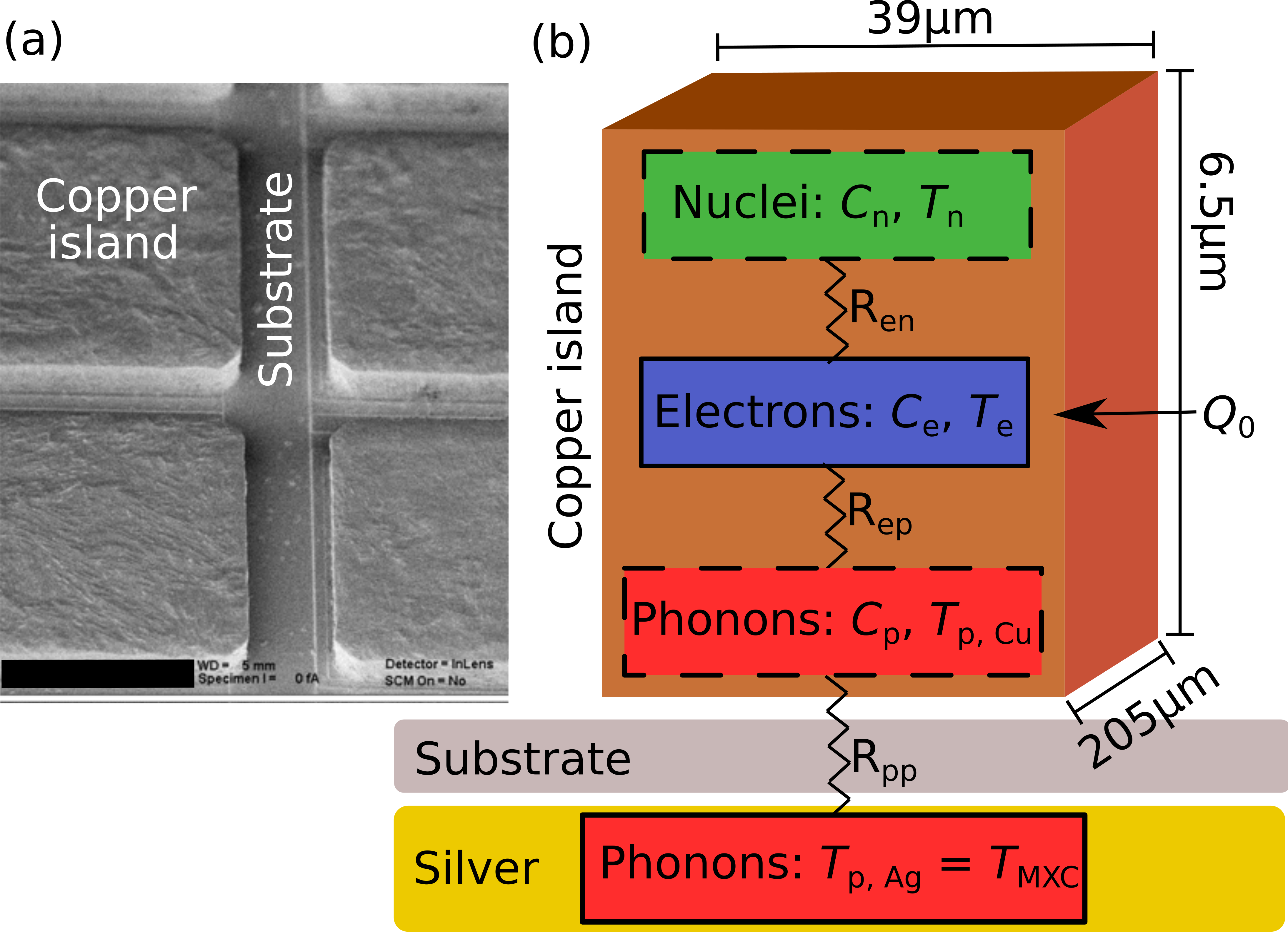
We study the on-chip demagnetization process using devices consisting of copper islands as illustrated in Fig. 1a. The islands are attached to a layered substrate (see SM_ ), placed on an underlying silver platform. The silver platform is well thermalized to the mixing chamber of the dilution refrigerator at temperature via silver sinters Franco et al. (1984); Autti et al. (2020). Thus, the phonon temperature in the silver layer . is measured directly using a vibrating wire thermometer immersed in the liquid 3He/4He mixture Bradley and Oswald (1990); Pentti et al. (2011). The copper contains three independent thermal reservoirs, phonons at temperature , electrons at temperature , and nuclear spins at . The phonon and nuclear temperatures cannot be directly measured. The electron temperature in an array of such copper islands, connected by tunnel junctions, can be measured in-situ by operating the device as a Coulomb Blockade Thermometer (CBT) Pekola et al. (1994). Each CBT tunnel junction resistance is of the order of , as required for the operation of the CBT. This means that the tunnel junctions do not provide a significant thermal link between adjacent islands and the array can thermally be described as a collection of isolated copper islands, as shown in Fig. 1b.
The experimental results described below were obtained from two different CBTs with on-chip copper refrigerant. Both were made following the same design and fabrication process as in our previous studies Bradley et al. (2016, 2017); Prunnila et al. (2010). The first device is a “junction CBT” (jCBT), meaning that the island capacitance is dominated by the capacitance of the tunnel junctions between islands. For the second device, the capacitance of the metal islands was increased by a factor of roughly by coating the islands with a dielectric layer followed by a layer of metal Samani et al. (2022). This reduces the island charging energy and enables operation down to at least Samani et al. (2022). CBT devices where the capacitance of each island is dominated by its capacitance to a gate electrode or ground rather than by its coupling to neighboring islands are referred to as “gate CBTs” (gCBT) Samani et al. (2022). After calibration as a function of bias voltage, the CBT electron temperature can be inferred from the zero-bias differential conductance of the device as detailed in SM_ .
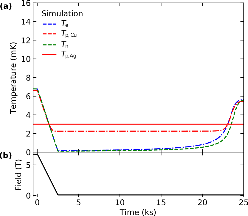
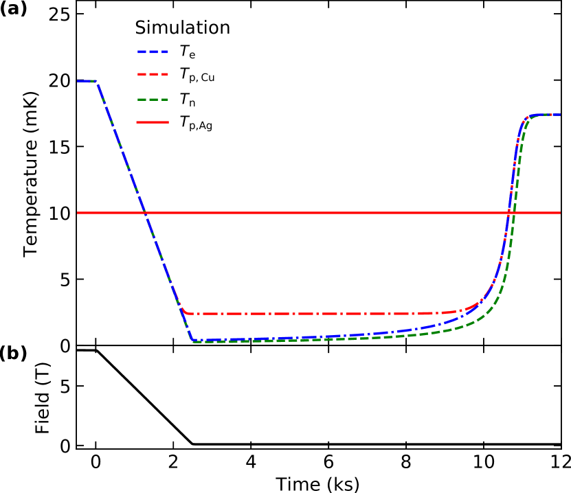
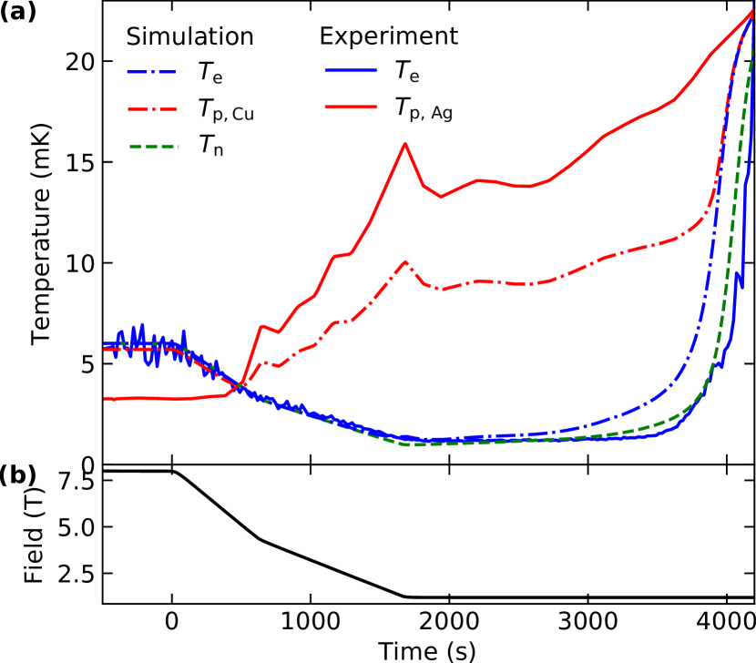
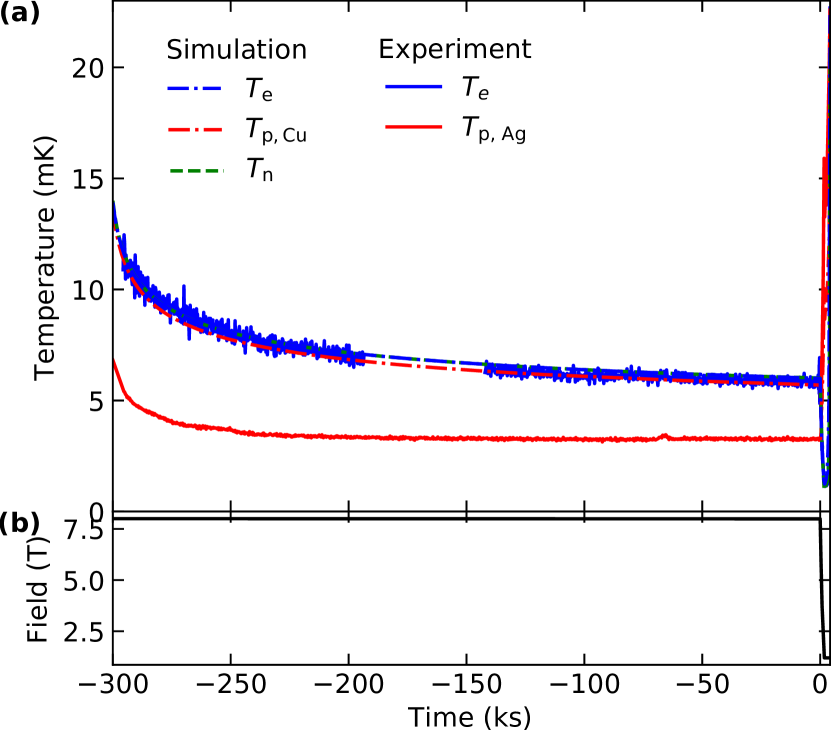
Using nuclear demagnetization cooling, the CBT islands can be cooled to temperatures below those reachable by continuous cooldown. Demagnetization experiments start by ramping the magnetic field to its maximum value (here T), and then waiting for the dilution refrigerator and the CBT’s electrons to thermalize. After a few days, the CBT electrons reach their equilibrium temperature , and the mixing chamber temperature stabilizes at mK. The data measured using the gate CBT, shown in Figure 2, starts in this pre-cooled configuration. The pre-cooling is shown in Fig. S4 in SM_ .
The entropy of the nuclear system is purely a function of . For an ideal adiabatic demagnetization process this ratio remains constant Pobell (2007), causing to decrease proportional to the change in the field magnitude. Copper electrons are then cooled via the coupling between the electrons and the nuclei. After the pre-cooling, the field is swept down to T while recording the zero bias conductance of the CBT and continuously adjusting the DC bias to ensure zero bias is maintained. The minimum measured electron temperature reached in Fig. 2 is mK. Systematic uncertainties in the measured temperatures are discussed in SM_ , while measurement noise is insignificant at mK due to narrowing of the CBT conductance dip.
We simulate the subsystem temperature evolution in a single copper island. The copper nuclear temperature is assumed to change adiabatically as a function of . The nuclear, electron, and phonon temperatures then evolve as determined by their associated temperature-dependent heat capacities and couplings, and according to associated heat leaks to the electrons and phonons (see Fig. 1b). The parameter values and functional dependencies are taken from literature Jones et al. (2020). Additionally, the estimated total Kapitza resistance through the layered substrate, , agrees with the values extracted from the pre-cooling data for each CBT device. All these aspects are detailed and substantiated in SM_ .
The temperature difference between the mixing chamber and the copper electrons at the end of the pre-cooling corresponds to a constant heat leak of to the electron system. This is used as an input parameter for the demagnetization simulation. This heat leak is likely caused by small vibrations of the CBT holder in the magnetic field, resulting in eddy current heating Todoshchenko et al. (2014) when the full magnetic field is applied. This means that probably decreases when the field is decreased, but we ignore that for simplicity. Even in the absence of any heat leak the electron temperature would only very slowly decrease below during the pre-cooling because the nuclear heat capacity is very large in T.
The simulation shown in Fig. 2 starts at ks, first replicating three days of pre-cooling data (Fig. S4). The demagnetization is simulated from the initial state obtained this way. During the demagnetization, the weakening thermal link between phonons and electrons allows the electrons to be cooled below the phonon temperature. Eddy currents generated in the refrigerator support structures heat up the mixing chamber with a delay, leading to increasing . The copper phonons are kept at an elevated temperature by the heat leak via . The simulated during the demagnetization is in nearly perfect agreement with the experiment. After about 2000 s at the final magnetic field, the electron temperature starts to increase rapidly. Remarkably, the simulation replicates this hold time within s and attributes it to the integrated heat leak from the substrate phonons. This justifies the assumption that the heat transport through the layered substrate is described by the combined Kapitza resistance . Note that if we simulate the CBT demagnetization adding mK to so that mK at the end of the pre-cooling and mK at the end of the demagnetization, the hold time is halved. On the other hand, changing by 50% does not significantly change the simulation outcome (see SM_ ). That is, the exact value of unimportant and, instead, the temperature difference across the substrate defines the resulting heat transport. Note also that plays no role in determining the hold time. Therefore, the thermal subsystem temperatures evolve as predicted by first-principles expressions in this novel temperature range.
The minimum is determined by the balance of the phonon heat leak against the coupling between the nuclei and electrons. The electron-nuclei heat flow does not increase significantly if the nuclei are made yet colder. If we continue the demagnetization below 1.2 T, there is practically no improvement in the minimum reached in either the simulation or the experiment owing to the substrate heat leak.
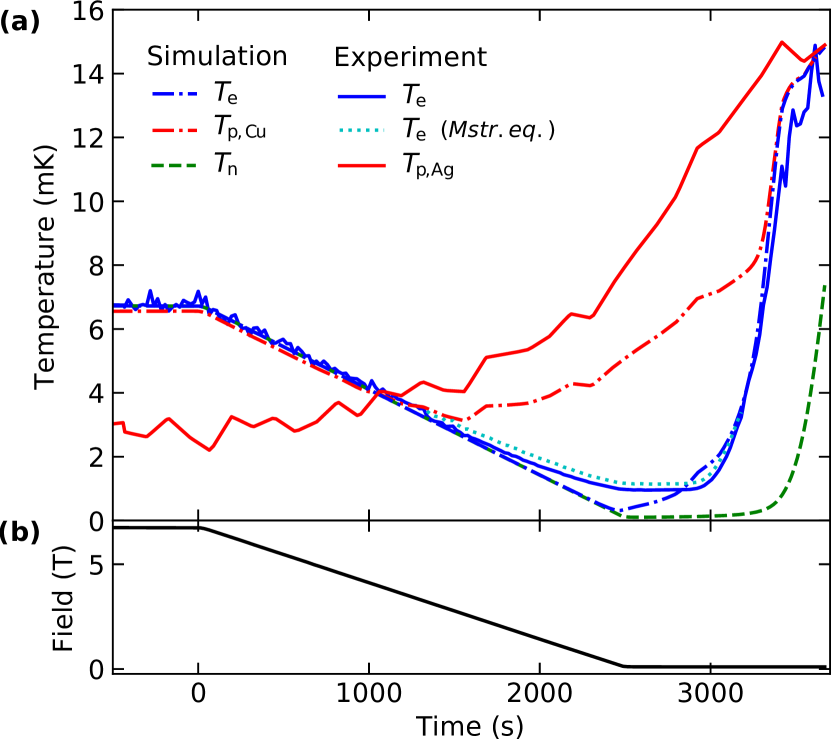
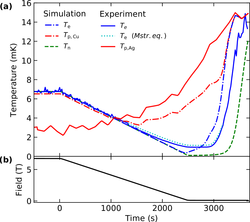
We can mitigate the dynamic increase in by starting from a lower initial T. Here we used a "junction" CBT, which loses sensitivity to electron temperature below mK (see SM_ ), but has a larger Kapitza resistance and is thus better protected from the substrate heat leak. This allows us to ramp the field down to mT to extract all cooling capacity from the nuclei. The experimental outcome is compared with a simulation in Fig. 3.
The lowest measured CBT electron temperature is mK. This reading is caused by the AC excitation used to read out the zero-bias conductance of the device as explained in SM_ . In the simulation, the minimum electron temperature is . It thus seems likely that also the experiment cools well into the microkelvin temperature regime, but obtaining conclusive evidence requires using a device where such readout limitations are absent. We note that while the gCBT design removes this issue, the resulting reduction in the Kapitza resistance makes microkelvin temperatures harder to reach with elevated phonon temperatures. The hold time in the junction CBT measurement is reduced as compared with Fig. 2 because the nuclear heat capacity is proportional to . That is, the simulation reproduces the experimental data nearly perfectly where the experimental data is reliable. Combining this with the analysis of the gate CBT, we conclude that the simulation model can be used to predict the dynamic demagnetization performance in conditions yet beyond experimental reach, and not only where the predicted hold time is long or the substrate temperature stable.
The only relevant heat leak contribution is that carried by the substrate phonons. If we fix the silver layer phonon temperature in the simulation to 3 mK as shown in Fig. 4, a demagnetization otherwise identical to that in Fig. 3 results in a minimum electron temperature of and a hold time of several hours under 1 mK. The hold time in this configuration is limited by , which is likely to decrease when is reduced owing to decreased eddy current heating in the CBT. Note that electronic heat conductivity along the electric connection to the demagnetization islands (resistance ) is negligible assuming the wiring is at the same temperature as the silver platform. This implies that external demagnetization to cool the electrons in the wiring Sarsby et al. (2020); Samani et al. (2022) should not be necessary for reaching microkelvin device temperatures.
The 3 mK silver layer temperature could be achieved by optimizing the performance of the dilution refrigerator, by replacing the silver layer with copper that will demagnetize alongside the CBT, or by using a sub-mK refrigerator platform Nyéki et al. (2022); Schmoranzer et al. (2020). However, if we increase the Kapitza resistance by two orders of magnitude as discussed in the Supplemental Material (Fig. S6), sub-mK electron temperatures can be achieved even if the substrate can only be cooled to 10 mK. This would allow low-investment access to sub-mK temperatures even in a commercial cryogen-free dilution refrigerator.
The on-chip cooldown performance and thermal dynamics of diverse new devices can be predicted using the simulation techniques presented in this Letter. For example, the electric contact resistance to the demagnetized metal could be lowered to without compromising the demagnetization performance, provided the electron temperature of the wiring is kept at 3 mK. Low contact resistances are essential in studying for example two-dimensional electron gases in semiconductors, nanomechanical resonators, and quantum circuits, all of which have previously been subjected to microkelvin bulk cooling techniques Cattiaux et al. (2021); Lane et al. (2020); Levitin et al. (2022). On-chip refrigeration could allow access to temperatures deep in the microkelvin regime in devices like these using only a standard dilution refrigerator platform. We emphasize that the technique can be used to cool also phonons in the materials in contact with the demagnetization metal. Thus, on-chip magnetic refrigeration can be applied to a broad range of devices for the purposes of novel fundamental nanoscience and quantum technologies.
Acknowledgements.
All the data in this Letter are available at https://doi.org/10.17635/lancaster/researchdata/xxx, including descriptions of the data sets. The simulation codes can be obtained from the corresponding author upon reasonable request. This research is supported by the U.K. EPSRC (EP/K01675X/1, EP/N019199/1, EP/P024203/1, EP/L000016/1, and EP/W015730/1), the European FP7 Programme MICROKELVIN (228464), the European Union’s Horizon 2020 research and innovation programme (European Microkelvin Platform 824109, and EFINED 766853), by the Academy of Finland through the Centre of Excellence program (projects 336817 and 312294), and by Business Finland through QuTI-project (40562/31/2020). S.A. acknowledges financial support from the Jenny and Antti Wihuri Foundation via the Council of Finnish Foundations. M.D.T acknowledges financial support from the Royal Academy of Engineering (RF\201819\18\2).References
- Xia et al. (2000) J. S. Xia, E. D. Adams, V. Shvarts, W. Pan, H. L. Stormer, and D. C. Tsui, “Ultra-low-temperature cooling of two-dimensional electron gas,” Physica B: Cond. Mat. 280, 491–492 (2000).
- Samkharadze et al. (2011) N. Samkharadze, A. Kumar, M. J. Manfra, L. N. Pfeiffer, K. W. West, and G. A. Csáthy, “Integrated electronic transport and thermometry at milliKelvin temperatures and in strong magnetic fields,” Rev. Sci. Instr. 82, 053902 (2011).
- Bradley et al. (2016) D. I. Bradley, R. E. George, D. Gunnarsson, R. P. Haley, H. Heikkinen, Yu. A. Pashkin, J. Penttilä, J. R. Prance, M. Prunnila, L. Roschier, and M. Sarsby, “Nanoelectronic primary thermometry below 4 mK,” Nat. Commun. 7, 10455 (2016).
- Jones et al. (2020) AT Jones, CP Scheller, JR Prance, YB Kalyoncu, DM Zumbühl, and RP Haley, “Progress in cooling nanoelectronic devices to ultra-low temperatures,” J. Low Temp. Phys. 201, 772–802 (2020).
- Levitin et al. (2022) Lev V. Levitin, Harriet van der Vliet, Terje Theisen, Stefanos Dimitriadis, Marijn Lucas, Antonio D. Corcoles, Ján Nyéki, Andrew J. Casey, Graham Creeth, Ian Farrer, David A. Ritchie, James T. Nicholls, and John Saunders, “Cooling low-dimensional electron systems into the microkelvin regime,” Nat. Commun. 13, 667 (2022).
- Bradley et al. (2017) D. I. Bradley, A. M. Guénault, D. Gunnarsson, R. P. Haley, S. Holt, A. T. Jones, Yu. A. Pashkin, J. Penttilä, J. R. Prance, M. Prunnila, and L. Roschier, “On-chip magnetic cooling of a nanoelectronic device,” Sci. Rep. 7, 45566 (2017).
- Palma et al. (2017) M. Palma, C. P. Scheller, D. Maradan, A. V. Feshchenko, M. Meschke, and D. M. Zumbühl, “On-and-off chip cooling of a Coulomb blockade thermometer down to 2.8 mK,” Appl. Phys. Lett. 111, 253105 (2017).
- Yurttagül et al. (2019) N. Yurttagül, M. Sarsby, and A. Geresdi, “Indium as a high-cooling-power nuclear refrigerant for quantum nanoelectronics,” Phys. Rev. Appl. 12, 011005(R) (2019).
- Sarsby et al. (2020) Matthew Sarsby, Nikolai Yurttagül, and Attila Geresdi, “500 microkelvin nanoelectronics,” Nat. Commun. 11, 1–7 (2020).
- Samani et al. (2022) Mohammad Samani, Christian P Scheller, Omid Sharifi Sedeh, Dominik M Zumbühl, Nikolai Yurttagül, Kestutis Grigoras, David Gunnarsson, Mika Prunnila, Alexander T Jones, Jonathan R Prance, et al., “Microkelvin electronics on a pulse-tube cryostat with a gate coulomb-blockade thermometer,” Physical Review Research 4, 033225 (2022).
- (11) See Supplemental Material at [link added by publisher] for details on the numerical simulations, CBT calibration, and CBT error estimates. The supplemental material includes Refs. [26-37].
- Franco et al. (1984) H Franco, J Bossy, and H Godfrin, “Properties of sintered silver powders and their application in heat exchangers at millikelvin temperatures,” Cryogenics 24, 477–483 (1984).
- Autti et al. (2020) S. Autti, A. M. Guénault, A. Jennings, R. P. Haley, G. R. Pickett, R. Schanen, V. Tsepelin, J. Vonka, D. E. Zmeev, and A. A. Soldatov, “Effect of the boundary condition on the kapitza resistance between superfluid and sintered metal,” Phys. Rev. B 102, 064508 (2020).
- Bradley and Oswald (1990) D. I. Bradley and R. Oswald, “Viscosity of the 3He-4He dilute phase in the mixing chamber of a dilution refrigerator,” J. Low Temp. Phys. 80, 89–97 (1990).
- Pentti et al. (2011) E. Pentti, J. Rysti, A. Salmela, A. Sebedash, and J. Tuoriniemi, “Studies on helium liquids by vibrating wires and quartz tuning forks,” J. Low Temp. Phys. 165, 132 (2011).
- Pekola et al. (1994) J. P. Pekola, K. P. Hirvi, J. P. Kauppinen, and M. A. Paalanen, “Thermometry by arrays of tunnel junctions,” Phys. Rev. Lett. 73, 2903–2906 (1994).
- Prunnila et al. (2010) M. Prunnila, M. Meschke, D. Gunnarsson, S. Enouz-Vedrenne, J. M. Kivioja, and J. P. Pekola, “Ex situ tunnel junction process technique characterized by Coulomb blockade thermometry,” Journal of Vacuum Science & Technology B 28, 1026–1029 (2010).
- Yurttagül et al. (2021a) Nikolai Yurttagül, Matthew Sarsby, and Attila Geresdi, “Coulomb blockade thermometry beyond the universal regime,” J. Low Temp. Phys. 204, 143–162 (2021a).
- Yurttagül et al. (2021b) Nikolai Yurttagül, Matthew Sarsby, and Attila Geresdi, “Coulomb blockade thermometry beyond the universal regime,” Zenodo repository (2021b), 10.5281/zenodo.3831241.
- Pobell (2007) F. Pobell, Matter and methods at low temperatures, 3rd ed. (Springer-Verlag, Berlin, 2007).
- Todoshchenko et al. (2014) I. Todoshchenko, J.-P. Kaikkonen, R. Blaauwgeers, P. J. Hakonen, and A. Savin, “Dry demagnetization cryostat for sub-millikelvin helium experiments: refrigeration and thermometry,” Rev. Sci. Instr. 85, 085106 (2014).
- Nyéki et al. (2022) J Nyéki, M Lucas, P Knappová, LV Levitin, A Casey, J Saunders, H van der Vliet, and AJ Matthews, “High-performance cryogen-free platform for microkelvin-range refrigeration,” Physical Review Applied 18, L041002 (2022).
- Schmoranzer et al. (2020) David Schmoranzer, James Butterworth, Sébastien Triqueneaux, Eddy Collin, and Andrew Fefferman, “Design evaluation of serial and parallel sub-mk continuous nuclear demagnetization refrigerators,” Cryogenics 110, 103119 (2020).
- Cattiaux et al. (2021) D Cattiaux, I Golokolenov, S Kumar, M Sillanpää, L Mercier de Lépinay, RR Gazizulin, X Zhou, AD Armour, O Bourgeois, A Fefferman, et al., “A macroscopic object passively cooled into its quantum ground state of motion beyond single-mode cooling,” Nat. Commun. 12, 1–6 (2021).
- Lane et al. (2020) J. R. Lane, D. Tan, N. R. Beysengulov, K. Nasyedkin, E. Brook, L. Zhang, T. Stefanski, H. Byeon, K. W. Murch, and J. Pollanen, “Integrating superfluids with superconducting qubit systems,” Phys. Rev. A 101, 012336 (2020).
- Farhangfar et al. (1997) Sh. Farhangfar, K. P. Hirvi, J. P. Kauppinen, J. P. Pekola, J. J. Toppari, D. V. Averin, and A. N. Korotkov, “One dimensional arrays and solitary tunnel junctions in the weak Coulomb blockade regime: CBT thermometry,” J. Low Temp. Phys. 108, 191–215 (1997).
- Hirvi et al. (1995) K. P. Hirvi, J. P. Kauppinen, A. N. Korotkov, M. A. Paalanen, and J. P. Pekola, “Arrays of normal metal tunnel junctions in weak Coulomb blockade regime,” Appl. Phys. Lett. 67, 2096–2098 (1995).
- Hahtela et al. (2016) O Hahtela, E Mykkänen, A Kemppinen, M Meschke, M Prunnila, D Gunnarsson, L Roschier, J Penttilä, and J Pekola, “Traceable Coulomb blockade thermometry,” Metrologia 54, 69–76 (2016).
- Pekola et al. (2022) Jukka P Pekola, Eemil Praks, Nikolai Yurttagül, and Bayan Karimi, “Influence of device non-uniformities on the accuracy of Coulomb blockade thermometry,” Metrologia 59, 045009 (2022).
- Hirvi et al. (1996) K. P. Hirvi, M. A. Paalanen, and J. P. Pekola, “Numerical investigation of one-dimensional tunnel junction arrays at temperatures above the Coulomb blockade regime,” J. Appl. Phys. 80, 256–263 (1996).
- Feshchenko et al. (2013) A. V. Feshchenko, M. Meschke, D. Gunnarsson, M. Prunnila, L. Roschier, J. S. Penttilä, and J. P. Pekola, “Primary thermometry in the intermediate Coulomb blockade regime,” J. Low Temp. Phys. 173, 36–44 (2013).
- Wellstood et al. (1994) F. C. Wellstood, C. Urbina, and J. Clarke, “Hot-electron effects in metals,” Phys. Rev. B 49, 5942–5955 (1994).
- Viisanen and Pekola (2018) K. L. Viisanen and J. P. Pekola, “Anomalous electronic heat capacity of copper nanowires at sub-Kelvin temperatures,” Phys. Rev. B 97, 115422 (2018).
- Meschke et al. (2004) M. Meschke, J. P. Pekola, F. Gay, R. E. Rapp, and H. Godfrin, “Electron thermalization in metallic islands probed by Coulomb blockade thermometry,” J. Low Temp. Phys. 134, 1119–1143 (2004).
- Swartz and Pohl (1989) E. T. Swartz and R. O. Pohl, “Thermal boundary resistance,” Rev. Mod. Phys. 61, 605–668 (1989).
- Klitsner and Pohl (1987) T. Klitsner and R.O. Pohl, “Phonon scattering at silicon crystal surfaces,” Physical Review B 36, 6551 (1987).
- Pierson (1996) Hugh O Pierson, Handbook of refractory carbides & nitrides: properties, characteristics, processing and applications (William Andrew, 1996) p. 193.
Supplemental Material
CBT as a primary thermometer
We measure the differential conductance of the CBTs as a function of DC bias using a current driven, four terminal lock-in measurement. In the weak Coulomb blockade limit (, where is the charging energy of the islands), develops a temperature dependent conductance dip around zero bias that can be used for primary thermometry of the electron temperature in the CBT islands Pekola et al. (1994); Farhangfar et al. (1997). The electron temperature is given by the full width at half minimum of the conductance dip, , where is the number of junctions in series in the array Pekola et al. (1994). Alternatively, a master equation (ME) model of electron tunneling in the CBT can be fitted to curves measured at several temperatures Farhangfar et al. (1997); Bradley et al. (2016) to determine the characteristic tunnel junction resistance and island capacitance. From these two values, the model can then be used to convert the zero-DC-bias conductance to electron temperature. This self-calibration allows the electron temperature to be determined in “secondary mode” where only the zero-bias conductance is measured. This is faster than measuring the full conductance curve and minimizes overheating that occurs when a DC bias is applied Farhangfar et al. (1997); Bradley et al. (2016). The ME model is valid in the “universal regime”, which extends down to a conductance suppression of , where is the asymptotic conductance at high bias Samani et al. (2022). Below this temperature, the behavior of jCBTs and gCBTs diverge and both start to disagree with the ME model. Instead, a Markov chain Monte Carlo model can be used to predict the conductance Yurttagül et al. (2021a); Samani et al. (2022). The experiments described in this Letter use both CBTs in secondary mode and almost entirely in the universal regime.
CBT calibration, uncertainty and saturation
Figure S1 shows the self-calibration of the jCBT device that was used to obtain the data shown in Fig. 3 of the article. Figure S2(a) shows the self-calibration of the gCBT device that was used to obtain the data shown in Fig. 2 of the article. After calibration, the temperature of each CBT is determined by measuring its conductance at zero bias. The temperature is measured continuously during cooling experiments as the CBT is magnetised, pre-cooled, and demagnetised.
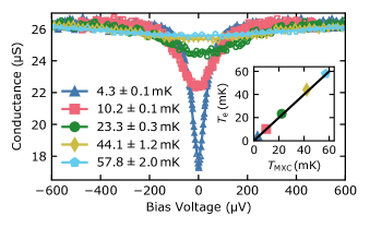
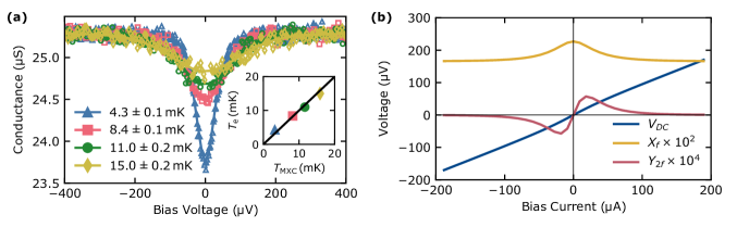
An experimental complication arises with very low temperature CBT measurements due to the narrowing of the conductance dip. For example, at our 33 junction arrays produce a conductance curve FWHM of . This means that a small DC offset of even can cause a significant pessimistic error in the measured electron temperature. To minimize this error, we track the center of the dip during the cooling process and correct any DC offset using feedback, as described in Fig. S2(b).
The intrinsic uncertainty in the temperature measured by a CBT is affected by nonuniformities in the tunnel junction resistances, tunnel junction capacitances and total island capacitances Hirvi et al. (1995); Farhangfar et al. (1997); Hahtela et al. (2016); Pekola et al. (2022). Moreover, at very low temperatures the conductance is affected by the unknown, static offset charge of each island Hirvi et al. (1996); Yurttagül et al. (2021a). For the devices studied here, the first contribution should be insignificant for the purpose of this work. The fabrication process is expected to produce very uniform tunnel junctions Prunnila et al. (2010) and the CBT uncertainty is relatively insensitive to such variations. Furthermore, for all the data shown, the CBTs are operating at sufficiently high temperatures for the effect of offset charges to be neglected. This assumption is weakest for the coldest electron temperatures shown in Fig. 3. However, using numerical results from Fig. 8 in Yurttagül et al. (2019), we have confirmed that the scale of the uncertainty due to unknown offset charges at these temperatures is small. In practice, our temperature uncertainty is dominated by two things: at higher temperatures (in the universal regime) the uncertainty of fitting parameters in the calibration for operating in secondary mode is the greatest source of uncertainty. This is the origin of the temperature uncertainties shown in Fig. S1 and Fig. S2. The same is true for uncertainties given in the main text. For the jCBT, at temperatures approaching 1 mK and below, the electron temperature measurement is also affected by the amplitude of the AC excitation used to read out the differential conductance.
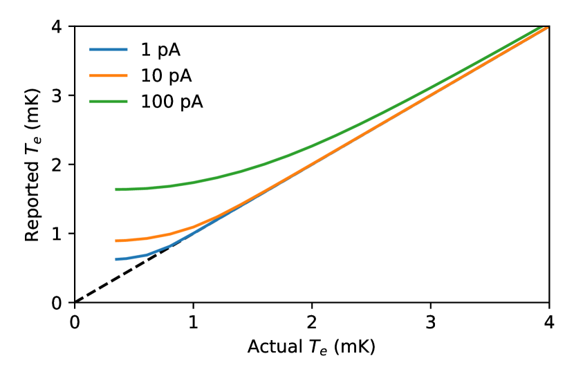
We study the uncertainty due to finite AC excitation by sampling the theoretical CBT conductance peak in the master equation model with a simulated current excitation signal. The resulting voltage signal is analyzed to find the signal at the frequency of the excitation, simulating the operation of a lock-in amplifier. The resulting conductance reading, converted to "reported" electron temperature is shown in Fig. S3. For a 10 pA excitation, as used in the experiments, the apparent electron temperature saturates around mK. This can explain the readout saturation observed in the jCBT experiment in Fig. 3. Reducing the AC current amplitude further is not possible in practice because the noise floor of the lock-in measurement would dictate an integration time that is too long for the timescale of the experiment.
The agreement between the measured and predicted electron temperatures in Fig. 3 and the results in Fig. S3 is surprisingly good, and one might be compelled to infer the actual electron temperature from conductance measurements at these temperatures by correcting for the saturation using Fig. S3. However, the master equation model is known to become increasingly unreliable at temperatures where the conductance suppression is stronger than Feshchenko et al. (2013); Yurttagül et al. (2021a). For this reason, the results in Fig. S3 cannot be used to infer the actual electron temperature in Fig. 3. Instead, the values reported in Fig. 3 represent a reliable upper limit for the electron temperature, with a lowest possible reading close to due to the AC excitation.
Simulations
The demagnetization performance of a copper island as shown in Fig. 1b of the main text is determined by the subsystem heat capacities and the thermal links between the subsystems. For the copper subsystem heat capacities we use theoretical temperature dependencies with material parameter values taken from the literature. The electron-nuclear and phonon-phonon couplings are described by first-principles expressions. The phonon-electron coupling is described by a phenomenological formula confirmed by independent prior experiments. The expressions and parameter values are explained in more detail in Ref. Jones et al. (2020).
The thermal subsystem couplings are shown in terms of thermal resistances in Fig. 1b. For numerical purposes it is however more convenient to express the couplings in terms of the heat flow between each subsystem pair.
The most important of the subsystem couplings is that controlling the heat flow between the phonons and conduction electrons Wellstood et al. (1994),
| (S1) |
where is a material specific constant ( for Cu Viisanen and Pekola (2018); Meschke et al. (2004)), and the volume of the copper island. This rapid temperature dependence allows both efficient pre-cooling of the electrons by the phonons down to a few mK and almost total thermal decoupling of the electrons from the phonons when the electrons are cooled down by the nuclei during the demagnetization.
The heat flow from the electrons to the nuclei reads
| (S2) |
Here is the molar nuclear Curie constant of copper, is the number of copper moles, is the permeability of free space, is the Korringa constant for copper with , and is the residual dipole field in copper. The copper nuclear heat capacity is defined below.
Finally, the phonon-phonon heat flow between the silver platform and the copper phonons is determined by the boundary Kapitza resistance Swartz and Pohl (1989)
| (S3) | |||||
| (S4) |
where is the contact area separating the two phonon systems, for a multi-layer metal-insulator interface as detailed in the next section, and we used the approximation that .
To simulate the subsystem temperature evolution, we also need the heat capacities of the subsystems Jones et al. (2020). The copper electrons have the heat capacity
| (S5) |
where . The copper nuclear heat capacity reads
| (S6) |
where . Finally, copper phonons have the heat capacity
| (S7) |
where .
In a static magnetic field the copper subsystem temperatures are governed by a set of three differential equations:
| (S8) | |||||
| (S9) | |||||
| (S10) |
The entropy of the nuclear system is purely a function of , and for an ideal adiabatic demagnetization process this ratio will remain constant Pobell (2007). That is, decreases as proportional to the change in the field magnitude assuming the ratio of and gives small changes as compared with the demagnetisation rate. This condition is satisfied in all the simulations presented in this Article unless mentioned otherwise.
We solve the temperature evolution in the copper subsystems in three steps using the Python partial differential equation solver package Scripy.integrate.odeint. First, the stable pre-cooling state is fitted using as a fitting parameter. The demagnetization ramp is simulated by reducing by a small step and adjusting and correspondingly and instantaneously, followed by solving the temperature evolution of the copper subsystems for the time that corresponds to this tiny step in . This approximation is justified provided the nuclear temperature is not significantly affected by the heat leak from the electrons during the demagnetization. That is, this approximation may overestimate the cooldown speed and minimum nuclear temperature reached if the nuclear heat capacity is being exhausted while the magnetic field is still changing. However, this is not the case in any of the simulations presented in this paper. The stepping procedure is repeated until the final magnetic field is reached. Third, the constant-field evolution of the system is solved until the total hold time is revealed.
.1 Kapitza resistance from a layered substrate
The substrate that the copper demagnetization islands are attached to has the following layered structure. The -thick layer of copper is followed by a layer of aluminum (), a layer of silicon oxide (), silicon () and silver. The silver layer is well thermalized to the mixing chamber of the refrigerator. Thus, phonons in the silver layer are at temperature .
The total resistance for phonon heat flow, , comes from the combined effect of all the interfaces between the copper and the silver layers. Due to the tiny volume of the aluminum layer, essentially all electron-phonon heat flow in this system takes place in the copper volume. The phonon heat flow thus needs to pass through four interfaces between silver and copper, each of which has its own Kapitza resistance. For the silver-silicon interface Swartz and Pohl (1989). Assuming the other interface types present, not discussed in Ref. Swartz and Pohl (1989), carry Kapitza resistances of similar order of magnitude as the interface types listed, the total combined thermal resistance becomes . Here we assumed the thermal resistances can be summed up, which is justified as long as the heat capacities of the substrate layers are negligible and the substrate is mostly covered by the copper islands (the substrate contact area with the silver layer is roughly equal to the area covered by the islands). Note that the intrinsic thermal resistance of even the thickest intermediate layer, silicon, is orders of magnitude smaller than the interface resistances and can thus be neglected (see Fig. 5 in Klitsner and Pohl (1987)).
We can extract the combined boundary resistance for each CBT device by fitting pre-cooling data using the effective Kapitza resistance as a fitting parameter. Fig. S4 shows four days of measured temperatures including the demagnetization shown in detail in Fig. 2. In the simulation the only significant temperature step is that between and . Therefore, the initial slope of the temperature decrease in copper is controlled by only. The fitted value for the gCBT is and for the jCBT . At the end of the pre-cooling process the temperature saturates at a value which depends on the constant heat leak . The fitted value is fW for both devices.
The difference in the fitted values of is explained by the different device geometries: The gCBT is otherwise identical with the jCBT, but it is covered with a layer of dielectric material () followed by a layer of metal Jones et al. (2020). The top metal layer is also well thermalized to the mixing chamber. This doubles the effective contact area between the gCBT phonons and the nearest metal at , which matches with the halved measured for this device. We note that this result also means that adding a dielectric layer over the device can be used to tune the Kapitza resistance and thus also the pre-cooling performance. The geometry difference does not affect the heat leak, consistent with the fitted values above.
We emphasize that the demagnetization performance of either device only weakly depends on the precise value of . This is because both the electron-phonon coupling within the copper and the phonon-phonon coupling via depend strongly on the interface temperature differences. That is, a tiny temperature change in a given steady-state configuration corresponds to a large change in the coupling magnitude. To demonstrate that the demagnetization outcome is not sensitive to the precise value of beyond the rough estimate that , Fig. S5 shows a simulated jCBT demagnetization with instead of . As compared with the simulation shown in Fig. 3, the hold time decreases by about 180 s. This is consistent with the decreased thermal isolation from . Otherwise the simulation outcomes are nearly identical.
.2 Engineered Kapitza resistance for 10 mK operation
It is possible to engineer the Kapitza resistance to improve device performance. In Fig. S6 we have increased the simulated Kapitza resistance by two orders of magnitude. This allows reaching and holding sub-mK temperatures even with the silver phonon temperature as high as 10 mK and the pre-cooled CBT temperature 20 mK. These are typical performance figures in a commercial cryogen-free refrigerator.
Such a large total Kapitza resistance could be created by increasing the number of thin layers that make the substrate to several hundred or by decreasing the contact area between the substrate and the silver layer underneath using a suitable spacer between them. A sophisticated alternative would be to use a suitable superconducting metal layer in between the silver and the substrate with a superconducting transition temperature below the full field during precooling but above the final field. This layer would act as a heat switch, disconnecting the device thermally from the refrigerator during the demagnetization. As an example, TiN has a superconducting critical field of 5 T Pierson (1996).