ENZ,PGA,ITO,THG,DFSS
Broadband field-enhancement in epsilon-near-zero photonic gap antennas
Abstract
In recent years, the large electric field enhancement and tight spatial confinement supported by the so-called epsilon near-zero (ENZ) mode has attracted significant attention for the realization of efficient nonlinear optical devices. Here, we experimentally demonstrate a new type of antenna, termed an ENZ photonic gap antenna (PGA), which consists of a dielectric pillar within which a thin slab of indium tin oxide (ITO) material is embedded. In ENZ PGAs, hybrid dielectric-ENZ modes emerge from strong coupling between the dielectric antenna modes and the ENZ bulk plasmon resonance. These hybrid modes efficiently couple to free space and allow for large enhancements of the incident electric field over nearly an octave bandwidth, without the stringent lateral nanofabrication requirements required by conventional plasmonic or dielectric nanoantennas. The linear response of single ENZ PGAs is probed using dark field scattering and interpreted using a simple coupled oscillator framework. Third harmonic generation is used to probe the field enhancement and large enhancements are observed in the THG efficiency over a broad spectral range. This proof of concept demonstrates the potential of ENZ PGAs, which we have previously shown can support electric field enhancements of up to 100–200X, which is comparable with those of the best plasmonic antennas.
keywords:
Optical antennas, Epsilon near-zero, Third harmonic generation, Field enhancement, Non-linear optics, Photonics1 Introduction
Advances in optical signal processing, optical neural networks and photonic quantum computing are urgently driving the need for nonlinear optical components with ever smaller footprints and lower energy consumption. In this context, epsilon-near-zero (ENZ) materials have attracted significant attention. In an ENZ material, the real part of the permittivity crosses zero due to the presence of a natural (e.g. plasma, phonon, exciton) or artificial resonance (e.g. metamaterial). This results in exotic optical phenomena such as infinite phase velocity1 and vanishing photonic density of states2. Notably, thin films of epsilon near-zero (ENZ) materials have been reported to have exceptionally high optical nonlinearities3, 4, 5. Doped semiconductors are particularly interesting as a class of ENZ materials, given that their plasma frequency can be readily controlled via the dopant concentration and tuned in-situ through electrostatic gating. To a large extent, however, the nonlinearities reported in ENZ materials are a consequence of the field enhancement intrinsically provided by ENZ thin films 6, 7. Importantly, ENZ films support so-called Berreman modes, which can be directly excited within the light cone using TM-polarized light. These lead to modest enhancements of the incident electric field for high angles of incidence that can nevertheless strongly enhance high-order nonlinear processes 8. For a thin indium tin oxide (ITO) layer serving as the ENZ medium, for example, a typical enhancement is can be anticipated9, 8, where and are the magnitudes of the electric field in air and ITO, respectively. In addition, ultrathin ENZ films support a so-called ENZ mode, which is nearly dispersionless and allows for deep sub-wavelength confinement7. This mode can show much larger field enhancements (typ. ), but it exists beyond the light cone and can only be excited using e.g. a Kretschmann configuration (ideally at the critical coupling angle) or some form of mode matching with free space.10. In both cases, enhancements typically occur over a 100–200 nm bandwidth around the ENZ frequency. Many experiments have explored such effects by placing either metal 8, 11, 12, 13, 14, 15 or dielectric 16 optical antennas on ENZ thin films to increase coupling with free space, provide further lateral confinement or engineer the spectral response.
We have previously reported that all-dielectric photonic gap antennas (PGAs) consisting of a thin low-index medium, sandwiched in a high index dielectric pillar, can provide extremely large Purcell factors, strong directionality and large field enhancements over a broad spectral range17. These rely principally on the electric field enhancement ensured by the continuity of the displacement field across the interface between high () and low permittivity () media , where are the longitudinal components of the electric field near the interface. Photonic gap antennas also have the significant advantage of not requiring any deep sub-wavelength lithography as is typically required for most optical nanoantennas. They instead simply rely on the fabrication of a very thin low-index layer. In the extreme case, where the thin layer is an ENZ material , we have shown that the bulk plasmon mode hybridizes with the bare modes of the all-dielectric antenna, leading to hybrid modes with extremely large field enhancements.18 Full wave electromagnetic calculations show that such structures can provide field enhancements of using 2 nm-thick films of ITO and in the mid-infrared using 20 nm-thick doped GaAs, as the ENZ media. So far, ENZ PGAs have not been experimentally realized. In this letter, we report on the design, fabrication and characterisation of dielectric PGAs hosting a 10 nm-thick layer of ITO as the ENZ material. Using dark field scattering spectroscopy, we observe several resonances in the infrared. Using frequency domain finite-element method simulations of the far-field scattering and field enhancement spectra, these can be assigned to the different polaritonic modes supported by the PGA. We then probe the electric field enhancement inside the ENZ layer by measuring third harmonic generation (THG). This also reveals strong resonances in the third harmonic generation efficiency at the energy of the hybrid modes, evidence of the strong subwavelength electric field confinement. Peak instantaneous THG efficiencies of about 100 m4/MW2 are obtained at these resonances, with a strong response spanning nm. Despite strong losses in the antenna’s dielectric, these efficiencies exceed those recently reported of for mutliresonnant Ge nanodisk antennas19 and could be significantly improved through the use of thinner ITO layers.20
2 Results and discussion
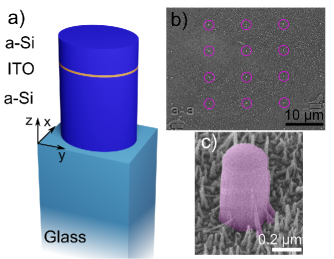
A schematic of the fabricated PGA is depicted in Figure 1 a). It consists of a high refractive index pillar of elliptical horizontal cross section in which a thin layer of ENZ material is embedded. The design stems from considerations discussed in a previous publication 17. The ENZ layer is placed at three quarters of the pillar’s height to improve the directivity of the antenna through modal interference. The pillar’s elliptical cross section is chosen to improve the antenna’s field enhancement by concentrating the light intensity midway through the pillar’s major radius. For operation in the near infrared, amorphous silicon (a-Si) and ITO are chosen as the high refractive index and ENZ materials respectively. Indium tin oxide, which is a conductive oxide commonly used as a transparent conductor, has an ENZ frequency in the near infrared. The exact crossing point of the real part of the permittivity, which is a consequence of the plasma frequency, and thus the carrier concentration, can be strongly tuned through the oxygen vacancy density21. In our highly conductive samples, the ITO ENZ wavelength was measured to be 1188 nm using variable angle spectroscopic ellipsometry (see Supplementary Figure S1) performed on a 30 nm-thick film grown under the same conditions as those used in our PGA.
The fabricated elliptical a-Si/ITO/a-Si PGAs have layer thicknesses of 373 nm, 10 nm and 128 nm, respectively. While the predicted field enhancement could be further increased for even thinner ITO films, 10 nm was chosen as it allows for relatively uniform films to be achieved directly using reactive sputtering under a wide range of conditions (see Supplementary Information Figure S2). Achieving high quality thinner (down to monolayer) films is possible, but requires substantial optimization of the deposition conditions or specialized printing techniques.22, 20 Antennas were patterned laterally using electron beam lithography (see Methods). Each fabricated array holds nominally identical pillars spaced 10 m apart to avoid coupling between pillars. To investigate the impact of the antenna dimensions on the response, three arrays (I, II and III) hosting antennas with different cross-sectional dimensions were investigated. Scanning electron microscope (SEM) micrographs of one of these arrays as well as a close up on a single antenna are shown in Figures 1 b) and c) respectively. The cross-sectional dimensions of the antennas in these arrays are summarized in Table 1. These were measured using top-down SEM micrographs shown in Figure S3 of supplementary information. These micrographs confirm that the fabricated structures are faithful to the design, but with some minor imperfections such as a slightly narrower top and the presence of micrograss between the antennas. The latter occurs to due to the random formation of silicon oxyfluoride micromasks during the etching of the bottom a-Si layer.23 However, as we will demonstrate with further optical characterisation, these have no measurable impact on the antenna response.
| Array index | Minor diameter (nm) | Major diameter (nm) |
|---|---|---|
| I | ||
| II | ||
| III |
To probe the linear optical response of the antennas, we first measure the far-field scattering spectrum of individual antennas in arrays I, II and III using single particle dark field scattering (DFS) spectroscopy.
The DFS spectra for an antenna representative of those in arrays I, II and III are plotted in Figure 2 a), b) and c) respectively.
The DFS spectra from other antennas of the same array are qualitatively similar with slight variations in peak intensities and position due to structural inhomogeneities between nominally identical antennas (see additional DFS spectra in Figure S3 of supplementary information).
The micrograss surrounding the antennas do not lead to any observable dark field scattering in the spectral region probed by our experiment (see Figure S4 of supplementary information).
The broadband DFS response covers nearly an octave and redshifts as the lateral dimensions of the antennas are increased from array I to III.

In Figure 2, we also compare our experimental data with the simulated scattering cross-section integrated over the collection objective’s numerical aperture. The dimensions reported in Table 1 were used for these calculations. The result for arrays I, II and III are plotted as dashed lines alongside the experimental data in Figure 2 a), b) and c) respectively. The resonant structure observed in the DFS spectra is faithfully reproduced for all dimensions but with narrower, slightly shifted features. These discrepancies are most likely due to small deviations from the idealized geometry and increased damping for the 10 nm film as compared to the measured refractive index.
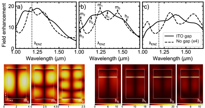
The agreement between the experimental DFS spectra and the simulated ones allows us to interpret the behavior of the antennas using the quasinormal modes of the simulated structures. The DFS spectra capture the far-field properties of the antennas. The near-field properties on the other hand, are better captured by the field enhancement spectra plotted in Figure 3. We define the field enhancement as the maximal ratio between the z-component of the electric field in the antenna to the magnitude of the incident electric field. The figure also shows the case of ungapped antennas to highlight the effect of the interaction between the ITO slab and the bare dielectric antenna modes. The antennas show very distinct resonances within the spectral region covered by the DFS bands. Like the DFS spectra, when the cross-sectionnal dimensions of the antennas are increased from Figure 3 a) to c), these resonances redshift and spread apart. Compared to the purely dielectric antennas, the ENZ PGA field enhancement spectra exhibit broader, shifted features, an additional resonance, and a fourfold increase in field enhancement. This behavior is a sign of the strong coupling between the dielectric antenna modes and the ITO plasmonic resonance at the ENZ wavelength. 18 While the interpretation is the same for all antenna dimensions, the modes are labelled and shown for the case of antenna II. Dielectric modes are identified by resonances in the ungapped antenna’s field enhancement spectra such as those labelled m0, m1 and m2 in Figure 3 b). A cross-section of the z-component of their internal electric field reveals horizontally anti-symmetric field distributions for all modes and an increasing number of vertical nodes with the mode index. The strength of the interaction between the bulk plasmon resonance and a given dielectric mode is related to the electric field’s z-component. By placing the ENZ layer at a quarter of the antenna’s height from the top, the ENZ mode couples most strongly to mode m1 then m0 and least to m2. This coupling creates new modes labelled h0, h1, h2 and h3 in Figure 3 b). These are shifted from the bare antenna modes by their interaction with the ENZ mode and broadened due to its increased damping. These hybrid light-matter modes inherit both the bare antenna modes’ coupling to the far-field and the strongly localized character of the ITO plasmonic resonance. These characteristics are clearly manifested in the antenna’s electric field profiles plotted in the mode-labelled panels of Figure 3 for the antennas of array II. All profiles taken within the field enhancement band show both a strong localization of the electric field within the ITO layer and a radiative component in and around the antenna. This ultimately manifests in the broadband field enhancements of 10-20 shown in Figure 3 as well as the efficient coupling to far-field radiation. The same interpretation holds for antennas I and III. It must be noted however, that some modes do not couple strongly to the ENZ layer. This is the case for mode h3 of antenna II, for example. Here, the ITO slab is located close to the node of the photonic mode m2, leading to a weak coupling with the ENZ mode.
We next probe the field enhancement occurring within the fabricated devices through THG. As any non-linear optical phenomenon, THG is a highly sensitive probe of the local field intensity created by a pump beam. As such, it has been widely used to probe field enhancements in metallic24 and dielectric25 optical nanoantennas, thin films of ENZ materials26, 10 and metasurfaces27. Our experimental setup allows us to image emission from the sample at the pump’s third harmonic and resolve the contribution of individual pillars (see Methods section for more details). The image of pillar array II illuminated by a 1.3 m pump, taken at the THG frequency, is shown in Figure 4 a). Intense emission is clearly visible at the antenna positions. No signal above the background is observed between the antennas, confirming the large field enhancement and the negligible role played by the grass-like background. To confirm that this emission stems indeed from THG, we check that it follows a cubic dependence on pump fluence. We compensate for variation in the pump profile over an array by acquiring an image of the pump spot at the sample such as the one shown in Figure 4 b) (see Methods for details). The power emitted from two antennas (A and B in Figure 4) are plotted against pump fluence in Figure 4 c). Both datasets are well fitted over three ordes of magnitude by a cubic dependance on pump fluence, confirming that the observed emission stems from THG inside the antenna. We cannot discard, however, the contribution of cascaded sum frequency processes to this emission28. Nevertheless, cascaded or not, THG remains a sensitive probe of field enhancement inside the antennas.
Despite being nominally identical, pillar B is about twice as brigh as pillar A. This reflects the presence of important structural differences between the antennas to which neither SEM nor DFS spectroscopy are sensitive to. This hints at the location of the THG process within the antennas. Great structural differences between antennas are unlikely to arise from the bulk of the silicon layers due to their amorphous structure, or from the antennas’ surfaces given their smooth profiles (see Figure S2b of supplementary information). On the other hand, the polycrystalline ITO layer is noticeably rough and features clear crystalline domains of tens of nanometers in size (see Figure S2a of supplementary information). When all but the antennas’ cross sections are etched away from the a-Si/ITO/a-Si multilayer, each antenna samples a different region of the inhomogeneous ITO layer. Since the antenna’s radiative properties depend on the overall mode profile, the DFS spectra are only weakly affected by variations in the microstructure. However, THG is highly sensitive to the permittivity at the mode hotspot. Since the hotspot is concentrated in the ITO, as shown in the panels of Figure 3, the microstructure variations are likely to cause the THG intensity variation between antennas.

We now check the contributions of the different antenna modes to THG. We can extract the antenna’s TH power conversion efficiency by dividing the time averaged emitted TH irradiance by the time-averaged received pump irradiance . Given that this number depends on and the pump pulse duration, a more meaningful result is obtained by instead defining the THG efficiency as the ratio of the peak TH irradiance to the cube of the peak pump irradiance. The observed cubic dependance on pump irradiance guarantees this metric to be independant of pump irradiance while using peak irradiance values accounts for the pump pulse duration. Lastly, the values reported here strongly underestimate the internal THG efficiency due to strong absorption of the TH within the a-Si dielectric and the finite numerical aperture of the collection objective. Simulations shown in Supplementary Information estimate that 98% of the generated TH power is absorbed by the a-Si and only 23% of the radiated TH is collected by our apparatus due to the highly anisotropic THG radiation profile.
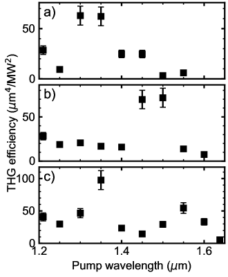
We measured the instantaneous THG efficiency of antennas within arrays I, II and III using pump wavelengths spanning 1.21 m to 1.64 m and plotted them in Figure 5 a) to c). The single antennas chosen for this investigation are the same as those whose DFS spectra are plotted in Figure 2. For all antennas, nm wide resonances are observed atop a broad THG response within the measured wavelengths. Just like in the DFS spectra, these resonances redshift with increasing lateral pillar dimensions. They also consistently match the experimental peaks observed in the DFS spectra of Figure 2. However, despite showing strong THG over their whole field enhancement band, the shape of the THG efficiency curves differ from the calculated field enhancement spectra cubed. Notably, the highest enhancement is observed for the widest antenna, in contrast to the prediction of Fig. 3. Several mechanisms can contribute to these differences. In particular, the a-Si’s absorption nearly triples over the probed TH spectral window of 550 nm to 400 nm29, which significantly reduces the radiated THG power at shorter wavelengths. In addition, the longitudinal and transverse components of ITO’s frequency dependent nonlinear susceptibility have been reported to increase by approximately and , respectively, in the range between 1020 nm to 1320 nm30. Finally, nonlocal effects, which have been ignored, and material roughness can play an important role in the generation and coupling of localized THG to far field radiation. While all antennas show strong THG over the spectral region probed, the amplitude of the resonances vary significantly between pillars within the same array (see supplementary material). This reflects the important local inhomogeneities between nominally similar antennas previously highlighted. For comparison’s sake, TH power conversion efficiencies measured for the antennas studied in Figure 5 are 8.6 at 3.7 GW/cm2, 4.7 at 2.6 GW/cm2 and 5.1 at 3.2 GW/cm2 for arrays I, II and III excited at 1.35, 1.45 and 1.55 m respectively. These figures include the large absorption losses in the a-Si and the limited collection efficiency. From simulations of the THG external coupling efficiency, we expect internal efficiencies to be 200 times larger than the figures reported here. Given that the dominant loss mechanism is simply re-absorption of the THG radiation within the a-Si, moving to a longer wavelengths or a transparent dielectric could alleviate these losses.
3 Conclusion
We have demonstrated photonic gap antennas in which an ultra thin layer of ITO, an ENZ material, is embedded. By comparing dark field scattering spectroscopy measurements with simulations of the antennas’ scattering cross-section, we showed the antennas host hybrid polaritonic modes in accordance with simulations and previous work. Through third harmonic generation, we confirm that these modes tightly confine the fields inside the 10 nm thick ITO layer, leading to high field enhancement over a broad spectral range of 400 nm. This proof of concept demonstrates the effectiveness of PGAs as vertically stacked optical antennas. They afford a strong localized field enhancement in an device that can be fabricated using photolithography or straightforward electron-beam lithography, forgoing the high lateral resolution requirements of traditional antenna designs. While our demonstration is in the near-infrared, PGAs are particularly attractive for applications in the mid-infrared where the ENZ frequency of doped III-V semiconductors is located31 . Using molecular beam epitaxy, infrared ENZ materials could be grown inside PGAs with deep subwavelength thicknesses well below those reported here and provide more than an order of magnitude larger field enhancement.
4 Acknowledgements
This work was supported by the Natural Sciences and Engineering Council of Canada Strategic Grant Program, the Canada Research Chairs Program and the Discovery Grants Program. We would also like to acknowledge design and fabrication support from CMC Microsystems and Canada’s National Design Network (CNDN).
4.1 Author Contributions
* F.T, D.M.M and A.P have contributed equally to this work.
5 Methods
5.1 Sample fabrication
A B270 glass substrate (51 mm x 51 mm and 2 mm thick) was pre-cleaned using an oxygen and argon plasma. The PGAs were fabricated by sputtering in a CMS-18 deposition system by Kurt J. Lesker using 3-inch targets of Si and ITO (In2O3/SnO2 90/10 wt %). Each layer of material was grown on a glass substrate to the desired thicknesses. A 372 nm layer of amorphous silicon was then sputtered at 200 °C, followed by a 10 nm layer of ITO sputtered at room temperature. The sample was then removed from the chamber and measured on a J.A. Woollam RC2-XI ellipsometer. After returning it to the sputtering chamber, it was annealed under vacuum for an hour at a 400 °C setpoint in order to reduce the epsilon-near-zero wavelength to 1188 nm. The temperature was then brought down to 200 °C for the sputtering of the final 128 nm layer of amorphous silicon. The layer thicknesses and bulk optical properties were measured using the same ellipsometer (see Figure S1 of supplementary information).
The large sample was cleaved into several smaller samples roughly equal in size, which were cleaned by sonication in acetone and isopropyl alcohol followed by ten minutes in an oxygen plasma (200 W, 0.8 mbar). Immediately before spin coating, each sample was vacuum baked (50 torr, 120 °C, five minutes) and primed with SurPass 3000. They were spin-coated with MA-N 2403 (4000 rpm) negative electron beam resist, pre-baked on a hotplate (90 °C, 1 minute), and exposed in a Raith 150 electron beam lithography system (20 kV, 80 C/cm2). Development was done in MA-D 525 developer (40 seconds) followed by two rinses in deionized water while stirring (10 minutes total) then by a post-bake on a hotplate (90 °C, 2 minutes). The samples were then mounted onto an \chAl2O3-coated silicon carrier wafer using Crystalbond and etched in an Oxford Instruments Plasmalab 100 ICP 180 reactive ion etching tool. The recipe for etching the top amorphous silicon (1200 W ICP power, 60 W RF, 49 V bias, 20 mtorr, 15 °C, 22 sccm \chSF6, 38 sccm \chC4F8, 16 seconds) is a pseudo-Bosch process similar to those used elsewhere for anisotropic etching of silicon 32, 33, 34, 35, 36. The sample was removed from the chamber and wet etched in an acid solution (1:3:4 \chHNO3/HCl/\chH2O) for 2 minutes to remove the ITO layer. The sample was reinserted in the chamber and etched a second time using the same peusdo-Bosch recipe for 35 more seconds, and finally cleaned in an oxygen plasma (2000 W ICP, 0 W RF, 35 mtorr, 15 °C, 30 seconds).
5.2 Optical characterisation
The optical characterisation setup used was designed to investigate both dark field scattering (DFS) and third harmonic generation (THG) in single antennas. This allows the direct correlation of individual DFS and THG spectra despite possible inhomogeneities between pillar specimens. A detailed diagram of this setup is presented in the supplementary information. The sample was held in an inverted microscope customized to allow illumination straight from the top through a 10x microscope objective for THG or at a grazing angle through a 10 mm biconvex lens for DFS spectroscopy. A stabilized laser lamp provided a broad and stable infrared illumination for the DFS experiments. The output of an optical parametric amplifier (200 fs pulse duration, 100 kHz repetition rate, Light Conversion ORPHEUS-N) was used to pump the THG. For both experiments, light was collected from the bottom of the microscope through a 40x 0.75 NA objective and sent to an infared spectral imager for DFS scattering spectroscopy or a visible light imaging system for THG. The collected light was directed to either systems using an accurate magnetically registered kinematic mount. The visible imager consists of a single lens, a visible shortpass filter (400 nm to 550 nm bandpass, Thorlabs FESH550) and a silicon CCD camera (Princeton Instruments Pixis 400) sensitive from 350 nm to 1000 nm. The infrared imager is composed of a InGaAs CCD camera (First Light C-RED2) sensitive from 800 nm to 1650 nm connected at the exit of an imaging spectrometer.
When performing DFS experiments, only the infrared imager was used with the spectrometer’s first diffractive order. The spectrum of the broadband light source was obtained by focusing it at the sample plane from within the collection objective’s numerical aperture and recording it using the infared imager. The spectrum of the DFS cross-section was obtained by dividing the scattered spectrum by that of the light source after proper background subtraction.
During THG measurements, the pump profile at the sample was first imaged using the infrared imager with its spectrometer at the zeroth order and a neutral density filter. The pump was then turned off with a mechanical shutter and the sample’s region of interest was moved under the pump’s illumination. The collection path is then reconfigured for the use of the visible imager and the pump shutter opened to acquire an image of the pump induced THG. Using a ruled sample, the infrared and visible imagers’ image planes are calibrated so that a location on one of these planes can be mapped onto the other. This allows for the measurement of the pump power density responsible for THG in a given pillar.
All pump powers were measured with a high resolution thermal power sensor (Thorlabs S401C). The third harmonic power was measured by calibrating the number of counts on the visible imager’s camera to the power emitted at the sample’s plane. This calibration was performed for every wavelength of interest using the same acquisition parameters as those used in the THG measurements.
References
- Edwards et al. 2008 Edwards, B.; Alù, A.; Young, M. E.; Silveirinha, M.; Engheta, N. Experimental Verification of Epsilon-Near-Zero Metamaterial Coupling and Energy Squeezing Using a Microwave Waveguide. Physical Review Letters 2008, 100, 033903
- Lobet et al. 2020 Lobet, M.; Liberal, I.; Knall, E. N.; Alam, M. Z.; Reshef, O.; Boyd, R. W.; Engheta, N.; Mazur, E. Fundamental Radiative Processes in Near-Zero-Index Media of Various Dimensionalities. ACS Photonics 2020, 7, 1965–1970
- Passler et al. 2019 Passler, N. C.; Razdolski, I.; Katzer, D. S.; Storm, D. F.; Caldwell, J. D.; Wolf, M.; Paarmann, A. Second Harmonic Generation from Phononic Epsilon-Near-Zero Berreman Modes in Ultrathin Polar Crystal Films. ACS Photonics 2019, 6, 1365–1371
- Reshef et al. 2019 Reshef, O.; De Leon, I.; Alam, M. Z.; Boyd, R. W. Nonlinear optical effects in epsilon-near-zero media. Nature Reviews Materials 2019, 4, 535–551
- Wen et al. 2018 Wen, X.; Li, G.; Gu, C.; Zhao, J.; Wang, S.; Jiang, C.; Palomba, S.; Martijn de Sterke, C.; Xiong, Q. Doubly Enhanced Second Harmonic Generation through Structural and Epsilon-near-Zero Resonances in TiN Nanostructures. ACS Photonics 2018, 5, 2087–2093
- Vassant et al. 2012 Vassant, S.; Hugonin, J.-P.; Marquier, F.; Greffet, J.-J. Berreman mode and epsilon near zero mode. Optics Express 2012, 20, 23971
- Campione et al. 2015 Campione, S.; Brener, I.; Marquier, F. Theory of epsilon-near-zero modes in ultrathin films. Physical Review B 2015, 91, 121408
- Alam et al. 2018 Alam, M. Z.; Schulz, S. A.; Upham, J.; De Leon, I.; Boyd, R. W. Large optical nonlinearity of nanoantennas coupled to an epsilon-near-zero material. Nature Photonics 2018, 12, 79–83
- Campione et al. 2015 Campione, S.; Liu, S.; Benz, A.; Klem, J. F.; Sinclair, M. B.; Brener, I. Epsilon-Near-Zero Modes for Tailored Light-Matter Interaction. Physical Review Applied 2015, 4, 044011
- Luk et al. 2015 Luk, T. S.; de Ceglia, D.; Liu, S.; Keeler, G. A.; Prasankumar, R. P.; Vincenti, M. A.; Scalora, M.; Sinclair, M. B.; Campione, S. Enhanced third harmonic generation from the epsilon-near-zero modes of ultrathin films. Applied Physics Letters 2015, 106, 151103
- Hendrickson et al. 2018 Hendrickson, J. R.; Vangala, S.; Dass, C.; Gibson, R.; Goldsmith, J.; Leedy, K.; Walker, D. E.; Cleary, J. W.; Kim, W.; Guo, J. Coupling of Epsilon-Near-Zero Mode to Gap Plasmon Mode for Flat-Top Wideband Perfect Light Absorption. ACS Photonics 2018, 5, 776–781
- Kim et al. 2016 Kim, J.; Dutta, A.; Naik, G. V.; Giles, A. J.; Bezares, F. J.; Ellis, C. T.; Tischler, J. G.; Mahmoud, A. M.; Caglayan, H.; Glembocki, O. J.; Kildishev, A. V.; Caldwell, J. D.; Boltasseva, A.; Engheta, N. Role of epsilon-near-zero substrates in the optical response of plasmonic antennas. Optica 2016, 3, 339
- Schulz et al. 2016 Schulz, S. A.; Tahir, A. A.; Alam, M. Z.; Upham, J.; De Leon, I.; Boyd, R. W. Optical response of dipole antennas on an epsilon-near-zero substrate. Physical Review A 2016, 93, 063846
- Campione et al. 2016 Campione, S.; Wendt, J. R.; Keeler, G. A.; Luk, T. S. Near-Infrared Strong Coupling between Metamaterials and Epsilon-near-Zero Modes in Degenerately Doped Semiconductor Nanolayers. ACS Photonics 2016, 3, 293–297
- Jun et al. 2013 Jun, Y. C.; Reno, J.; Ribaudo, T.; Shaner, E.; Greffet, J.-J.; Vassant, S.; Marquier, F.; Sinclair, M.; Brener, I. Epsilon-Near-Zero Strong Coupling in Metamaterial-Semiconductor Hybrid Structures. Nano Letters 2013, 13, 5391–5396
- Wang et al. 2022 Wang, K.; Liu, A.-Y.; Hsiao, H.-H.; Genet, C.; Ebbesen, T. Large Optical Nonlinearity of Dielectric Nanocavity-Assisted Mie Resonances Strongly Coupled to an Epsilon-near-Zero Mode. Nano Letters 2022, acs.nanolett.1c03876
- Patri et al. 2021 Patri, A.; Cognée, K. G.; Haeberlé, L.; Menon, V.; Caloz, C.; Kéna-Cohen, S. Photonic Gap Antennas Based on High-Index-Contrast Slot Waveguides. Physical Review Applied 2021, 16, 044065
- Patri et al. 2022 Patri, A.; Cognée, K. G.; Myers, D. M.; Haeberlé, L.; Menon, V.; Kéna-Cohen, S. Hybrid epsilon-near-zero modes of photonic gap antennas. Physical Review B 2022, 105, 165126
- Grinblat et al. 2017 Grinblat, G.; Li, Y.; Nielsen, M. P.; Oulton, R. F.; Maier, S. A. Degenerate Four-Wave Mixing in a Multiresonant Germanium Nanodisk. ACS Photonics 2017, 4, 2144–2149
- Datta et al. 2020 Datta, R. S. et al. Flexible two-dimensional indium tin oxide fabricated using a liquid metal printing technique. Nature Electronics 2020, 3, 51–58
- Cleary et al. 2018 Cleary, J. W.; Smith, E. M.; Leedy, K. D.; Grzybowski, G.; Guo, J. Optical and electrical properties of ultra-thin indium tin oxide nanofilms on silicon for infrared photonics. Optical Materials Express 2018, 8, 1231
- Li et al. 2019 Li, S.; Tian, M.; Gao, Q.; Wang, M.; Li, T.; Hu, Q.; Li, X.; Wu, Y. Nanometre-thin indium tin oxide for advanced high-performance electronics. Nature Materials 2019, 18, 1091–1097
- Jansen et al. 1995 Jansen, H.; Boer, M. d.; Legtenberg, R.; Elwenspoek, M. The black silicon method: a universal method for determining the parameter setting of a fluorine-based reactive ion etcher in deep silicon trench etching with profile control. Journal of Micromechanics and Microengineering 1995, 5, 115–120
- Hanke et al. 2009 Hanke, T.; Krauss, G.; Träutlein, D.; Wild, B.; Bratschitsch, R.; Leitenstorfer, A. Efficient Nonlinear Light Emission of Single Gold Optical Antennas Driven by Few-Cycle Near-Infrared Pulses. Physical Review Letters 2009, 103, 257404
- Xu et al. 2018 Xu, L.; Rahmani, M.; Zangeneh Kamali, K.; Lamprianidis, A.; Ghirardini, L.; Sautter, J.; Camacho-Morales, R.; Chen, H.; Parry, M.; Staude, I.; Zhang, G.; Neshev, D.; Miroshnichenko, A. E. Boosting third-harmonic generation by a mirror-enhanced anapole resonator. Light: Science & Applications 2018, 7, 44
- Capretti et al. 2015 Capretti, A.; Wang, Y.; Engheta, N.; Dal Negro, L. Enhanced third-harmonic generation in Si-compatible epsilon-near-zero indium tin oxide nanolayers. Optics Letters 2015, 40, 1500
- Tong et al. 2016 Tong, W.; Gong, C.; Liu, X.; Yuan, S.; Huang, Q.; Xia, J.; Wang, Y. Enhanced third harmonic generation in a silicon metasurface using trapped mode. Optics Express 2016, 24, 19661
- Celebrano et al. 2019 Celebrano, M.; Locatelli, A.; Ghirardini, L.; Pellegrini, G.; Biagioni, P.; Zilli, A.; Wu, X.; Grossmann, S.; Carletti, L.; De Angelis, C.; Duò, L.; Hecht, B.; Finazzi, M. Evidence of Cascaded Third-Harmonic Generation in Noncentrosymmetric Gold Nanoantennas. Nano Letters 2019, 19, 7013–7020
- Pierce and Spicer 1972 Pierce, D. T.; Spicer, W. E. Electronic Structure of Amorphous Si from Photoemission and Optical Studies. Physical Review B 1972, 5, 3017–3029
- Rodríguez-Suné et al. 2021 Rodríguez-Suné, L.; Trull, J.; Akozbek, N.; de Ceglia, D.; Vincenti, M. A.; Scalora, M.; Cojocaru, C. Retrieving Linear and Nonlinear Optical Dispersions of Matter: Combined Experiment-Numerical Ellipsometry in Silicon, Gold and Indium Tin Oxide. Frontiers in Photonics 2021, 2, 746341
- Jun et al. 2014 Jun, Y. C.; Luk, T. S.; Robert Ellis, A.; Klem, J. F.; Brener, I. Doping-tunable thermal emission from plasmon polaritons in semiconductor epsilon-near-zero thin films. Applied Physics Letters 2014, 105, 131109
- Con et al. 2014 Con, C.; Zhang, J.; Cui, B. Nanofabrication of high aspect ratio structures using an evaporated resist containing metal. Nanotechnology 2014, 25, 175301
- Saffih et al. 2014 Saffih, F.; Con, C.; Alshammari, A.; Yavuz, M.; Cui, B. Fabrication of silicon nanostructures with large taper angle by reactive ion etching. Journal of Vacuum Science & Technology B, Nanotechnology and Microelectronics: Materials, Processing, Measurement, and Phenomena 2014, 32, 06FI04
- Khorasaninejad et al. 2012 Khorasaninejad, M.; Walia, J.; Saini, S. S. Enhanced first-order Raman scattering from arrays of vertical silicon nanowires. Nanotechnology 2012, 23, 275706
- Ayari-Kanoun et al. 2016 Ayari-Kanoun, A.; Aydinoglu, F.; Cui, B.; Saffih, F. Silicon nanostructures with very large negatively tapered profile by inductively coupled plasma-RIE. Journal of Vacuum Science & Technology B, Nanotechnology and Microelectronics: Materials, Processing, Measurement, and Phenomena 2016, 34, 06KD01
- Henry et al. 2009 Henry, M. D.; Walavalkar, S.; Homyk, A.; Scherer, A. Alumina etch masks for fabrication of high-aspect-ratio silicon micropillars and nanopillars. Nanotechnology 2009, 20, 255305