Circuit simulation using explicit methods
Abstract
Use of explicit methods for simulating electrical circuits, especially for power electronics applications, is described. Application of the forward Euler method to a half-wave rectifier is discussed, and the limitations of a fixed-step method are pointed out. Implementation of the Runge-Kutta-Fehlberg (RKF) method, which allows variable time steps, for the half-wave rectifier circuit is discussed, and its advantages pointed out. Formulation of circuit equations for the purpose of simulation using the RKF method is described for some more examples. Stability and accuracy issues related to power electronic circuits are brought out, and mechanisms to address them are presented. Future plans related to this work are described.
1 Introduction
Circuit simulation packages (e.g., NGSPICE [1], PSIM [2], PSCAD [3]) generally employ implicit methods, such as backward Euler and trapezoidal, for discretising the circuit equations involving time derivatives. Since these implicit methods are unconditionally stable, the simulator time steps are not constrained by stability issues. In other words, with these methods, the time step size is determined by accuracy considerations rather than stability constraints [4]. Therefore, even though they involve more work per time step, implicit methods are still the only practical option for circuits with very small time constants.
On the other hand, explicit methods, such as the Runge-Kutta-Fehlberg (RKF) [5] and Dormand-Prince (DP) [6] 4-5 pairs, involve less work per time step, and are ideally suited for non-stiff systems in which the time constants are not too small. Unfortunately, many circuits of practical interest do involve small time constants arising from the small on-state resistance of a switch or a small capacitance associated with a semiconductor device. In such cases, a simulator using an explicit method is forced to take very small time steps although accuracy considerations would allow much larger time steps. Application of explicit methods to electronic circuits is therefore severely limited.
Power electronic circuits offer a unique opportunity to utilise the efficiency – due to smaller computational effort per time step – of explicit methods if the switches are treated as ideal. The simulator PLECS [7] exploits this idea to enable fast simulation of a variety of power electronic circuits. However, owing probably to the commercial nature of PLECS, hardly any details are available in the public domain about how the ideas broadly described in the PLECS 4.6 manual are actually implemented.
It is the purpose of this paper to discuss various issues related to the use of explicit methods for power electronic circuit simulation. We consider a few examples to illustrate the basic implementation scheme, the various challenges, and some ways to address them.
2 Half-wave rectifier
A half-wave rectifier circuit is shown in Fig. 1.

In the following, we discuss how this circuit can be handled using an implicit method (backward Euler), an explicit method with a fixed time step (forward Euler), and an explicit method with a variable time step (RKF). The parameter values considered in all cases are: = V, = Hz, = mF, =. The on-state voltage drop for the diode is taken to be = V.
2.1 Backward Euler (BE) method
The capacitor equation, = is discretised using the BE method as,
| (1) |
where , denote the numerically obtained value of at =, =, respectively. In the context of the half-wave rectifier circuit, Eq. 1 gives,
| (2) |
Using Eq. 2 and the Modified Nodal Analysis (MNA) approach [8] for assembling circuit equations, we get
| (3) |
| (4) |
| (5) |
where =. The diode has been modelled as =, where = if the diode is conducting, and = if it is not. By making and sufficiently small and large, respectively, ideal diode behaviour can be realised.
Note that Eqs. 3-5 form a nonlinear set of equations (in , , ) since is a nonlinear function of the diode voltage . To solve this system of equations, circuit simulators generally employ the Newton-Raphson (N-R) iterative method in which the Jacobian equation must be solved for a few N-R iterations at each time point, thus making the procedure computationally expensive.
On the positive side, the backward Euler method is unconditionally stable and therefore does not impose an upper limit on the time step from the stability perspective. Furthermore, it allows complicated semiconductor device models to be incorporated in a straightforward manner.
2.2 Forward Euler (FE) method
The capacitor equation for the circuit of Fig. 1 can be discretised using the FE method as,
| (6) |
Since , are already known, can be found simply by evaluation, i.e.,
| (7) |
We can now obtain the rest of the variables at by writing the circuit equations, treating as a known entity. The resulting equations can be written, for example, as
| (8) |
| (9) |
| (10) |
a system of three equations in three variables: , , . Note that is still a nonlinear function of , making the situation similar to the backward Euler case.
In the interest of reducing the computation effort per time step, we now replace the original circuit with two circuits, one with the diode on, the other with the diode off, as shown in Fig. 2.

Each of the two circuits is linear, with an associated set of equations (Eqs. 8-10), with = in one case, and = in the other. Eqs. 8-10 can be written in the form =. For example, with the diode on, we have
| (11) |
where =. Note that the time step is not involved in the equations, and therefore the matrices are independent of time. This has a major implication, viz., and for a specific switch configuration needs to be computed only once, offering a very significant speed-up with respect to an implicit method.
In some circuits, replacing a switch with or can create stability issues because , a small resistance, can result in small -type time constants, and , a large resistance, in small -type time constants. In such cases, the simulator would be forced to take very small time steps. It is therefore preferable to make = and =, i.e., replace the switch with a short or open circuit.
In the half-wave rectifier circuit, using = creates a problem: The voltage source comes directly across the capacitor, and the matrix becomes singular. A slight modification of the circuit, viz., addition of a resistance in series with the capacitor, as shown in Fig. 3, circumvents this problem. The resistance should be small (taken as 10 m in this paper) so that it does not change the circuit operation.

There are different ways in which the set of equations for the on and off circuits of Fig. 3 can be written. In the following, we opt for a systematic procedure which can be easily extended to other circuits. We write the KCL equations at all nodes except the reference node, followed by the element equations. Note that
| (12) |
is treated as a known value. The set of equations is then given by
| (13) |
| (14) |
| (15) |
| (16) |
| (17) |
| (18) |
| (19) |
| (20) |
Eqs. 13-20 can be described in a matrix form, =, where the solution vector x consists of , , , , , , , , and b includes and , both being known values. Since the circuit has one switch, we have two possible A matrices, and , corresponding to the diode in the on and off state, respectively. In general, the number of A matrices would be , where is the number of switches in the circuit. After solving =, we need to make sure that the diode state is consistent with the A matrix which was used in the computation. For example, in the half-wave rectifier case, if was used, then must turn out to be positive. If it is not, we need to reject the solution, use instead, and solve = again. If has already been computed (and stored) earlier, solving = takes a small computational effort.
Note that it is not necessary to pre-compute the A and matrices for all switch configurations. In may power electronic circuits, only a small fraction of the switch configurations get actually visited, and pre-computing (and storing) all possible A and matrices would be wasteful in terms of time and memory. Instead, the matrices should be computed and stored dynamically, i.e., whenever a specific switch configuration is encountered. The overall procedure can be summarised as shown in Algorithm 1. We will refer to this scheme of using an explicit method for electrical circuits as the ELEX (ELectrical EXplicit) scheme. For reasons explained in the following, the FE method is not a good candidate for the ELEX scheme. Instead, a variable time-step method (for example, RKF or DP) would be preferred.
We now comment on stability issues related to the FE method when applied to the circuit of Fig. 3. The charging and discharging time constants, and , are given by
| (21) |
| (22) |
The FE method becomes unstable when the time step is larger than . Clearly, we need to use smaller than or 20 sec in the charging phase. Since the FE method is a fixed time step method, we end up using this small time step (20 sec) throughout the simulation, requiring at least = or time points in one period. From the accuracy point, such a large number of time steps is not required, and the FE method is therefore too slow for many applications.
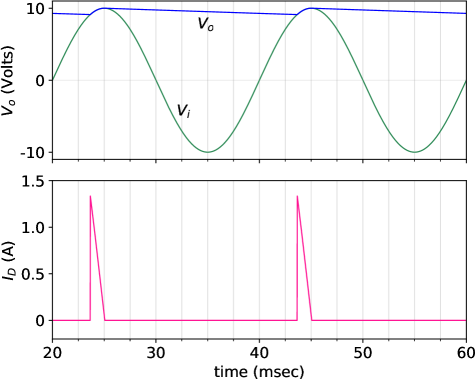
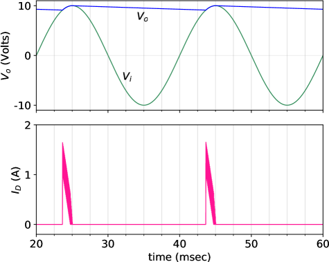
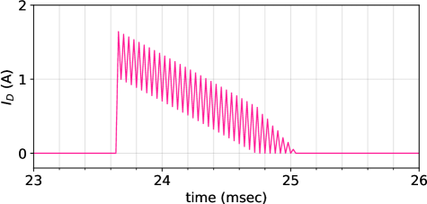
The stability problem is illustrated in Figs. 4 and 5. When sec is used (Fig. 4), the simulation results are as expected. For =sec (Figs. 5 and 6), oscillations can be seen in the diode current, indicating unstable behaviour of the FE method.
2.3 Runge-Kutta-Fehlberg (RKF) method
The RKF method is an adaptive (variable) time step method in which a Runge-Kutta method of order four is used together with a Runge-Kutta method of order five to obtain an estimate of the local truncation error (LTE) in a given time step. If the LTE is smaller than a user-specified tolerance, the next time step is allowed to be larger than the current time step. On the other hand, if the LTE is larger than the tolerance, then the current time step is rejected, and a smaller time step is tried. The RKF method requires more work at each time step (six function evaluations) as compared to the FE method (one function evaluation). However, its auto time step feature allows a dramatic reduction in the total number of time points required for the simulation while simultaneously satisfying the LTE constraint, and it is therefore much more efficient than the FE method.
The RKF method for a single ordinary differential equation (ODE) = can be described as follows. First, compute , , , as,
| (23) | |||||
| (24) | |||||
| (25) | |||||
| (26) | |||||
| (27) | |||||
| (28) |
where . The fourth- and fifth-order estimates for are then given by
| (29) | |||||
| (30) |
The constants , , in the above equations can be found in [5]. The difference between the fourth- and fifth-order values gives an estimate of the LTE. If the LTE is smaller than a tolerance, then the fifth order value is accepted as the numerical solution of the ODE at ; if not, the current time step is rejected, and a revised value of is computed, using the LTE estimate [5].
For the half-wave rectifier of Fig. 3, the ODE comes from the capacitor and is given by
| (31) |
(see Fig. 3). The first step in applying the RKF method to this problem is to compute (see Eq. 23) as
| (32) |
where is the numerical solution for at and is already known. For the next RKF step (Eq. 24), we compute an intermediate value of (denoted by ) using the following steps.
-
(i)
Update as
(33) -
(ii)
Update as
(34) -
(iii)
Solve the following set of equations, making sure that the A matrix (corresponding to diode on or off) used for solving the equations is consistent with the solution.
(35) (36) (37) (38) (39) (40) (41) (42)
We are now in a position to compute and as
| (43) |
| (44) |
We then compute as , solve the circuit equations to obtain , and compute . Proceeding in this manner, we compute , , , , and finally the fourth- and fifth-order estimates for (Eqs. 29 and 30). If there are several capacitors and inductors in the circuit, we would evaluate Eq. 33 for each of the state variables (inductor currents and capacitor voltages), update source value(s), and then solve the electrical equations.
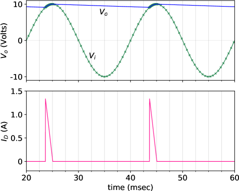
Fig. 7 shows the results obtained with the RKF method. The time points used by the RKF method are shown by crosses in the plot. It can be seen that, in the charging phase (where the time constant is small), small time steps are taken by the RKF method. In the discharging phase, the time constant is large, and much larger time steps – limited in this case by a user-specified maximum time step of 0.5 msec – are taken by the RKF method, thus leading to a much smaller number of total time points, as compared to the FE method.
The half-wave rectifier example brings out the fundamental limitation of using explicit methods for electrical circuits, viz., the necessity of using small time steps because of stability constraints. However, in several power electronic circuits of interest, the ELEX scheme essentially bypasses the stability issue by avoiding small time constants altogether, and in that case, the time step is limited by accuracy, rather than stability.
3 Switches in series
Consider the controlled switch, e.g., an idealised MOS transistor, shown in Fig. 8 (a).

In the ELEX scheme, we can write the switch equation as
| (45) |
In most situations, the above approach would work fine. However, this simple model can fail for some specific situations. As an example, consider the circuit shown in Fig. 8 (b) in which is a dc (known) voltage. If = and =, we expect =. If = and =, we expect = (see Fig. 9). When both and are zero, we would expect the applied voltage to split equally between the two switches, and should therefore be 5 V, as shown in Fig. 9. Let us now apply the ELEX scheme to this circuit.
Once again, we write the equations in a systematic manner, writing the KCL equations first, followed by the element equations, and get
| (46) |
| (47) |
| (48) |
| (49) |
| (50) |
where we have applied Eq. 45 to each of the two switches.
If one of and is high, Eqs. 46-50 give us the expected result. For the case ==, no solution is possible because node becomes isolated. In other words, if the equations are written in the form =, then A turns out to be singular. Although this situation is rare in power electronic circuits, a general-purpose simulation program must be able to handle it suitably.
When both and are off, we expect to divide equally between them, which suggests that the switch should be modelled as a large resistance in the off state. However, in the ELEX scheme, we would like to avoid such a representation because of its potential to create small -type time constants. What we need is a procedure that allows voltage division between the switches, but without replacing the switch with . One way to achieve these conflicting goals is as follows.
When the gate voltage is high, we continue to model the switch with the ideal switch equation
| (51) |
When the gate voltage is low, we use the model shown in Fig. 10, where = is a small conductance.

The current is given by,
| (52) |
where takes values, 1, 2, , . The switch current in the off state is then given by
| (53) |
With =, Eq. 53 amounts to removing the current source in Fig. 10, keeping only . When the circuit equations are solved for this condition, voltages get suitably assigned. For the example of Fig. 8 (b), we would get =. When =, Eq. 53 reduces to =, the ideal switch equation in the off state, since and become equal. Thus, by increasing from 1 to , we achieve our objective of establishing appropriate node voltages without replacing the switch with . For the circuit of of Fig. 8 (b), = is adequate. It remains to be seen if a larger value of is necessary for some other circuits.
Eq. 53, for a given value of , is solved in an iterative manner, treating , on the right-hand side (RHS) as known values coming from the previously computed solution. The RHS becomes part of b in =, the complete set of circuit equations. Solving =, we obtain revised values of , , and use those to compute the RHS of Eq. 53 again, and so on until convergence. For the circuit of Fig. 8 (b), two iterations suffice.
Clearly, the above procedure comes with an additional computational cost and should therefore be used only if the ideal switch model (Eq. 45) is creating a singular matrix situation. In most power electronic circuits, the ideal switch model seems to work well.
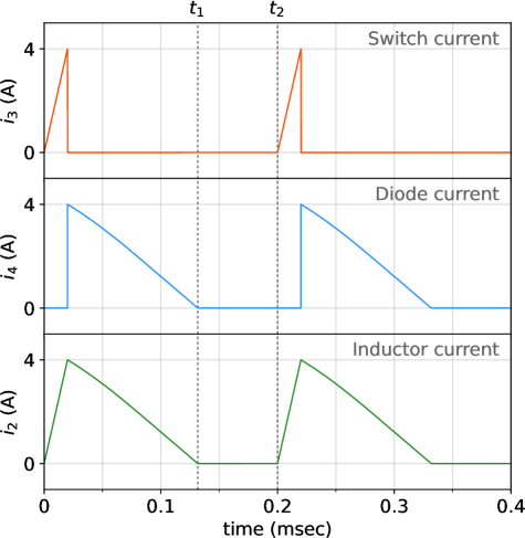
4 Boost converter
Consider the boost converter circuit shown in Fig. 11. For the parameter values given in the figure, the inductor current (in the steady state) is discontinuous, as shown in Fig. 12. The purpose of this section is to describe the challenges presented by the discontinuous nature of the inductor current and to present a way to address the same.

The ELEX-RKF procedure to obtain the solution at – assuming as always the solution at to be already available – starts with
| (54) |
| (55) |
for the capacitor and inductor, respectively. The inductor voltage for this circuit is =.
Next, we obtain and , the phase-2 updates for and , as
| (56) |
| (57) |
update the gate voltage value for the MOS switch, and then solve the set of circuit equations given by
| (58) |
| (59) |
| (60) |
| (61) |
| (62) |
| (63) |
| (64) |
| (65) |
| (66) |
| (67) |
| (68) |
Having obtained the solution at stage 2 of the RKF process, we then proceed to compute , , solve the circuit equations to obtain the solution at stage 3, and so on. In a way, this is a straightforward extension of the ELEX-RKF scheme we have seen in Sec. 2.3. However, one major change is required.
In the interval from to in Fig. 12, both and are off, i.e., ==. With this condition, the = problem described by Eqs. 58-68 has no solution because A becomes singular. Intuitively, we would expect that to happen since we are trying to assign a value to the inductor current when there is no path for that current. Even a boost converter which has continuous conduction in the steady state can go through the above situation (where both and are simultaneously off) in the transient phase, i.e., before steady state is attained by the circuit.
The singular matrix issue can be addressed by connecting a resistance in parallel with as shown in Fig. 13.

The value should be chosen to be sufficiently large (say, 1 M) such that it draws a negligibly small current, thus leaving the circuit solution essentially undisturbed. With in place, the inductor current equation (Eq. 62) gets replaced by
| (69) |
and the circuit matrix A remains non-singular even if and in Fig. 11 become zero.
The turn-off process of the diode at time (see Fig. 12) needs to be carefully handled for the following reason. The inductor current in the ELEX-RKF scheme gets updated in several stages of the RKF process, the first step being
| (70) |
where and come from the solution obtained at =. It is crucial to catch the diode turn-off point as closely as possible, i.e., the diode current should be sufficiently small before we move on to the off condition of the diode. This is achieved in the ELEX scheme using binary search – as in the PLECS [7] program – where we keep narrowing the bracket around the exact turn-off point, until it becomes acceptably small, say, = sec. When that is achieved, we have two simulation time points, one before and one after the turn-off event, the interval between them being . Let us denote these two points by and . At , the diode is still on, but ( in Fig. 11) is small, say, A or smaller. At , the diode has turned off, is exactly zero, and KCL implies that (in Fig. 11) is also zero, since the MOS switch is already off. The currents and in Fig. 13 at = cancel each other exactly. These currents are individually small but not zero. Considering this situation, in order to ensure that goes to zero quickly, we can use
| (71) |
rather than Eq. 70. Note that has been replaced with on the right-hand side in Eq. 71.
With the above modification, the ELEX-RKF scheme was able to handle the boost converter circuit of Fig. 11 accurately. It was observed that, if the diode current at is not small enough, the inductor current does not reduce to zero. As we proceed to the off state of the diode, we have a situation in which both the diode and MOS switch are off, and = (Fig. 13). In other words, current circulates in the - loop. This is a disastrous situation because the small time constant of the - loop forces the RKF process to take very small time steps, and the simulation becomes impractically slow.
In a general scenario, the - combination is useful in another sense. If a substantial inductor current is forced to become zero abruptly, the current would then go through , causing an unrealistically large voltage drop across the inductor. This voltage drop can be monitored by the simulator to issue a suitable warning or error message.
5 Closed-loop circuits
In a closed-loop power electronic circuit, additional variables related to the control block are involved. Typically, the electrical circuit produces one or more feedback quantities (currents or voltages), which serve as inputs to the control block, as shown in Fig. 14.

The control block in turn generates the gate signals required by the electrical circuit. In general, the control block is easier to handle than the electrical block because it involves only a “flow graph” and not a network where KCL and KVL equations need to be satisfied. When an explicit method is used to handle the control block, as we would be doing in the ELEX-RKF scheme, several “passes” are made to treat the elements of the control block, as dictated by the flow graph (see [9], [10]). In each pass, only those elements whose input values have been updated are processed. In the following, we will consider two examples to illustrate how the ELEX-RKF scheme can be applied to closed-loop circuits.
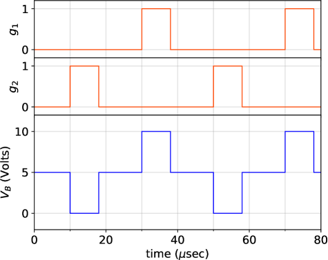
5.1 Current-controlled two-level voltage source converter
The circuit diagram for a current-controlled two-level voltage source converter is shown in Fig. 15, along with the control block.

We have already seen how voltage sources, MOS switches, resistors, inductors, are treated in the ELEX-RKF scheme. Let us see how the two new electrical elements in this circuit, viz., ammeter and voltmeter, can be handled. The ammeter is like a dc voltage source with = V, satisfying the equations,
| (72) |
| (73) |
The voltmeter is like a dc current source with = A, satisfying the equations,
| (74) |
| (75) |
The element equations, together with the KCL equations, constitute the set of electrical equations which, as we have seen in Sec. 4, can be written in the form =. Note that the feedback variables, and , are also included in x.
At each stage of the RKF process, we solve the electrical equations and obtain , . This is followed by updating the “control” variables , , , , , , and finally the gate signals to . In this example, the control block does not involve any state variables.
The control variables are updated as follows. First, we treat the source elements by assigning suitable values to and . The rest of the control variables are then updated as
| (76) |
| (77) |
| (78) |
| (79) |
The gate signals to are then obtained by comparing or with .
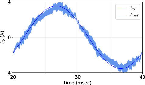
In the interest of resolving the gate signal waveforms accurately, the simulator time steps are limited by placing additional time points before and after the expected cross-over points of the comparators, as described in [11]. Simulation results obtained for are shown in Fig. 16, along with the reference current .
The two currents are shown on an expanded scale in Fig. 17.
Simulation results obtained for , when the comparator cross-over time points are not treated accurately (with all other simulation parameters the same), are shown in Fig. 18. By comparing Figs. 16 and 18, we can clearly see that simulation accuracy is significantly affected by correct treatment of comparator cross-over.
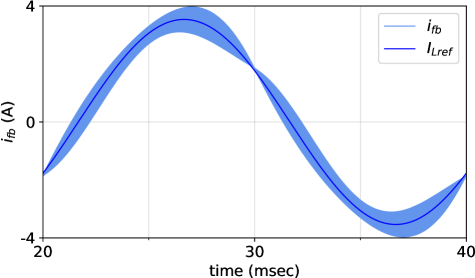
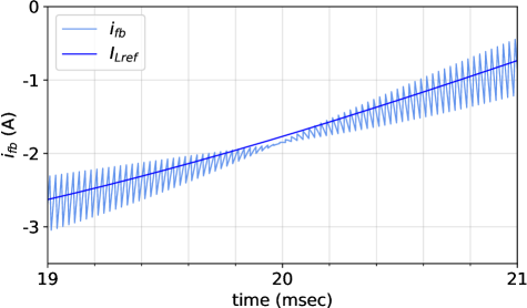
5.2 Voltage-controlled buck DC-DC converter
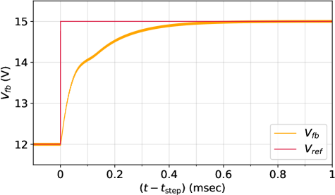
Fig. 19 shows a voltage-controlled buck DC-DC converter, with the voltage reference changing from 12 to 15 V at = msec.

The transfer function of the filter is given by
| (80) |
where =, = rad/s, and = rad/s. For simulation of the circuit using the ELEX-RKF scheme, we rewrite as
| (81) |
where =. The control block can now be implemented as shown in Fig. 20.

As in the previous example, at each stage of the RKF method, we solve the electrical equations (=), followed by updating the control block variables, and then proceed to the next RKF stage. The control block variables are treated by first upgrading the two integrator outputs. For example, in RKF stage 2, we would have
| (82) |
| (83) |
and limit as . Next, we update the and (sawtooth) source values at , and then compute the remaining control variables as,
| (84) |
| (85) |
| (86) |
| (87) |
| (88) |
| (89) |
| (90) |
| (91) |
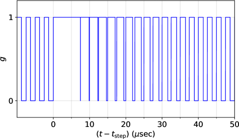
Fig. 21 shows and , and Fig. 22 shows the gate pulses produced by the controller when changes from 12 V to 15 V at =.
6 Conclusions and future work
In summary, we have presented a methodology called ELEX-RKF for using explicit methods – in particular the RKF method – for simulation of power electronic circuits, considering the switches to be ideal. The reasons for higher simulation speed of the ELEX-RKF scheme as compared to implicit schemes are explained. Several challenges which are encountered in implementing the ELEX-RKF scheme are pointed out. With the help of suitable examples, these issues are illustrated, and techniques are descried for resolving the same. Simulation results obtained using the ELEX-RKF scheme are presented for a few representative power electronic circuits.
The following future work is planned.
-
1.
The ELEX-RKF scheme will be implemented in the open-source simulation package GSEIM [12], [13]. At the time of writing, GSEIM allows only implicit methods for electrical circuits, together with MNA for circuit equation formulation. Incorporation of the ELEX-RKF option will make GSEIM more versatile, and particularly useful for circuits which take a substantial amount of time with implicit methods.
-
2.
PLECS [7] uses the Dormand-Prince (DP) 4-5 pair for solving the ODEs. Implementation of the DP method is conceptually very similar to the RKF method. It is envisaged that GSEIM will allow both ELEX-RKF and ELEX-DP options to the user.
-
3.
In this work, we have not compared simulation times of the ELEX-RKF scheme with implicit methods. In future, we plan to use GSEIM to make such a comparison for typical power electronic circuits, thus enabling the user to make an informed choice about the solution method.
References
- [1] P. Nenzi, “NGSPICE circuit simulator release 26, 2014.”
- [2] PSIM. [Online]. Available: https://powersimtech.com/products/psim/capabilities-applications/
- [3] PSCAD. [Online]. Available: https://www.pscad.com/
- [4] M.B. Patil, V. Ramanarayanan, V.T. Ranganathan, Simulation of power electronic circuits. New Delhi: Narosa, 2009.
- [5] R.L. Burden and J.D. Faires, Numerical Analysis. Singapore: Thomson, 2001.
- [6] Dormand-Prince method. [Online]. Available: https://en.wikipedia.org/wiki/Dormand%E2%80%93Prince_method
- [7] PLECS 4.6. [Online]. Available: https://www.plexim.com/products/plecs
- [8] W.J. McCalla, Fundamentals of Computer-Aided Circuit Simulation. Boston: Kluwer Academic Publishers, 1987.
- [9] M.B. Patil. SEQUEL Users’ Manual: Part-1. [Online]. Available: http://www.ee.iitb.ac.in/~sequel
- [10] GSEIM users manual. [Online]. Available: https://gseim.github.io/build/html/index.html
- [11] M. B. Patil, R. D. Korgaonkar, and K. Appaiah, “GSEIM: a general-purpose simulator with explicit and implicit methods,” Sādhanā, vol. 46, no. 4, pp. 1–13, 2021.
- [12] M.B. Patil, V.V.S. Pavan Kumar Hari, Ruchita D. Korgaonkar, and Kumar Appaiah, “An open-source simulation package for power electronics education,” available at https://arxiv.org/abs/2204.12924.
- [13] GSEIM. [Online]. Available: https://github.com/gseim/gseim