Bridging Borophene and Metal Surfaces:
Structural, Electronic, and Electron Transport Properties
Abstract
Currently, solid interfaces composed of two-dimensional materials (2D) in contact with metal surfaces (m-surf) have been the subject of intense research, where the borophene bilayer (BBL) has been considered a prominent material for the development of electronic devices based on 2D platforms. In this work, we present a theoretical study of the energetic, structural, and electronic properties of the BBL/m-surf interface, with m-surf = Ag, Au, and Al (111) surfaces, and the electronic transport properties of BBL channels connected to the BBL/m-surf top contacts. We find that the bottom-most BBL layer becomes metalized, due to the orbital hybridization with the metal surface states, resulting in BBL/m-surf ohmic contacts, meanwhile, the inner and top-most boron layers kept their semiconducting character. The net charge transfers reveal that BBL has become -type (-type) doped for m-surf = Ag, and Al (= Au). A thorough structural characterization of the BBL/m-surf interface, using a series of simulations of the X-ray photoelectron spectra, shows that the formation of BBL/m-surf interface is characterized by a redshift of the B- spectra. Further electronic transport results revealed the emergence of a Schottky barrier between 0.1 and 0.2 eV between the BBL/m-surf contact and the BBL channels. We believe that our findings are timely, bringing important contributions to the applicability of borophene bilayers for developing 2D electronic devices.
I Introduction
Two-dimensional (2D) materials have been intensively studied with a focus on both fundamental issues and practical applications addressing the development of novel electronic devices. Since the successful synthesis of graphene,1 other 2D systems have been found/proposed, such as single-layer (SL) transition metal dichalcogenides (TMDs), like MoS2 and WSe2 SLs,2; 3 and graphene counterparts like silicene,4 germanene,5 phosphorene.6
Because of its peculiar electronic structure, boron atoms can exist in a wide range of structural phases, including 2D sheets referred to as borophene.7; 8; 9; 10; 11; 12 In a seminal work, Mannix et al.11 synthesized single-layer borophene on the Ag(111) surface, characterized by a buckled structure of boron atoms forming a triangular lattice. In the sequence, Feng et al.12 synthesized a planar and more stable SL borophene structure distinguished by the formation of periodic holes embedded in a triangular lattice. Other metal surfaces, besides Ag(111), have also been utilized as a substrate for the borophene’s synthesis, for instance, Al(111), Au(111), Cu(111), and Ir(111).13; 14
Theoretical research on the electronic characteristics of borophene has been stimulated by the polymorphism of 2D systems based on boron atoms. For instance, (i) exotic electronic properties, like the formation of Dirac nodal lines15 and the formation of chiral states in borophene bilayer systems,16 among other electronic features. In parallel, (ii) combined with atomic-scale material engineering, borophene heterostructures have been successfully synthesized. For instance, lateral superlattices are composed of (periodic) rows of borophene single layer (BSL) with different structural phases.17 In a recent study, we predicted the emergence of electronic confinement effects and anisotropic electronic transport in those borophene lateral superlattices.18; 19
Further theoretical studies have predicted the formation of interlayer chemical bonds between SL borophene sheets, resulting in borophene bilayer (BBL) systems.20 Indeed, semiconductor BBLs were produced on metal surfaces like Ag(111) and Cu(111),21; 22; 23 and subsequent first-principles computations verified their energetic and structural stability.24
A solid understanding of the structural and electronic properties of new materials is fundamental for the development of electronic devices. Here, computational simulations, based on first-principles methods, have been viewed as a promising solution for a comprehensive atomic scale understanding of the electronic and structural properties of materials in general. For instance, in 2D systems like MoS2/metal,25; 26; 27; 28 phosphorene/metal,29; 30 and more recently BBL/metal interfaces.24; 31; 32
Currently, the applications of new materials in ”two-dimensional electronics” relies on critical issues like the understanding of the electronic and structural properties of metal/semiconductor interfaces and the emergence of electronic transport throughout 2D semiconductor channels. 33; 34; 35 In this work, we used first-principles calculations to investigate (i) the energetic, structural, and electronic properties of bilayer borophene (BBL) on different metal surfaces (m-surf), specifically Ag(111), Au(111), and Al(111), denoted as BBL/m-surf, and (ii) the electronic transport properties through BBL channels (ch) under different BBL/m-surf top contacts (tc), which we describe as [BBL/m-surf] - [BBL] - [BBL/m-surf]. In (i), we focus on the interfacial hybridizations that govern the formation of BBL/m-surf, resulting in either - or -type doping of the BBL, the formation of an ohmic contact at the semiconductor/metal interface, and the m-surf BBL tunneling barrier. In (ii), we calculate the transmission function along the BBL channels, [BBL], and evaluate the (horizontal) Schottky barrier between the BBL/m-surf] top-contact and [BBL] channel. Our findings reveal that the recently synthesized BBLs may offer suitable electronic properties for the development of electronic devices based on 2D materials.
II Computational details
II.1 Energetic, structural and electronic properties
The calculations of the energetic, structural, and electronic properties were performed by using the density functional theory (DFT) as implemented in the QUANTUM ESPRESSO36 (QE) code. The exchange-correlation energy was obtained within the generalized gradient approximation, as proposed by Perdew, Burke, and Ernzerhof (GGA-PBE),37 and van der Waals (vdW) interactions were included using the vdW-DF approach.38; 39; 40 We have benchmarked our total energy results by using other vdW approaches, vdW-Opt88,41 -cx,42; 42 and D2.43 The borophene monolayer and bilayer systems were described using a supercell with 22 surface periodicity, and a vacuum region of 20 Å. The metal surfaces were described using a slab with seven metal layers, and vacuum regions of 35 Å in order to minimize the long-range interaction between a given surface and its (periodic) image. The Brillouin zone sampling was performed by using a set of 881 special k-points,44 and the Kohn-Sham orbitals were expanded in a plane-wave basis set with an energy cutoff of 60 Ry, and 480 Ry for the total charge density. The atomic positions were fully relaxed until the residual forces converged to within 25 meV/Å.
II.2 Electronic transport
The transport calculation was carried out with the TranSIESTA code, 45; 46 which combines DFT and NEGF. The core electrons were described by Norm-conserving Troullier-Martins pseudopotentials ncpseudos, while the valence electrons were treated with a single-zeta polarized (SZP) basis set of numerical atomic orbitals (NAOs) 47, with an energy shift of 0.03 Ry. A real-space mesh cutoff ( Ry) and a k-points mesh ( ) for the electrodes (scattering) region in reciprocal space based on the Monkhorst-Pack 44 scheme were implemented.
For zero-bias calculations, the energy-resolved electronic transmission ( ), which represents the probability that an electron from the left electrode reaches the right electrode through the scattering region, is written as:
| (1) |
The coupling matrices are defined as , with . () is the retarded (advanced) Green’s function.
II.3 Core-level binding energy
The core-level shift (CLS) energy was calculated within the QE code, with the same special k-points, plane wave basis, and charge density energy cutoff of the energetic, structural, and electronic properties. Here the CLS can be calculated within DFT through the approach (difference in the self-consistent field), which takes into account the valence electrons relaxation after the core-hole formation, that is, capturing the screening effects 49; 50. The binding energy is defined as the difference between the excited state with a core-hole () and the ground state energy ()
| (3) |
The absolute value of the BE is dependent on the functional choice, however its variation (relative energies) are rather robust 51, we have taken as reference the experimental BE of h-BN 52. Our calculations for the BE take the contribution of all B atoms in the unity cell and used a Gaussian width of eV to construct the spectra.
III Results
We begin by outlining some of the fundamental characteristics of free-standing borophene monolayer (BML) and bilayer (BBL) systems before beginning our study of the BBL on metal surfaces.
III.1 Free-standing borophene
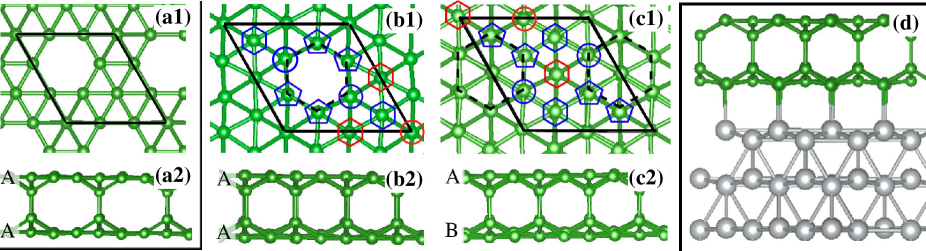
Monolayer borophene. The model for borophene monolayer, BML(), was predicted by Tang et al.,8; 53 as the energetically most stable geometry for single-layer borophene. The BML() phase is characterized by a planar sheet of boron atoms forming a hexagonal pattern of holes with hole density () of 1/9. Its electronic structure is characterized by fully occupied (unoccupied) in-plane () bonding (anti-bonding) states, combined with partially occupied out-of-plane orbitals. A net charge (re)distribution between the three- and two-center bondings8 makes the phase energetically stable. A few years later, Wu et al.10 verified that such a planar structure is dynamically unstable; they found imaginary frequencies in the phonon spectra calculations. However, in the same study, they found that (i) those imaginary frequencies are removed upon vertical buckling of the boron atoms in an alternated fashion, followed by (ii) a slight increase of the borophene binding energy. Indeed, our results confirm that such a buckled structure, BML(), is energetically more stable than the planar BML() by 5 meV/B-atom, followed by a nearly negligible reduction of the lattice constant (less than 0.12 %) when compared with one of the flat () phase, namely 5.029 5.023 Å. In Ref. 10, based on DFT-PBE calculations, the authors obtained equilibrium bond lengths of 5.050 () and 5.046 Å ().
Borophene bilayer. The energetically stable borophene bilayer (BBL) structure, predicted by Wu et al., is characterized by the AA stacking of BML()s connected by one interlayer B-B bond per periodic surface unit cell, Fig. 1(a). As discussed in Ref. 21, the formation of interlayer B–B bonds are mediated by additional electrons resulting from the hollow hexagons on the borophene sheets. In this case, the densities of interlayer bonds () and hollow hexagons are the same, = = 1/9, here refereed as BBL().
| BBL | B-B (Å) | |||
|---|---|---|---|---|
| BBL() | 1/9 | 1/9 | -0.037 | 1.70 |
| BBL | 1/12 | 1/4 | -0.149 | 1.69(1)/1.77(2) |
| BBL | 1/12 | 1/4 | -0.153 | 1.72(2)/1.77(1) |
Recent studies, based on first-principles DFT simulations,55; 22 predicted the formation of energetically and structurally stable hexagonal structures with = 1/12 and = 1/4, hereafter referred to as BBL and BBL, shown in Figs. 1(b) and (c), respectively. In BBL the BML sheets are eclipsed (A-A stacked), while in BBL the borophene layers are staggered (A-B stacking). They found that (i) these two BBL systems present nearly the same total energy, with the latter more stable by 3 meV/B-atom, and (ii) both are energetically more stable than BBL() by about 149 meV/B-atom. Indeed, as shown in Table 1, we found that the total energy of BBL is 4 meV/B-atom lower in comparison with the one of BBL[(i)], and both are energetically more stable than BBL() by about 116 meV/B-atom [(ii)].
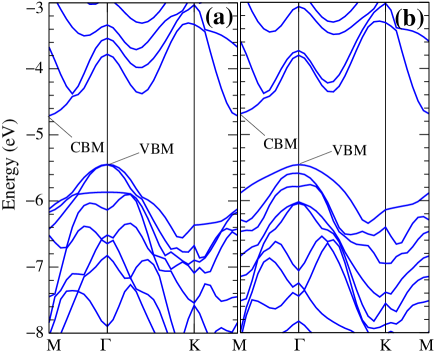
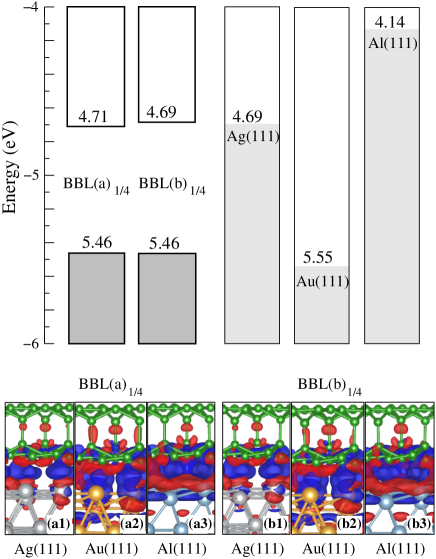
In Figs. 2(a) and (b) we present the electronic band structures of BBL and BBL systems. These BBL systems are semiconductors, with indirect energy gaps () of 0.75 and 0.77 eV, calculated with the GGA-PBE approach. We found the valence (conduction) band maximum (minimum) at the (M) point, resulting in ionization-potential (IP) and electronic-affinity (EA) of 5.46 and 4.71 eV [for BBL], and 5.46 and 4.69 eV [for BBL], which are somewhat comparable with those found in MoS2.56; 57
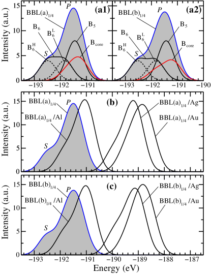
Further structural characterization was carried out through a set of simulations of the B- X-ray photoelectron spectra (XPS). The similarities in the structural and electronic properties of the BBL and BBL are reflected in their XPS results. Indeed, as shown in Figs. 3(a1) and (a2) (shaded region), we find that AA and AB stackings present essentially the same XPS spectrum. However, despite such similarities, it is worth examining the spectral contribution of boron atoms as a function of local geometry and coordination, specifically (i) the spectra B5 of the five-fold coordinated atom [indicated by pentagons in Fig. 1(b1) and (c1)] are characterized by a single peak with a BE of 191.4 eV, thus, indicating that these atoms are at the same structural and chemical environments. In contrast, (ii) the B- electrons of the six-fold coordinated atoms present higher values of BEs, and their spectra (B6) are composed by a superposition of two sub-peaks [dashed lines in Fig. 3(a)] with BEs of about 192.5 (B) and 191.8 eV (B), where the one with the higher (lower) BE is characterized by six (four) next-nearest neighbor (NNN) coordination [red (blue) hexagons in Fig. 1(b1) and (c1)]. (iii) The boron atoms that form the interlayer (vertical) bonds present the lowest values of B- BEs, B [red solid line in Fig. 3(a)]. These core atoms are six- and seven-fold coordinated, as indicated by the blue and red circles in Fig. 1(b1) and (c1), where it is noticeable a slightly larger BE dispersion of B in BBL when compared with that in BBL, Figs. 3(a2) and (a1), respectively.
Finally, it is worth noting that BE’s peak at 191.5 eV results from the superposition of B5 (main contribution), B and B. The five-fold coordinated atoms, which are aside from the hollow hexagons, make the major contribution to the BE peak , followed by the core atoms that form the interlayer B - B bonds, and the six-fold coordinated atoms with four NNN boron atoms. The shoulder , meanwhile, is a BE fingerprint of B from the six-fold coordinated atoms with six NNN boron atoms.
III.2 Borophene on the metal (111) surface
In the sequence, we have studied the energetic properties, structural characterization, electronic, and electronic-transport properties of the BBL adsorbed on the metal surfaces (BBL/m-surf), namely BBL and BBL on the Ag(111), Au(111), and Al(111) surfaces, Fig. 1(d).
III.2.1 Energetic and structural properties
The energetic stability of the BBL/m-surf systems can be determined through the calculation of the binding energy () defined as
where is the total energy of the final system, and and are the total energies of the isolated components, borophene bilayer, and metal surface. We have examined three interface configurations for BBL/Ag(111), namely, with the BBL hexagonal hollow site aligned with (i) bridge, (ii) hollow, and (iii) on-top sites of the Ag(111) surface. We found that (i) is energetically more favorable than (ii) and (iii) by 1.6 and 4.0 meV/Å2, respectively. We have considered the same interface geometry [(i)] for the other BBL/m-surf systems.
| BBL/metal(111) | (Å) | B-B (Å) | |
|---|---|---|---|
| BBL/Ag(111): | |||
| BBL | 2.508 | 1.70(1)/1.79(2) | |
| BBL | 2.427 | 1.74(2)/1.79(1) | |
| BBL/Au(111): | |||
| BBL | 2.272 | 1.71(1)/1.79(2) | |
| BBL | 2.267 | 1.74(2)/1.78(1) | |
| BBL(new2) | 2.250 | 1.74(2)/1.78(1) | |
| BBL/Al(111): | |||
| BBL | 2.428 | 1.71(1)/1.79(2) | |
| BBL | 2.441 | 1.74(2)/1.79(1) |
| BL/metal(111) | (eV) | () |
| BL/Ag(111): | ||
| BBL | 4.777 | |
| BBL | 4.680 | |
| BL/Au(111): | ||
| BBL | 4.632 | |
| BBL | 4.680 | |
| BBL (new2) | 4.658 | |
| BL/Al(111): | ||
| BBL | 4.760 | |
| BBL | 4.721 |
Our binding energy results (Table 2) are comparable with those predicted for other 2D systems, for instance MoS2/Ag(111),26; 58 and can be classified as “potentially exfoliable”.59 Indeed, such an exfoliable nature of BBL adsorbed on Ag(111) was pointed out (very recently) by Xu et al.22, where they found of meV/Å2 using the Grimme formula (vdW-D2), and Li et al.31 where they obtained of 100 meV/Å2 and =2.26 Å using vdW-D3.60 Here, using the same vdW-D2 approach we found a binding energy of meV/Å2. In Table 5 (Appendix) we present our results of binding energy and equilibrium geometry of BBL/Ag(111) obtained using other vdW approaches.
III.2.2 Electron/Hole doping
The energy positions of the ionization potentials (IP) and electronic affinity (EA) of free-standing borophene bilayers, as well as the work function of the pristine (111) metal surfaces (), are shown in Fig. 4 (top-diagram). Our findings of are in good agreement with the experimental results, 61 viz.: = 4.53; = 5.33; = 4.32 eV [Table 3].
When the BBL/m-surf interface forms, there is a net electron transfer from the Ag(111) and Al(111) surfaces to the BBLs, -type doping, whereas in BBL/Au(111) the electron transfer occurs in the opposite direction, and the BBLs become -type doped. The - and -type doping level of the BBLs were examined using the Bader charge density analysis,62 see Table 3. Meanwhile, the net charge transfer profile () along the BBL/m-surf systems, shown in Figs. 4(a) and (b), reveal that the charge transfers [ (blue), and (red)] are localized in the BBL/m-surf interface region.
III.2.3 Structural characterization: XPS
We found that the atomic lattice structures of the BBLs have been retained even though chemical bonds have formed at the BBL/m-surf interface. Indeed, our simulated XPS spectra of the BBL/m-surf systems [Figs. 3(b) and (c)] reveal nearly the same XPS features as those obtained in the free-standing BBLs [Fig. 3(a)]. However, characterized by a reduction of the B- BEs, giving rise to negative values of (B-) core level shifts (CLSs), . For instance, in BBL/Ag(111) [Fig. 3(b)], it is noticeable the reduction of the BE associated with the more intense spectra, BE = 189.2 eV, resulting in a CLS of eV when compared with the energy position of its counterpart (peak ) of pristine BBL [Fig. 3(a1)], and the almost suppression of the shoulder attributed to the BE spectra B. These features were also observed in the other BBL/m-surf systems, with of about and for BBL/Au(111) and /Al(111), Fig. 3(b) and (c), independent of the BBL geometry.
The lowering of the B- core-level BE, , can be qualitatively understood in light of initial state mechanisms, namely (i) net charge transfers, (ii) orbital hybridizations, and (iii) emergence of the external electric fields (EEFs) at the BBL/metal interface.63; 64 Our results indicate that the former two mechanisms play a minor role. For example, the net electron transfers, based on the Bader analysis62 (Table 3) we find that (on average) each boron atom of BBL/m-surf is electron-doped by about 0.007 and 0.014 for m-surf = Ag(111) and Al(111), respectively, whereas in BBL/Au(111) the boron atoms are hole-doped by 0.007 /B-atom. We estimate the B- CLSs induced by such amount of charge transfers (Appendix, see Table 6). The BE of the B5 spectrum is found to be reduced by and eV in the -type doped BBL/Ag(111), and /Al(111), whereas in the -type doped BBL/Au(111), the B BE increases by = eV. In (ii), the Löwdin charge density analysis65 reveals that the formation of the BBL/metal interfaces is characterized by a slight increase in the electron occupation of BBL/metal interface B- orbitals [] in comparison with those of free-standing BBLs. For example, we found of 0.12 /B-atom for the five-fold boron atoms at the BBL/metal interface. These findings suggest that the screening effects induced by the EEFs [(iii)] make the main contribution to the B- CLSs. The emergence of such EEFs is due to the formation of electron- and hole-rich centers localized at the BBL/metal interface, blue and red isosurfaces in Figs. 4(a) and (b), where the negative values of CLSs, , indicate the predominance of electron-repulsive potentials () on the B- core levels.
III.2.4 Electronic band structure
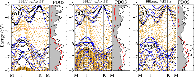
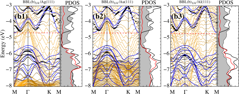
In Figs. 5(a) and (b) we show the electronic band structure of BBL/ and BBL/m-surf, where the electronic band structures of pristine BBL and BBL are indicated in blue solid lines. It is noticeable (i) the formation of metallic bands within the energy gap of the pristine BBLs, and (ii) the absence of localized interface states. The projected density of states (PDOS) on the bottom-most boron atoms (shaded region in Fig. 5) reveal (iii) the emergence of orbital overlaps at the BBL/metal interface, which, in combination with (i) and (ii), may lead to a lowering of the BBL/metal contact resistance. As a result of such orbital overlap and the BBL m-surf net charge transfer, the Fermi level (red dashed lines) is pinned near the CBM of pristine BBLs (blue solid lines); resulting in work functions () between 4.6 and 4.8 eV, almost independent of the metal surface [Table 3]. In contrast, the PDOS of the inner and topmost layers of BBL and BBL, red and black solid lines in Fig. 5, reveal that the semiconducting character is preserved in the BBL’s inner and top layers. The orbital projected band structure on the topmost boron layer (filled circles in Fig. 5) indicates that the CBM lies along the M- direction, which results in a -type Schottky barrier between 0.1 and 0.3 eV. It is important to note that such Schottky barriers are with respect to the topmost and inner layers of BBL; when we consider the bottom-most layer, there is no Schottky barrier; instead, we have a BBL/m-surf ohmic contact due to the metalization of the interface states.
| BL/metal(111) | |||
|---|---|---|---|
| BL/Ag(111): | |||
| BBL | 2.31 | 0.90 | 0.25 |
| BBL | 2.12 | 0.87 | 0.27 |
| BL/Au(111): | |||
| BBL | 1.79 | 0.73 | 0.37 |
| BBL | 1.83 | 0.70 | 0.38 |
| BL/Al(111): | |||
| BBL | 1.67 | 0.80 | 0.35 |
| BBL | 1.66 | 0.80 | 0.35 |
III.2.5 Metal BBL electron tunneling barrier
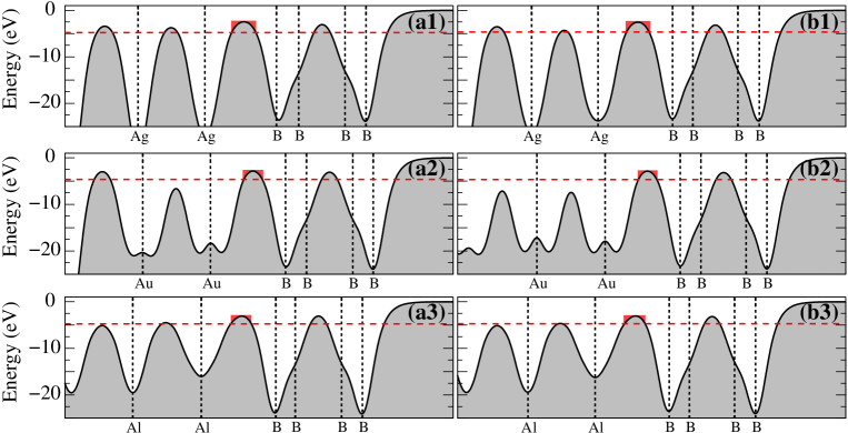
The maintenance of the semiconducting properties in the boron topmost and core layers combined with the formation of metallic channels at the BBL/metal contact region, as reported in (i)-(iii) above, suggest that the BBL/m-surf is a promising platform to be used in the design of electronic devices based on 2D materials. In that sense, the tunneling barrier at the BBL/m-surf interface is an important feature in order to evaluate the electron injection efficiency at the contact region. The averaged electrostatic potential along the BBL/m-surf system (Fig. 6) is characterized by the rise of a tunneling barrier at the interface region. The tunneling probability () is ruled by the height () and the width () of the tunneling barrier. Assuming that the tunneling barrier height is constant () with a rectangular shape and width equal , as indicated by the red shaded regions in Fig. 6, we can infer as,
within the WKB approximation.30; 66; 67 Our results of , presented in Table 4, are comparatively larger than those obtained in septuple-layered MoSi2N4 and WSi2N4 MLs,68 and MoS2 ML and BL58 on Au and Ag surfaces, however smaller than those predicted for phosphorene ML on the same metal surfaces.30
III.2.6 Electronic transport along the BBL channels
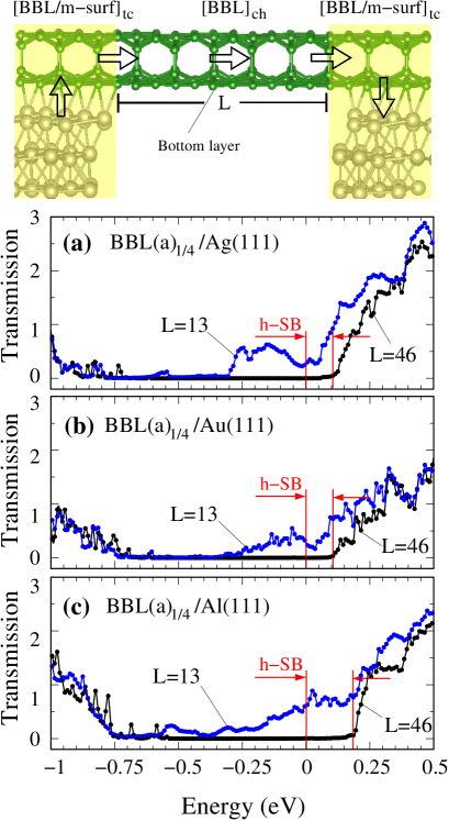
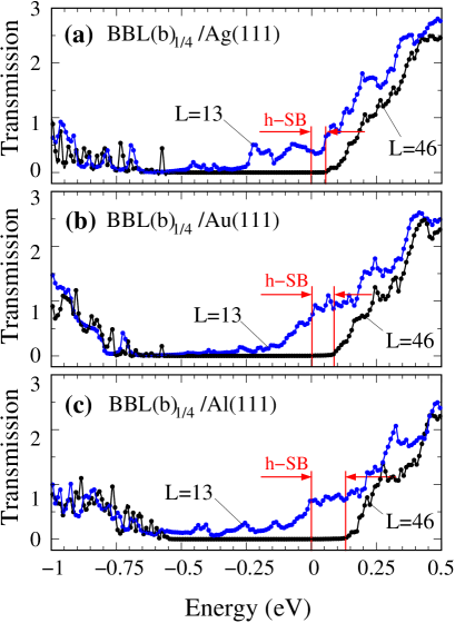
In order to provide a complete picture of BBL as a viable and promising material for “two-dimensional electronics”, we calculate the electronic transmission function, [eq. (1)], taking into account the BBL/m-surf top contact (tc) region connected with the semiconductor BBL channel (ch), [BBL/m-surf] - [BBL] - [BBL/m-surf] schematically shown in the top diagram of Fig. 7. Our results of are depicted in Figs. 7(a)-(c) and 8 for BBL/ and BBL/m-surf contacts, respectively, where we have considered BBL channel lengths (L) of 13 and 46 Å.
For L = 13 Å, we find transmission features with around the Fermi level, which can be attributed to orbital overlaps (predominantly) along the bottom boron layer of [BBL] connecting the left and right contacts, [BBL/m-surf]. By increasing the length of the BBL channel to L = 46 Å such an orbital overlap is suppressed, giving rise to transmission gaps, = 0, around the Fermi level. For instance, in BBL/Ag(111) [Fig. 7(a)] we find = 0 for eV. Meanwhile, increasing the energy window towards positive values, eV, we will find the emergence of electronic transport () mediated by the conduction band of [BBL]. As a result, we find a -type horizontal Schottky barrier (h-SB) of about 0.1 eV between [BBL/Ag(111)] contact and [BBL] channel.
It is worth noting that the transmission gap extends to an energy interval of 0.7 eV below the Fermi level, i.e. = 0 for , resulting in a total transmission gap of about 0.8 eV which is very close to the band-gap of the free-standing BBL. That is, even though orbital hybridizations (metallizations) take place at the BBL/Ag(111) contact interface, the bandgap of BBL (channel) is recovered for L 5 nm.
The electronic transport results in the other systems, Figs. 7(b)-(c) and 8(a)-(c), are somewhat comparable with those obtained for [BBL/Ag(111)] - [BBL] - [BBL/Ag(111)] [Fig. 7(a)], characterized by the formation of an -type h-SB barriers between 0.1 and 0.2 eV almost independent of the BBL geometry. Indeed, this is in consonance with the fact that BBL/m-surf systems present practically the same work function (between 4.6 and 4.8 eV) and BBL and BBL have nearly identical ionization potentials and electron affinity, Fig. 4.
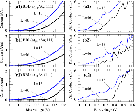
By using the Landauer-Büttiker formula [eq. (2)], we examined the electronic current () and the respective differential-conductance () through the BBL channels with L = 13 and 46 Å. We have considered the limit of low bias voltage, which allows us to estimate the electronic current using the transmission probability at zero-bias. Our results, presented in Fig. 9, show that at the short-channel limit, L = 13 Å, the absence of horizontal Schottky barrier is characterized by the non-zero values of differential conductances, 0. In contrast, for a channel length of L = 46 Å the h-SBs are identified by the voltage intervals () with 0. For example, in the BBL/Ag(111) contact, Fig. 9(a2), we find 0 for up to 0.2 eV, which corresponds to eV with respect to the Fermi level, resulting in an h-SB of 0.1 eV between the BBL/Ag(111) contact and the BBL channel. A similar result was obtained in the BBL/Au(111) contact [Fig. 9(b2)], whereas the h-SB increases to about 0.2 eV when the aluminum contact, BBL/Al(111), is considered [Fig. 9(c2)]. Finally, it is worth mentioning that, when the bias voltage exceeds the h-SB (), the aluminum and silver contacts will promote higher values of differential conductivity, , in comparison with that of the gold contact.
IV Summary and Conclusions
By means of first-principles DFT calculations, we performed a thorough investigation of the electronic and structural properties of borophene bilayer (BBL) in contact with metal surfaces, BBL/m-surf. The formation of BBL/m-surf [with m-surf = Ag, Au, and Al (111) surfaces] is exothermic with binding energies between 30 and 40 meV/Å2, which are comparable with other 2D systems adsorbed on metal surfaces, like MoS2/Ag(111). At the equilibrium geometry, the orbital overlap at the BBL/m-surf interface promote the formation of ohmic BBL/metal contact, and the BBL m-surf net charge transfers result in -type doped BBLs for m-surf = Ag and Al (111) surfaces, and -type doped for BBL/Au(111). Further structural and electronic characterization of the BBL/m-surf interfaces was performed by a set of simulations of the B- X-ray photoelectron spectra (XPS), with the goal of providing support and atomic scale understanding for (future) experimental XPS investigations. Here, we found that the formation of BBL/m-surf is characterized by a red shift of the B- core level spectra when compared with the free-standing BBL. The electronic transport through BBL channels connected to the BBL/m-surf contacts reveals the emergence of a horizontal -type Schottky barrier between 0.1 and 0.2 eV for channels lengths larger than 5 nm. These findings show that borophene bilayers can be an important player in the current research in two-dimensional electronics.
Acknowledgements.
The authors acknowledge financial support from the Brazilian agencies CNPq, INCT-Nanocarbono, INCT-Materials Informatics, FAPEMIG, FAPES(TO-1043/2022), and the LNCC (SCAFMat2), CENAPAD-SP for computer time.| BBL/Ag(111) | (Å) | B-B (Å) | |
|---|---|---|---|
| vdW-DF | 2.427 | 1.74(2)/1.79(1) | |
| vdW-Opt88 | 2.359 | 1.74(2)/1.79(1) | |
| vdW-DF-cx | 2.259 | 1.73(2)/1.78(1) | |
| vdW-D2 | 2.223 | 1.73(2)/1.76(1) |
V Appendix
V.1 Binding energies using other vdW approaches
V.2 B- CLSs of electron/hole doped BBL
In Table 6 we present the calculated B- CLSs of charged () free-standing BBL with respect to neutral system, , where we found that the B- core level BE reduces (increases) upon electron (hole) doping.
| (eV) | ||
|---|---|---|
| /B-atom ( | -type | -type |
| 0.007 (5.1 ) | ||
| 0.014 (10.2) | ||
References
- Novoselov et al. (2004) K. S. Novoselov, A. K. Geim, S. V. Morozov, D. Jiang, Y. Zhang, S. V. Dubonos, I. V. Grigorieva, and A. A. Firsov, “Electric Field Effect in Atomically Thin Carbon Films,” Science 306, 666–669 (2004).
- Radisavljevic et al. (2011) B. Radisavljevic, A. Radenovic, J. Brivio, V. Giacometti, and A. Kis, “Single-layer MoS2 transistors,” Nature Nanotechnology 6, 147–150 (2011).
- Allain et al. (2015) Adrien Allain, Jiahao Kang, Kaustav Banerjee, and Andras Kis, “Electrical contacts to two-dimensional semiconductors,” Nature Materials 14, 1195–1205 (2015).
- Vogt et al. (2012) Patrick Vogt, Paola De Padova, Claudio Quaresima, Jose Avila, Emmanouil Frantzeskakis, Maria Carmen Asensio, Andrea Resta, Bénédicte Ealet, and Guy Le Lay, “Silicene: Compelling Experimental Evidence for Graphenelike Two-Dimensional Silicon,” Phys. Rev. Lett. 108, 155501 (2012).
- Bhimanapati et al. (2015) Ganesh R. Bhimanapati, Zhong Lin, Vincent Meunier, Yeonwoong Jung, Judy Cha, Saptarshi Das, Di Xiao, Youngwoo Son, Michael S. Strano, Valentino R. Cooper, Liangbo Liang, Steven G. Louie, Emilie Ringe, Wu Zhou, Steve S. Kim, Rajesh R. Naik, Bobby G. Sumpter, Humberto Terrones, Fengnian Xia, Yeliang Wang, Jun Zhu, Deji Akinwande, Nasim Alem, Jon A. Schuller, Raymond E. Schaak, Mauricio Terrones, and Joshua A. Robinson, “Recent Advances in Two-Dimensional Materials beyond Graphene,” ACS Nano 9, 11509–11539 (2015).
- Liu et al. (2014) Han Liu, Adam T. Neal, Zhen Zhu, Zhe Luo, Xianfan Xu, David Tománek, and Peide D. Ye, “Phosphorene: An Unexplored 2D Semiconductor with a High Hole Mobility,” ACS Nano 8, 4033–4041 (2014).
- Kunstmann and Quandt (2006) Jens Kunstmann and Alexander Quandt, “Broad boron sheets and boron nanotubes: An ab initio study of structural, electronic, and mechanical properties,” Phys. Rev. B 74, 035413 (2006).
- Tang and Ismail-Beigi (2007) Hui Tang and Sohrab Ismail-Beigi, “Novel Precursors for Boron Nanotubes: The Competition of Two-Center and Three-Center Bonding in Boron Sheets,” Phys. Rev. Lett. 99, 115501 (2007).
- Penev et al. (2012) Evgeni S. Penev, Somnath Bhowmick, Arta Sadrzadeh, and Boris I. Yakobson, “Polymorphism of Two-Dimensional Boron,” Nano Letters 12, 2441–2445 (2012).
- Wu et al. (2012) Xiaojun Wu, Jun Dai, Yu Zhao, Zhiwen Zhuo, Jinlong Yang, and Xiao Cheng Zeng, “Two-Dimensional Boron Monolayer Sheets,” ACS Nano 6, 7443–7453 (2012).
- Mannix et al. (2015) Andrew J. Mannix, Xiang-Feng Zhou, Brian Kiraly, Joshua D. Wood, Diego Alducin, Benjamin D. Myers, Xiaolong Liu, Brandon L. Fisher, Ulises Santiago, Jeffrey R. Guest, Miguel Jose Yacaman, Arturo Ponce, Artem R. Oganov, Mark C. Hersam, and Nathan P. Guisinger, “Synthesis of borophenes: Anisotropic, two-dimensional boron polymorphs,” Science 350, 1513–1516 (2015).
- Feng et al. (2016) Baojie Feng, Jin Zhang, Qing Zhong, Wenbin Li, Shuai Li, Hui Li, Peng Cheng, Sheng Meng, Lan Chen, and Kehui Wu, “Experimental realization of two-dimensional boron sheets, journal=Nature Chemistry,” 8, 563–568 (2016).
- Kiraly et al. (2019) Brian Kiraly, Xiaolong Liu, Luqing Wang, Zhuhua Zhang, Andrew J. Mannix, Brandon L. Fisher, Boris I. Yakobson, Mark C. Hersam, and Nathan P. Guisinger, “Borophene Synthesis on Au(111),” ACS Nano 13, 3816–3822 (2019).
- Kaneti et al. (2022) Yusuf Valentino Kaneti, Didi Prasetyo Benu, Xingtao Xu, Brian Yuliarto, Yusuke Yamauchi, and Dmitri Golberg, “Borophene: Two-dimensional Boron Monolayer: Synthesis, Properties, and Potential Applications,” Chemical Reviews 122, 1000–1051 (2022).
- Gupta et al. (2018) Sunny Gupta, Alex Kutana, and Boris I. Yakobson, “Dirac Cones and Nodal Line in Borophene,” The Journal of Physical Chemistry Letters 9, 2757–2762 (2018).
- Crasto de Lima et al. (2019) F. Crasto de Lima, G. J. Ferreira, and R. H. Miwa, “Orbital Pseudospin-Momentum Locking in Two-Dimensional Chiral Borophene,” Nano Letters 19, 6564–6568 (2019).
- Liu et al. (2018a) Xiaolong Liu, Zhuhua Zhang, Luqing Wang, Boris I. Yakobson, and Mark C. Hersam, “Intermixing and periodic self-assembly of borophene line defects,” Nature Materials 17, 783–788 (2018a).
- Padilha et al. (2016) José Eduardo Padilha, Roberto Hiroki Miwa, and Adalberto Fazzio, “Directional dependence of the electronic and transport properties of 2D borophene and borophane,” Phys. Chem. Chem. Phys. 18, 25491–25496 (2016).
- Silvestre et al. (2019) G. H. Silvestre, Wanderlã L. Scopel, and R. H. Miwa, “Electronic stripes and transport properties in borophene heterostructures,” Nanoscale 11, 17894–17903 (2019).
- Gao et al. (2018) Nan Gao, Xue Wu, Xue Jiang, Yizhen Bai, and Jijun Zhao, “Structure and stability of bilayer borophene: The roles of hexagonal holes and interlayer bonding,” FlatChem 7, 48–54 (2018).
- Liu et al. (2022) Xiaolong Liu, Qiucheng Li, Qiyuan Ruan, Matthew S. Rahn, Boris I. Yakobson, and Mark C. Hersam, “Borophene synthesis beyond the single-atomic-layer limit,” Nature Materials 21, 35–40 (2022).
- Xu et al. (2022) Ying Xu, Xiaoyu Xuan, Tingfan Yang, Zhuhua Zhang, Si-Dian Li, and Wanlin Guo, “Quasi-Freestanding Bilayer Borophene on Ag(111),” Nano Letters 22, 3488–3494 (2022).
- Chen et al. (2022) Caiyun Chen, Haifeng Lv, Ping Zhang, Zhiwen Zhuo, Yu Wang, Chen Ma, Wenbin Li, Xuguang Wang, Baojie Feng, Peng Cheng, Xiaojun Wu, Kehui Wu, and Lan Chen, “Synthesis of bilayer borophene,” Nature Chemistry 14, 25–31 (2022).
- Yang and Sun (2022) Rui Yang and Mengtao Sun, “Bilayer borophene synthesized on Ag(111) film: Physical mechanism and applications for optical sensor and thermoelectric devices,” Materials Today Physics 23, 100652 (2022).
- Chen et al. (2013) Wei Chen, Elton J. G. Santos, Wenguang Zhu, Efthimios Kaxiras, and Zhenyu Zhang, “Tuning the Electronic and Chemical Properties of Monolayer MoS2 Adsorbed on Transition Metal Substrates,” Nano Letters 13, 509–514 (2013).
- Gong et al. (2014) Cheng Gong, Luigi Colombo, Robert M. Wallace, and Kyeongjae Cho, “The Unusual Mechanism of Partial Fermi Level Pinning at Metal–MoS2 Interfaces,” Nano Letters 14, 1714–1720 (2014).
- Kang et al. (2014) Jiahao Kang, Wei Liu, Deblina Sarkar, Debdeep Jena, and Kaustav Banerjee, “Computational Study of Metal Contacts to Monolayer Transition-Metal Dichalcogenide Semiconductors,” Phys. Rev. X 4, 031005 (2014).
- Parto et al. (2021) Kamyar Parto, Arnab Pal, Tanmay Chavan, Kunjesh Agashiwala, Chao-Hui Yeh, Wei Cao, and Kaustav Banerjee, “One-Dimensional Edge Contacts to Two-Dimensional Transition-Metal Dichalcogenides: Uncovering the Role of Schottky-Barrier Anisotropy in Charge Transport across MS2/Metal Interfaces,” Phys. Rev. Appl. 15, 064068 (2021).
- Xu et al. (2015) Yuehua Xu, Jun Dai, and Xiao Cheng Zeng, “Electron-Transport Properties of Few-Layer Black Phosphorus,” The Journal of Physical Chemistry Letters 6, 1996–2002 (2015).
- Pan et al. (2016) Yuanyuan Pan, Yangyang Wang, Meng Ye, Ruge Quhe, Hongxia Zhong, Zhigang Song, Xiyou Peng, Dapeng Yu, Jinbo Yang, Junjie Shi, and Jing Lu, “Monolayer Phosphorene–Metal Contacts,” Chemistry of Materials 28, 2100–2109 (2016).
- Li et al. (2022) Feng Li, Xiangyan Bo, Hong Wu, Ping Liu, Ruifeng Lu, and Yong Pu, “Opposite surface stress induced the distinctly different contact behaviors of monolayer and bilayer borophene on Ag(111),” Applied Surface Science 601, 154093 (2022).
- Mozvashi et al. (2022) Shobair Mohammadi Mozvashi, Mojde Rezaee Givi, and Meysam Bagheri Tagani, “The effects of substrate and stacking in bilayer borophene,” Scientific Reports 12, 13661 (2022).
- NAT (2022) “Contacts in 2D,” Nature Electronics 5, 255–255 (2022).
- Das et al. (2021) Saptarshi Das, Amritanand Sebastian, Eric Pop, Connor J. McClellan, Aaron D. Franklin, Tibor Grasser, Theresia Knobloch, Yury Illarionov, Ashish V. Penumatcha, Joerg Appenzeller, Zhihong Chen, Wenjuan Zhu, Inge Asselberghs, Lain-Jong Li, Uygar E. Avci, Navakanta Bhat, Thomas D. Anthopoulos, and Rajendra Singh, “Transistors based on two-dimensional materials for future integrated circuits,” Nature Electronics 4, 786–799 (2021).
- Shen et al. (2021) Pin-Chun Shen, Cong Su, Yuxuan Lin, Ang-Sheng Chou, Chao-Ching Cheng, Ji-Hoon Park, Ming-Hui Chiu, Ang-Yu Lu, Hao-Ling Tang, Mohammad Mahdi Tavakoli, Gregory Pitner, Xiang Ji, Zhengyang Cai, Nannan Mao, Jiangtao Wang, Vincent Tung, Ju Li, Jeffrey Bokor, Alex Zettl, Chih-I Wu, Tomás Palacios, Lain-Jong Li, and Jing Kong, “Ultralow contact resistance between semimetal and monolayer semiconductors,” Nature 593, 211–217 (2021).
- Giannozzi et al. (2009) Paolo Giannozzi, Stefano Baroni, Nicola Bonini, Matteo Calandra, Roberto Car, Carlo Cavazzoni, Davide Ceresoli, Guido L Chiarotti, Matteo Cococcioni, Ismaila Dabo, Andrea Dal Corso, Stefano de Gironcoli, Stefano Fabris, Guido Fratesi, Ralph Gebauer, Uwe Gerstmann, Christos Gougoussis, Anton Kokalj, Michele Lazzeri, Layla Martin-Samos, Nicola Marzari, Francesco Mauri, Riccardo Mazzarello, Stefano Paolini, Alfredo Pasquarello, Lorenzo Paulatto, Carlo Sbraccia, Sandro Scandolo, Gabriele Sclauzero, Ari P Seitsonen, Alexander Smogunov, Paolo Umari, and Renata M Wentzcovitch, “QUANTUM ESPRESSO: a modular and open-source software project for quantum simulations of materials,” Journal of Physics: Condensed Matter 21, 395502 (2009).
- Perdew et al. (1996) John P. Perdew, Kieron Burke, and Matthias Ernzerhof, “Generalized Gradient Approximation Made Simple,” Phys. Rev. Lett. 77, 3865–3868 (1996).
- Thonhauser et al. (2007) T. Thonhauser, Valentino R. Cooper, Shen Li, Aaron Puzder, Per Hyldgaard, and David C. Langreth, “Van der waals density functional: Self-consistent potential and the nature of the van der waals bond,” Phys. Rev. B 76, 125112 (2007).
- Langreth et al. (2009) D C Langreth, B I Lundqvist, S D Chakarova-Käck, V R Cooper, M Dion, P Hyldgaard, A Kelkkanen, J Kleis, Lingzhu Kong, Shen Li, P G Moses, E Murray, A Puzder, H Rydberg, E Schröder, and T Thonhauser, “A density functional for sparse matter,” Journal of Physics: Condensed Matter 21, 084203 (2009).
- Thonhauser et al. (2015) T. Thonhauser, S. Zuluaga, C. A. Arter, K. Berland, E. Schröder, and P. Hyldgaard, “Spin Signature of Nonlocal Correlation Binding in Metal-Organic Frameworks,” Phys. Rev. Lett. 115, 136402 (2015).
- Klimeš et al. (2009) Jiří Klimeš, David R Bowler, and Angelos Michaelides, “Chemical accuracy for the van der waals density functional,” Journal of Physics: Condensed Matter 22, 022201 (2009).
- Berland and Hyldgaard (2014) Kristian Berland and Per Hyldgaard, “Exchange functional that tests the robustness of the plasmon description of the van der Waals density functional,” Phys. Rev. B 89, 035412 (2014).
- Grimme (2006) Stefan Grimme, “Semiempirical GGA-type density functional constructed with a long-range dispersion correction,” Journal of Computational Chemistry 27, 1787–1799 (2006).
- Monkhorst and Pack (1976) Hendrik J. Monkhorst and James D. Pack, “Special points for Brillouin-zone integrations,” Phys. Rev. B 13, 5188–5192 (1976).
- Brandbyge et al. (2002) Mads Brandbyge, José-Luis Mozos, Pablo Ordejón, Jeremy Taylor, and Kurt Stokbro, “Density-functional method for nonequilibrium electron transport,” Phys. Rev. B 65, 165401 (2002).
- Papior et al. (2017) Nick Papior, Nicolás Lorente, Thomas Frederiksen, Alberto García, and Mads Brandbyge, “Improvements on non-equilibrium and transport Green function techniques: The next-generation transiesta,” Computer Physics Communications 212, 8–24 (2017).
- Junquera et al. (2001) Javier Junquera, Óscar Paz, Daniel Sánchez-Portal, and Emilio Artacho, “Numerical atomic orbitals for linear-scaling calculations,” Phys. Rev. B 64, 235111 (2001).
- Büttiker et al. (1984) M. Büttiker, Y. Imry, and M. Ya. Azbel, “Quantum oscillations in one-dimensional normal-metal rings,” Phys. Rev. A 30, 1982–1989 (1984).
- Pueyo Bellafont et al. (2015a) Noèlia Pueyo Bellafont, Paul S. Bagus, and Francesc Illas, “Prediction of core level binding energies in density functional theory: Rigorous definition of initial and final state contributions and implications on the physical meaning of Kohn-Sham energies,” The Journal of Chemical Physics 142 (2015a), 10.1063/1.4921823, 214102.
- García-Gil et al. (2012) S. García-Gil, A. García, and P. Ordejón, “Calculation of core level shifts within DFT using pseudopotentials and localized basis sets,” The European Physical Journal B 85, 239 (2012).
- Takahashi and Pettersson (2004) Osamu Takahashi and Lars G. M. Pettersson, “Functional dependence of core-excitation energies,” The Journal of Chemical Physics 121, 10339–10345 (2004).
- Rastogi et al. (2019) Pankaj Kumar Rastogi, Krishna Rani Sahoo, Pallavi Thakur, Rahul Sharma, Sumit Bawari, Ramakrishna Podila, and Tharangattu N. Narayanan, “Graphene–hBN non-van der Waals vertical heterostructures for four- electron oxygen reduction reaction,” Phys. Chem. Chem. Phys. 21, 3942–3953 (2019).
- Tang and Ismail-Beigi (2010) Hui Tang and Sohrab Ismail-Beigi, “First-principles study of boron sheets and nanotubes,” Phys. Rev. B 82, 115412 (2010).
- (54) is defined as the the total energy difference between the BBL (BBL or BBL) and the BML(), , where is the number of boron atoms per unit cell.
- Ma et al. (2022) Yuan-Yuan Ma, Xiao-Yun Zhao, Wenyan Zan, Yuewen Mu, Zhuhua Zhang, and Si-Dian Li, “Prediction of freestanding semiconducting bilayer borophenes,” Nano Research 15, 5752–5757 (2022).
- Jiang (2012) Hong Jiang, “Electronic Band Structures of Molybdenum and Tungsten Dichalcogenides by the GW Approach,” The Journal of Physical Chemistry C 116, 7664–7671 (2012).
- Schlaf et al. (1999) R. Schlaf, O. Lang, C. Pettenkofer, and W. Jaegermann, “Band lineup of layered semiconductor heterointerfaces prepared by van der Waals epitaxy: Charge transfer correction term for the electron affinity rule,” Journal of Applied Physics 85, 2732–2753 (1999).
- Zhong et al. (2016) Hongxia Zhong, Ruge Quhe, Yangyang Wang, Zeyuan Ni, Meng Ye, Zhigang Song, Yuanyuan Pan, Jinbo Yang, Li Yang, Ming Lei, Junjie Shi, and Jing Lu, “Interfacial Properties of Monolayer and Bilayer MoS2 Contacts with Metals: Beyond the Energy Band Calculations,” Scientific Reports 6, 21786 (2016).
- Mounet et al. (2018) Nicolas Mounet, Marco Gibertini, Philippe Schwaller, Davide Campi, Andrius Merkys, Antimo Marrazzo, Thibault Sohier, Ivano Eligio Castelli, Andrea Cepellotti, Giovanni Pizzi, and Nicola Marzari, “Two-dimensional materials from high-throughput computational exfoliation of experimentally known compounds,” Nature Nanotechnology 13, 246–252 (2018).
- Ehrlich et al. (2011) Stephan Ehrlich, Jonas Moellmann, Werner Reckien, Thomas Bredow, and Stefan Grimme, “System-Dependent Dispersion Coefficients for the DFT-D3 Treatment of Adsorption Processes on Ionic Surfaces,” ChemPhysChem 12, 3414–3420 (2011).
- Derry et al. (2015) Gregory N. Derry, Megan E. Kern, and Eli H. Worth, “Recommended values of clean metal surface work functions,” Journal of Vacuum Science & Technology A 33 (2015), 10.1116/1.4934685, 060801.
- Bader (1990) R. Bader, Atoms in Molecules: A Quantum Theory (Oxford University Press, New York, 1990).
- Bagus et al. (1999) Paul S Bagus, Francesc Illas, Gianfranco Pacchioni, and Fulvio Parmigiani, “Mechanisms responsible for chemical shifts of core-level binding energies and their relationship to chemical bonding,” Journal of Electron Spectroscopy and Related Phenomena 100, 215–236 (1999).
- Pueyo Bellafont et al. (2015b) Noèlia Pueyo Bellafont, Paul S. Bagus, and Francesc Illas, “Prediction of core level binding energies in density functional theory: Rigorous definition of initial and final state contributions and implications on the physical meaning of Kohn-Sham energies,” The Journal of Chemical Physics 142 (2015b), 10.1063/1.4921823, 214102.
- Löwdin (2004) Per‐Olov Löwdin, “Approximate Formulas for Many‐Center Integrals in the Theory of Molecules and Crystals,” The Journal of Chemical Physics 21, 374–375 (2004).
- Liu et al. (2018b) Jie Liu, Yaguang Guo, Fancy Qian Wang, and Qian Wang, “TiS3 sheet based van der Waals heterostructures with a tunable Schottky barrier,” Nanoscale 10, 807–815 (2018b).
- Liu et al. (2021) Yan Liu, Qiang Zhang, Wendong Zhang, Riguang Zhang, Baojun Wang, Chao Ji, Zhen Pei, and Shengbo Sang, “Tuning Schottky Barrier and Contact Type of Metal–Semiconductor in Ti3C2T2/MoS2 (T = F, O, OH) by Strain: A First-Principles Study,” The Journal of Physical Chemistry C 125, 16200–16210 (2021).
- Wang et al. (2021) Qianqian Wang, Liemao Cao, Shi-Jun Liang, Weikang Wu, Guangzhao Wang, Ching Hua Lee, Wee Liat Ong, Hui Ying Yang, Lay Kee Ang, Shengyuan A. Yang, and Yee Sin Ang, “Efficient Ohmic contacts and built-in atomic sublayer protection in MoSi2N4 and WSi2N4 monolayers,” npj 2D Materials and Applications 5, 71 (2021).