Supplementary Material for “Layer Construction of Three-Dimensional Monopole Charge Nodal Line Semimetals and Prediction of Abundant Candidate Materials”
I Symmetry consideration
In our layer construction scheme, it is important to utilize the nonsymmorphic symmetry operators, i.e. screw symmetry and slide symmetry, to engineer the parity pattern at time-reversal invariant momentums (TRIMs). In the following, we will consider these nonsymmorphic symmetry operators one by one.
I.1 Twofold screw symmetry
We have claimed in the text that the twofold screw symmetry can be replaced by another symmetry , i.e., a twofold rotation whose rotation axis is perpendicular to and following by a translation . Here we consider the case of and the result for can be immediately obtained by removing the limitation that is normal to and .
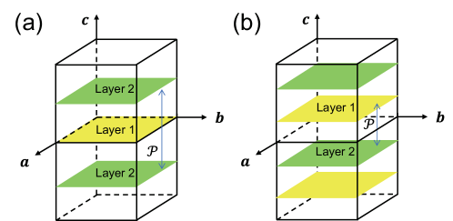
There are two layers of 2D DSMs per unit cell. The 3D structure should also have and there are two ways to restore as shown in Figs. S1 (a) and (b), i.e., two layers are invariant under and exchanges two layers, respectively. And we discuss them separately.
I.1.1 2D layers invariant under
We first consider the case that two layers are invariant under as shown in Fig. S1(a). acts in real space as
| (S1) |
where and are the length of three lattice vectors.
Firstly, we prove that the values of and can only be 0 and 1. Let us consider the restriction of the inversion symmetry of the 3D structure on the positions of inversion centers of each 2D layer. Suppose one of the inversion centers of layer 1 is given by (0,0,0). Performing to (0,0,0), we obtain the corresponding inversion center of layer 2 at the top: . Performing to (0,0,0), we obtain the corresponding inversion center of layer 2 at the bottom: . In the most general case, can only exchange these two inversion centers, i.e.,
| (S2) |
where denotes that the two sides are equal modulo a lattice vector. Therefore, the values of are restricted to . We get the same result by choosing other inversion centers of layer 1, i.e., , , and .
Next, we prove that the atoms in the 3D structure also have inversion symmetry. Here, is still one of the inversion centers of the 3D structure and the 2D layer 1. Consider an arbitrary atom in the layer 2 located at where is the coordinate of an inversion center given by Eq. S2. Since the values of are limited to , and differ only by a lattice vector and is also an inversion center of layer 2. By the translation invariance, there is an equivalent atom at . By the inversion symmetry of the 2D layer 2, the atom of the layer 2 at has an equivalent atom of the layer 2 at . (Recall that is also an inversion center.) Therefore, for every atom in layer 2 on the bottom, there exists an atom in layer 2 on the top that the two atoms ( and ) form an -reversed pair.
However, this is true only when the 2D DSMs do not have . Let us consider 2D DSMs with . In this case, two-fold rotation/screw axes may be , , , or . As a result, followed by acts in real space as
| (S3) |
i.e., the two layers only differ by a pure translation and thus the primitive cell actually contains only one layer of the 2D DSM.
I.1.2 2D layers exchanged under
We now consider the case that exchanges two 2D layers as shown in Fig. S1(b). In this section, we choose a gauge that acts in real space as
| (S4) |
i.e., the twofold screw axis becomes .
Here, we prove that the 3D structure can not have inversion symmetry in the most general case. Assume there is an atom of layer 1 at where is the coordinate of an inversion center of layer 1. Again, there should be an equivalent atom at . Performing on , we have
| (S5) |
For the most general case, we can not find a -reversed pair for every two atoms. However, things become different when the 2D DSMs have . In that case, can only be 0 due to the presence of and in a single layer. Therefore, for an atom at , there is always an atom at . But, in this case, does not commutate or anticommutate with at TRIMs, which will be clear in Sec. II.
I.2 Slide symmetry
In the case of the slide symmetry, while the fundamental symmetries of the 2D DSMs are still time reversal and inversion , additional symmetries are needed. First of all, we need to deal with the commensurability between two layers as shown in Fig. S2(b). Even if the two layers are commensurate, we also need to consider the possible intervalley scattering, which may gap the Dirac cones.
If the above problem does not exist, we still consider two cases as shown in Fig. S1. Without loss of generality, we assume that Dirac cones are located at axis and use as an example in this section. Again, one should notice that the axis does not need to be perpendicular to and as in the case of .
I.2.1 2D layers invariant under
Consider the case that two layers are invariant under as shown in Fig. S1(a). acts in real space as
| (S6) |
where is the mirror plane of the slide symmetry operator and are the length of three lattice vectors.
First, we identify the constraints imposed by the positions of Dirac cones. Consider a pair of Dirac cones at and , then the allowed mirror planes are in momentum space and in real space.
Next, we identify the constraints imposed by the inversion symmetry. Suppose one of the inversion centers of layer 1 is given by (0,0,0). Performing to (0,0,0), we obtain the corresponding inversion center of layer 2 at the top: . Performing to (0,0,0), we obtain the corresponding inversion center of layer 2 at the bottom: . In the most general case, can only exchange these two inversion centers, i.e.,
| (S7) |
where denotes that the two sides are equal modulo a lattice vector. Therefore, the values of are restricted to . We get the same result by choosing other inversion centers of layer 1, i.e., , , or . By similar steps in Sec.I.1.1, we can also prove that the atoms in the 3D structure also have inversion symmetry.
However, we need to take the shape of Dirac cones into account. In the case of , there is no need to care about the shape of the Dirac cones for the following reason. At plane, the inversion symmetry is equivalent to and the inversion symmetry can exchange the -reversed pair of Dirac cones without changing the band structure. As a result, can also exchange the -reversed pair of Dirac cones without changing the band structure at plane. As is just on plane, exchanges the -reversed pair of Dirac cones without changing the band structure at plane. When the interlayer coupling is not considered, there is no energy dispersion in -direction and the band structures of the two layers overlap completely. Since strong interlayer coupling will destroy the NLs, we only consider weak interlayer coupling in the whole momentum space, which will not drastically change the band structure. However, we can not find such a relation between inversion symmetry and mirror symmetry. Thus, slide symmetry can not ensure the complete overlapping of the -reversed pair of Dirac cones and NLs are less likely to appear.
Finally, let us consider 2D DSMs with mirror symmetry. In this case, followed by acts in real space as
| (S8) |
i.e., the two layers only differ by a pure translation , and thus the primitive cell contains only one layer of 2D DSM.
I.2.2 2D layers exchanged under
Consider the case that exchanges two 2D layers as shown in Fig. S1(b). In this section, we choose a gauge that acts in real space as
| (S9) |
i.e., the mirror plane becomes .
Here, we prove that the 3D structure can not have inversion symmetry in the most general case. Assume there is an atom of layer 1 at where is the coordinate of an inversion center of layer 1. Performing on , we have
| (S10) |
In general, we can not find a -reversed pair for every two atoms.
I.3 Other screw symmetries
I.3.1
Since, generally, does not commutate or anticommutate with at TRIMs, we exclude this symmetry.
I.3.2 and
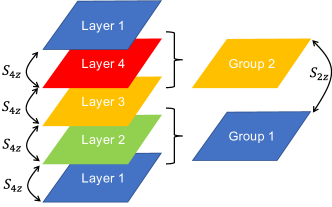
We can group the layers into 2 groups, i.e., two layers in a group for as shown in Fig. S3 and three layers in a group for . What is special in these two cases is that we need to consider the commensurability between layers in a group and the corresponding intervalley scatterings. After that, a group can be regarded as the 2D layer in , and this 2D layer should have inversion symmetry and time reversal symmetry but not . Then the analyses of can be performed similarly.
II Derivation of commutation or anticommutation relation between and in the Wannier representation
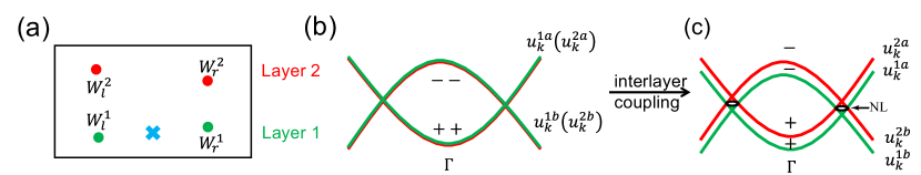
In the derivation of the relation between and , we only consider bands that contribute to the NL, i.e., four bands as shown in Figs. S4(b),(c). And we also limit ourselves to only four Wannier functions in a unit cell as shown in Fig. S4(a). These limitations are not essential and can be easily removed.
Firstly, we derive the transformation of the wannier functions under and using the notations of Refs.[1, 2]. For ,
| (S11) | ||||
Similarly,
| (S12) |
For ,
| (S13) | ||||
Similarly,
| (S14) | ||||
where . Because we obtain a in a different unit cell by performing to a , appears in the equation to move back to the same unit cell with .
Next, we derive the eigenvalues of the four wavefunctions. Consider the 3D structure when the interlayer coupling is absent and the band structure is shown in Fig. S4(b). Suppose and are induced only by obitals in layer 1, and and are induced only by obitals in layer 2. Then we have
| (S15) | ||||
where now is a Bravais lattice vector. We find the parity eigenvalues of these wavefunctions by performing on them. Since we only care about the parity eigenvalues at TRIMs, in the rest of this section and the next section, the momentum is restricted to TRIMs without explicitly specifying.
| (S16) | ||||
When moving into the fourth line, we have used . Similarly,
| (S17) |
Therefore, at all TRIMs, the parity eigenvalue of is 1 and the parity eigenvalue of is -1.
| (S18) | ||||
Similarly,
| (S19) |
Then, we derive the relationship between the wavefunctions. Perform on ,
| (S20) | ||||
where . When moving into the fifth line, we have used . Similarly,
| (S21) |
For this reason, we claimed in the main text that and are two different states.
Finally, we derive the commutation or anticommutation relation between and . For and ,
| (S22) | ||||
For and ,
| (S23) | ||||
In both cases, we have
| (S24) |
or,
| (S25) |
which is just Eq. 1 in the main text.
This relation can also be understood in a more general way as in the main text. The acts in real space as
| (S26) |
and acts in real space as
| (S27) |
Consider the commutation or anticommutation relation between and
| (S28) |
| (S29) |
from which we obtain
| (S30) | ||||
At TRIMs where commutates with , i.e., . By applying to and , we can obtain and , respectively. That is, if there is an occupied state with a certain parity, there exists another occupied state with the same parity. At TRIMs where anticommutates with , i.e., . If there is an occupied state with a certain parity, there exists another occupied state with a different parity.
III All possible parity patterns of the 3D NLSMs from the 2D Dirac SMs
In this section, we explicitly show all possible parity patterns for which the appearance of NLs is allowed.
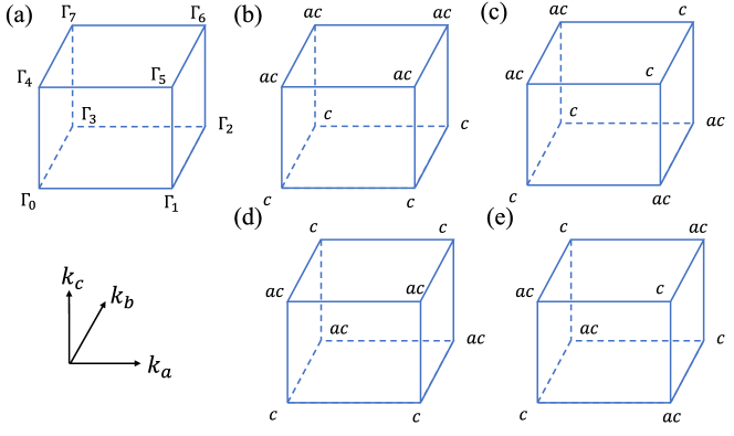
The eight TRIMs are named by , and the coordinates of the are shown in Fig. S5(a) with . The value of when the 2D DSMs does not have are restricted to four cases, i.e. . Correspondingly, according to
| (S31) |
the commutation or anticommutation relations between and at TRIMs are shown in Figs. S5(b-e) for the four cases.

Then we consider a 2D DSM with a parity pattern as shown in Fig. S6(a). We stack the 2D DSM into a 3D NLSM with only one layer per unit cell whose parity pattern (The occupied one of or .) is shown in Fig. S6(b). Here we assume the absence of interlayer coupling. The parity eigenvalues can be obtained from Eq. S16 and Eq. S17. Then we need to find the parity eigenvalues of bands from another layer, i.e., the parity eigenvalues of the occupied one among and .
To this end, we first find out the commutation or anticommutation relation between and at all eight TRIMs as shown in Fig. S5. The two parity eigenvalues of the occupied bands are the same if commutates with and are opposite if anticommutates with , as explained under Eq. S30. As shown in Fig. S6(c), the first parity eigenvalues in the parentheses are the parity eigenvalues of the occupied one of or and the second parity eigenvalues in the parentheses are the parity eigenvalues of the occupied one of or . We then diagnose NLs from the parity pattern by
| (S32) |
If , then the appearing of NLs is allowed. Thus, there should be an odd number of double band inversions (two occupied states with both -1 parity eigenvalues). A double band inversion appears when the first parity eigenvalue in the parentheses is -1 and commutates with at that TRIM.
IV More details on the tight-binding model
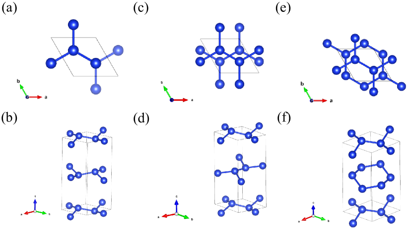
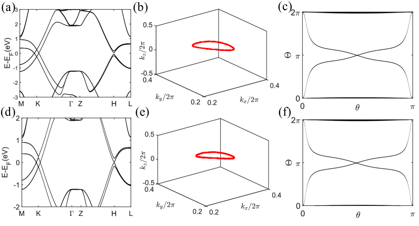
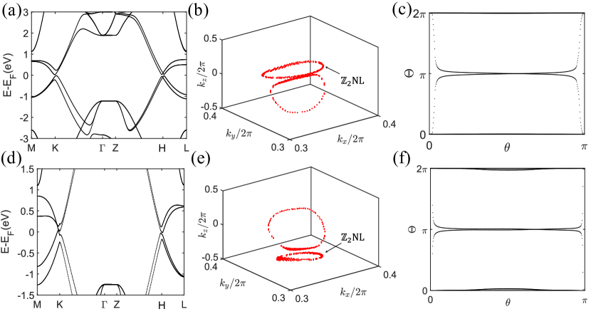
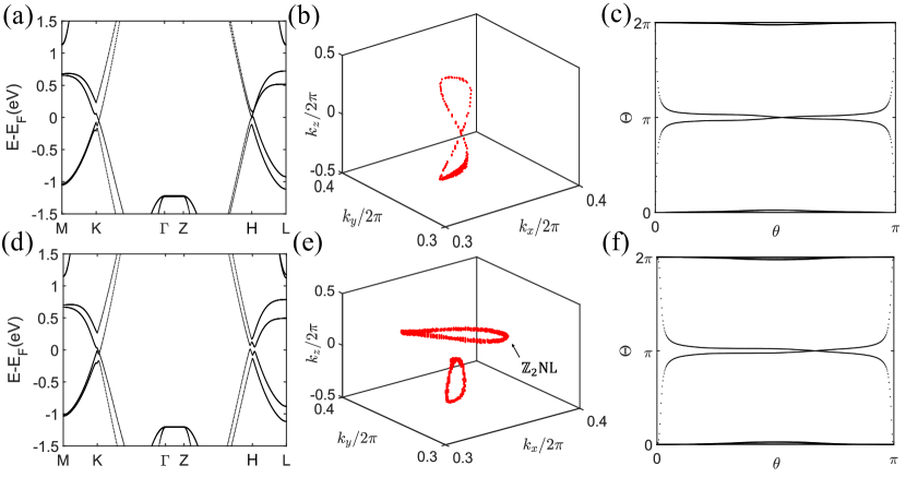
The tight-binding model of the 2D Dirac semimetal we use in the text originates from the tight-binding model of the silicene, i.e., buckled honeycomb lattice, with only orbitals[3]. In this section, we give four models with their nodal surfaces or NLs shown in Figs. S7(e-h). The first model which has spindle-shaped nodal surfaces (Fig. S7(e)) is just due to the supercell effect. The rest models with the same parity patterns give three types of NLs (Fig.S7(f-h)), while only one of them has nontrivial monopole charge (Fig.S7(g)).
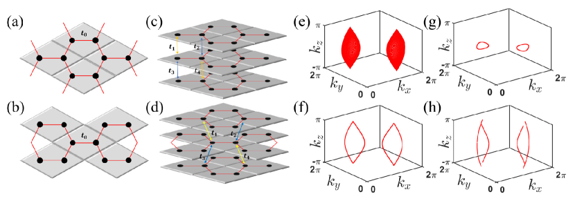
As shown in Fig .S7(c), we choose a screw axis so that it is coincident with the inversion center at or , i.e., or . The three basis lattice vectors are given by
| (S33) |
There are four orbitals in the unit cell and their reduced coordinates are given by
| (S34) | ||||
The Hamiltonian without interlayer coupling reads
| (S35) |
where and , are Pauli matrices and denote sublattice and interlayer degrees of freedom, respectively.
We first assume . As shown in Fig. S7(e), we obtain a pair of spindle-shaped nodal surfaces related by when the interlayer coupling is weak. This can be understood as follows. First, there is a pair of Dirac points in 2D DSM which are related by . The pure translation operator does not change the position of the two Dirac points in momentum space while the twofold rotation operator exchanges the position of the two Dirac points in momentum space. So, now we have a pair of 3D four-fold degenerate Dirac points. When there is no interlayer coupling, the bands have no dispersion in the direction, i.e., the pair of Dirac points become a pair of Dirac NLs in the direction. Then we consider the interlayer coupling term
| (S36) |
which commutates with . The energy dispersion of the Hamiltonian is given by
| (S37) |
The Dirac nodal line above can be regarded as a series of Dirac points and the series of Dirac points become a series of Weyl rings except at where with added. As a result, we get a pair of spindle-shaped nodal surfaces related by , as plotted in Fig. S7(e).
Then we set and consider the interlayer coupling term
| (S38) |
which anticommutates with . The Hamiltonian reads
| (S39) |
The energy dispersion is
| (S40) |
When the values of are small enough, adding to would gap all the degenerate points of the nodal surfaces in Fig. S7(e) except the degenerate points on , i.e., only a pair of NLs on is left as shown in Fig. S7(g).
Next, we consider the case the screw axis coincides with the inversion center at or , i.e., or . While the lattice vectors are the same as Eq. S33, the reduced coordinates of the four orbitals are given by
| (S41) | ||||
as shown in Fig .S7(d).
The Hamiltonian without interlayer coupling is still in Eq. S35. We assume and consider the interlayer coupling term
| (S42) |
where anticommutates with and commutates with . The Hamiltonian is
| (S43) |
Adding to , we obtain a pair of NLs as plotted in Fig. S7(f) since only degenerate points on the plane in a spindle-shaped nodal surface similar to Fig. S7(e) still exist. Since we can not find a 2D closed manifold, like a sphere, enclosing the NL, the monopole charge is ill-defined for such NLs.
Finally, we set and consider the interlayer coupling term
| (S44) |
and the Hamiltonian is
| (S45) |
We can obtain two pairs of NLs as shown in Fig. S7(h) and this kind of NLs do not carry monopole charges, either.
V Detailed results and calculation details about material candidates
Our prediction of material candidates is based on the DFT methods using the PBE form for the GGA as implemented in the Vienna ab initio simulation package (VASP)[4]. The Gamma scheme -point mesh size is set to for transition metal dichalcogenides (TMDs) and for wurtzite Si/Ge and the plane-wave cutoff energy is set to 500 eV. The lattice structure is optimized until the forces on the atoms are less than 0.002 eV/. Then a model is constructed using wannier90[5]. We use both parity analysis and the Wilson loop method to verify the nontrivial monopole charges of the nodal lines.
V.1 TMDs
As has been grown in experiments, we first perform structure optimization on it to verify our calculation parameters. We find that the vdW correction is not needed and the lattice structure of the experiments and lattice structure after structure optimization is shown in Table. S1. Thus, in the following calculations, we do not consider the vdW corrections.
| Experiments | Structure optimization | |||||
|---|---|---|---|---|---|---|
| Element | x | y | z | x | y | z |
| Te | 0.581 | 0.750 | 0.595 | 0.576 | 0.750 | 0.594 |
| Te | 0.419 | 0.250 | 0.405 | 0.424 | 0.250 | 0.406 |
| Te | 0.091 | 0.250 | 0.633 | 0.088 | 0.250 | 0.631 |
| Te | 0.909 | 0.750 | 0.367 | 0.912 | 0.750 | 0.369 |
| Te | 0.564 | 0.250 | 0.867 | 0.568 | 0.250 | 0.869 |
| Te | 0.436 | 0.750 | 0.133 | 0.432 | 0.750 | 0.131 |
| Te | 0.062 | 0.750 | 0.905 | 0.062 | 0.750 | 0.906 |
| Te | 0.938 | 0.250 | 0.095 | 0.938 | 0.250 | 0.094 |
| Mo | 0.182 | 0.750 | 0.506 | 0.182 | 0.750 | 0.506 |
| Mo | 0.818 | 0.250 | 0.493 | 0.818 | 0.250 | 0.494 |
| Mo | 0.320 | 0.250 | 0.007 | 0.319 | 0.250 | 0.006 |
| Mo | 0.680 | 0.750 | 0.993 | 0.681 | 0.750 | 0.994 |
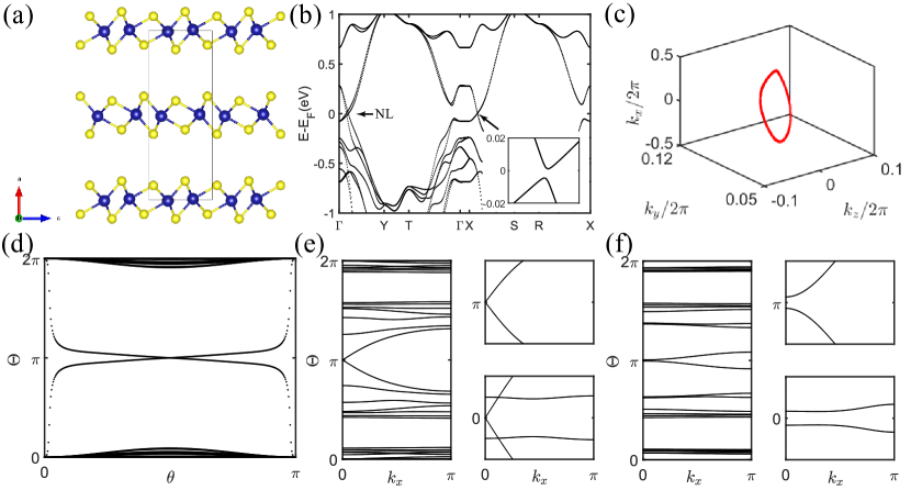
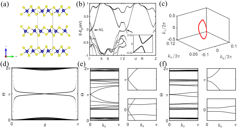
For the 3D counterparts of 2D (=Cr,Mo,W, =S,Se,Te), there are 9 possible element combinations and 16 spatial structures for each combination, a total of 144 3D TMDs. For each of the four combinations of , we have one structure for ( phase), i.e., is perpendicular to both and , and three structures for ( phase), i.e., is inclined towards the -axis, is inclined towards the -axis, and is inclined towards both the -axis and -axis. We find all the structures in the phase and two out of three structures in the phase have NLs, as shown in Table. S2, a total of 108 3D TMDs. Although the 12 spatial structures with NLs are structurally different, they share the same parity feature as in Table. S3.
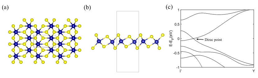
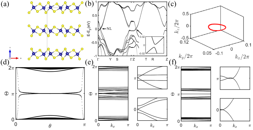
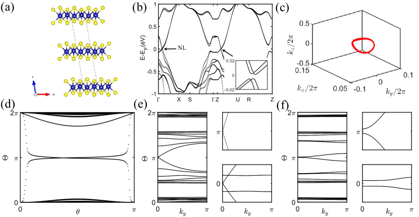
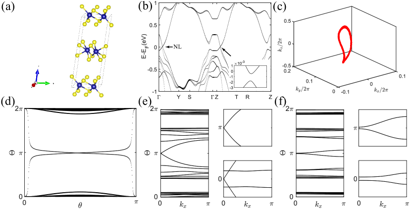
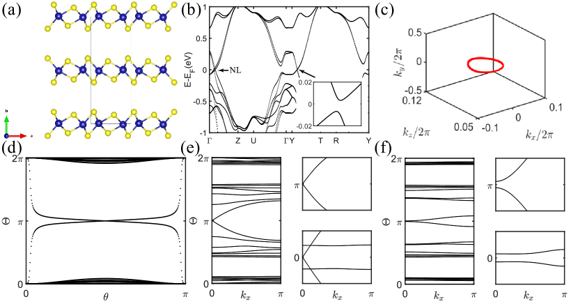
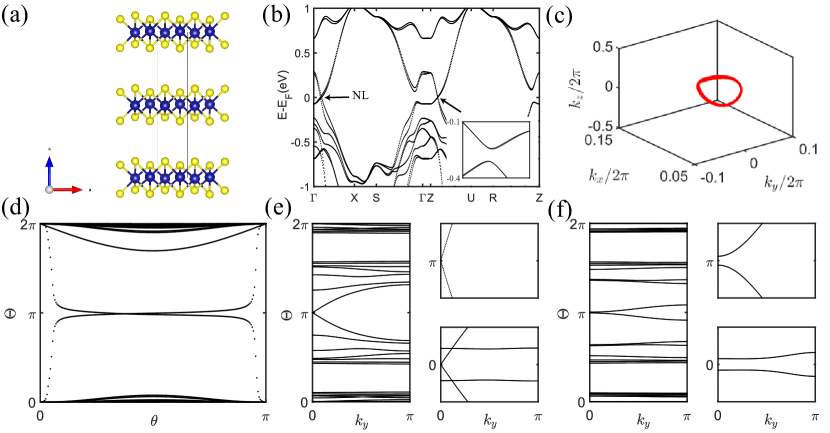
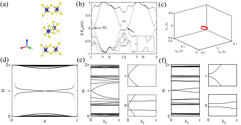
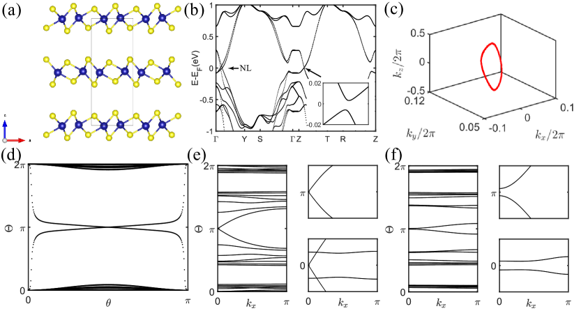
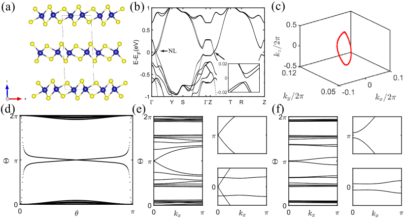
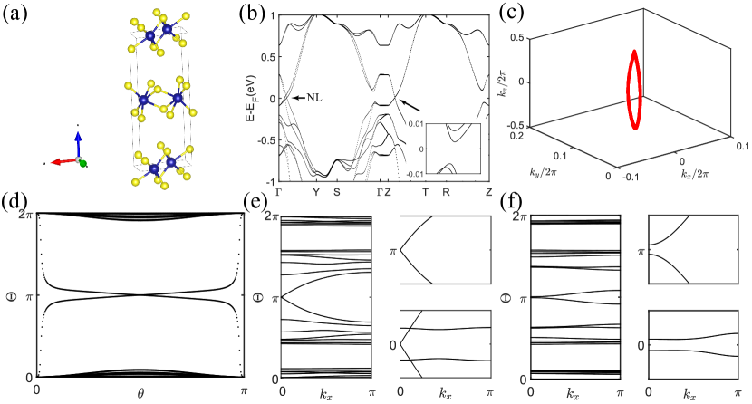
Here we just show the results for and other materials that have similar band structures. The lattice structure of monolayer is shown in Figs .S8(a)(b). The monolayer has a -reversed pair of Dirac points along .
| & | & | & | & | |
|---|---|---|---|---|
| (0,0) | crystal 1 (SG.59) | crystal 2 (SG.13) | (SG.11) | crystal 3 (SG.2) |
| (0,1) | crystal 4 (SG.57) | crystal 5 (SG.13) | (SG.11) | crystal 6 (SG.2) |
| (1,0) | crystal 7 (SG.62) | (SG.14) | crystal 8 (SG.11) | crystal 9 (SG.2) |
| (1,1) | crystal 10 (SG.62) | crystal 11 (SG.14) | (SG.11) | crystal 12 (SG.2) |
| =0 | ||||||||
|---|---|---|---|---|---|---|---|---|
| TRIM | X | Y | Z | S | T | U | R | |
| 22 | 24 | 24 | 24 | 24 | 24 | 24 | 24 | |
V.1.1
Crystal 1 is the Td phase, and the rest two structures are the phase. Crystal 2 can be gotten by changing the angle between and axes in crystal 1, i.e., the two layers have undergone a relative displacement in the -direction. Crystal 3 can be gotten by changing the angles between both and axes and and axes in crystal 1, i.e., the two layers have undergone a relative displacement in both and -directions.
| crystal 1 | crystal 2 | crystal 3 | |||||||
|---|---|---|---|---|---|---|---|---|---|
| Element | x | y | z | x | y | z | x | y | z |
| Cr | 0.197 | 0.250 | 0.495 | 0.197 | 0.755 | 0.005 | 0.200 | 0.251 | 0.995 |
| Cr | 0.803 | 0.750 | 0.505 | 0.803 | 0.245 | 0.995 | 0.800 | 0.749 | 0.005 |
| Cr | 0.803 | 0.750 | 0.995 | 0.803 | 0.755 | 0.505 | 0.305 | 0.251 | 0.495 |
| Cr | 0.197 | 0.250 | 0.005 | 0.197 | 0.245 | 0.495 | 0.695 | 0.749 | 0.505 |
| S | 0.924 | 0.250 | 0.892 | 0.924 | 0.347 | 0.608 | 0.474 | 0.766 | 0.388 |
| S | 0.076 | 0.750 | 0.108 | 0.076 | 0.653 | 0.392 | 0.526 | 0.234 | 0.611 |
| S | 0.425 | 0.750 | 0.918 | 0.425 | 0.824 | 0.582 | 0.964 | 0.262 | 0.414 |
| S | 0.575 | 0.250 | 0.082 | 0.575 | 0.176 | 0.418 | 0.036 | 0.738 | 0.585 |
| S | 0.076 | 0.750 | 0.392 | 0.076 | 0.347 | 0.108 | 0.128 | 0.766 | 0.888 |
| S | 0.924 | 0.250 | 0.608 | 0.924 | 0.653 | 0.892 | 0.872 | 0.234 | 0.112 |
| S | 0.575 | 0.250 | 0.418 | 0.575 | 0.824 | 0.082 | 0.615 | 0.262 | 0.915 |
| S | 0.425 | 0.750 | 0.582 | 0.425 | 0.176 | 0.918 | 0.385 | 0.738 | 0.085 |
V.1.2
Crystal 4 is the Td phase, and the rest two structures are the phase. Crystal 5 can be gotten by changing the angle between and axes in crystal 4, i.e., the two layers have undergone a relative displacement in the -direction. Crystal 6 can be gotten by changing the angles between both and axes and and axes in crystal 4, i.e., the two layers have undergone a relative displacement in both and -directions.
| crystal 4 | crystal 5 | crystal 6 | |||||||
|---|---|---|---|---|---|---|---|---|---|
| Element | x | y | z | x | y | z | x | y | z |
| Cr | 0.803 | 0.250 | 0.995 | 0.803 | 0.750 | 0.505 | 0.804 | 0.250 | 0.00510 |
| Cr | 0.197 | 0.750 | 0.005 | 0.197 | 0.250 | 0.495 | 0.196 | 0.750 | 0.99490 |
| Cr | 0.197 | 0.250 | 0.495 | 0.197 | 0.750 | 0.005 | 0.199 | 0.250 | 0.50507 |
| Cr | 0.803 | 0.750 | 0.505 | 0.803 | 0.250 | 0.995 | 0.801 | 0.751 | 0.49493 |
| S | 0.076 | 0.750 | 0.388 | 0.076 | 0.254 | 0.112 | 0.109 | 0.743 | 0.61225 |
| S | 0.924 | 0.250 | 0.612 | 0.924 | 0.746 | 0.888 | 0.891 | 0.257 | 0.38775 |
| S | 0.575 | 0.250 | 0.415 | 0.575 | 0.753 | 0.085 | 0.599 | 0.245 | 0.58569 |
| S | 0.425 | 0.750 | 0.585 | 0.425 | 0.247 | 0.915 | 0.401 | 0.755 | 0.41431 |
| S | 0.924 | 0.750 | 0.888 | 0.924 | 0.254 | 0.612 | 0.953 | 0.743 | 0.11223 |
| S | 0.076 | 0.250 | 0.112 | 0.076 | 0.746 | 0.388 | 0.047 | 0.257 | 0.88777 |
| S | 0.425 | 0.250 | 0.915 | 0.425 | 0.753 | 0.585 | 0.448 | 0.245 | 0.08572 |
| S | 0.575 | 0.750 | 0.085 | 0.575 | 0.247 | 0.415 | 0.552 | 0.755 | 0.91428 |
V.1.3
Crystal 7 is the Td phase, and the rest two structures are the phase. Crystal 8 can be gotten by changing the angle between and axes in crystal 8, i.e., the two layers have undergone a relative displacement in the -direction. Crystal 9 can be gotten by changing the angles between both and axes and and axes in crystal 7, i.e., the two layers have undergone a relative displacement in both and -directions.
| crystal 7 | crystal 8 | crystal 9 | |||||||
|---|---|---|---|---|---|---|---|---|---|
| Element | x | y | z | x | y | z | x | y | z |
| Cr | 0.697 | 0.750 | 0.006 | 0.698 | 0.250 | 0.006 | 0.697 | 0.750 | 0.995 |
| Cr | 0.303 | 0.250 | 0.994 | 0.302 | 0.750 | 0.994 | 0.303 | 0.250 | 0.005 |
| Cr | 0.803 | 0.250 | 0.506 | 0.803 | 0.750 | 0.506 | 0.802 | 0.250 | 0.495 |
| Cr | 0.197 | 0.750 | 0.494 | 0.197 | 0.250 | 0.494 | 0.198 | 0.750 | 0.505 |
| S | 0.924 | 0.750 | 0.616 | 0.936 | 0.250 | 0.616 | 0.913 | 0.746 | 0.384 |
| S | 0.076 | 0.250 | 0.384 | 0.064 | 0.750 | 0.384 | 0.087 | 0.254 | 0.616 |
| S | 0.425 | 0.250 | 0.589 | 0.434 | 0.750 | 0.589 | 0.417 | 0.247 | 0.412 |
| S | 0.575 | 0.750 | 0.411 | 0.566 | 0.250 | 0.411 | 0.583 | 0.753 | 0.588 |
| S | 0.576 | 0.250 | 0.116 | 0.588 | 0.750 | 0.116 | 0.567 | 0.246 | 0.884 |
| S | 0.424 | 0.750 | 0.884 | 0.412 | 0.250 | 0.884 | 0.433 | 0.754 | 0.116 |
| S | 0.075 | 0.750 | 0.089 | 0.084 | 0.250 | 0.089 | 0.068 | 0.747 | 0.912 |
| S | 0.925 | 0.250 | 0.911 | 0.916 | 0.750 | 0.911 | 0.932 | 0.253 | 0.088 |
V.1.4
Crystal 10 is the Td phase, and the rest two structures are the phase. Crystal 11 can be gotten by changing the angle between and axes in crystal 10, i.e., the two layers have undergone a relative displacement in the -direction. Crystal 9 can be gotten by changing the angles between both and axes and and axes in crystal 7, i.e., the two layers have undergone a relative displacement in both and -directions.
| crystal 10 | crystal 11 | crystal 12 | |||||||
|---|---|---|---|---|---|---|---|---|---|
| Element | x | y | z | x | y | z | x | y | z |
| Cr | 0.197 | 0.250 | 0.494 | 0.697 | 0.750 | 0.005 | 0.802 | 0.749 | 0.505 |
| Cr | 0.803 | 0.750 | 0.506 | 0.303 | 0.250 | 0.995 | 0.198 | 0.251 | 0.495 |
| Cr | 0.303 | 0.250 | 0.994 | 0.803 | 0.750 | 0.505 | 0.697 | 0.749 | 0.005 |
| Cr | 0.697 | 0.750 | 0.006 | 0.197 | 0.250 | 0.495 | 0.303 | 0.251 | 0.995 |
| S | 0.424 | 0.750 | 0.888 | 0.924 | 0.259 | 0.612 | 0.566 | 0.227 | 0.112 |
| S | 0.576 | 0.250 | 0.112 | 0.076 | 0.741 | 0.388 | 0.434 | 0.773 | 0.888 |
| S | 0.925 | 0.250 | 0.915 | 0.425 | 0.757 | 0.585 | 0.067 | 0.735 | 0.085 |
| S | 0.075 | 0.750 | 0.085 | 0.575 | 0.243 | 0.415 | 0.933 | 0.267 | 0.915 |
| S | 0.076 | 0.750 | 0.388 | 0.576 | 0.259 | 0.112 | 0.912 | 0.227 | 0.612 |
| S | 0.924 | 0.250 | 0.612 | 0.424 | 0.741 | 0.888 | 0.088 | 0.773 | 0.388 |
| S | 0.575 | 0.250 | 0.415 | 0.075 | 0.757 | 0.085 | 0.416 | 0.733 | 0.585 |
| S | 0.425 | 0.750 | 0.585 | 0.925 | 0.243 | 0.915 | 0.584 | 0.267 | 0.415 |
V.2 Xene
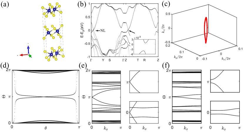
For 3D structures of Xene (X=Si, Ge, Sn, Pb), since stanene and plumbene tend to undergo dimerization when stacked into 3D structures, we only consider silicene and germanene. The -axis and -axis are equivalent in Xene, i.e., (0,1) and (1,0) are equivalent, and thus we have 3 combinations of . For each combination of , we have 3 structures, i.e., is perpendicular to both and , is inclined toward , and is inclined toward both and . The three starting structures with & are given in Fig. S21, with defined in Table. S8. We find 7 of the 9 structures, a total of 14 3D structures of Xene, with NLs. The relationship between the 9 structures is given in Table. S8. The wurtzite structure in the text corresponds to .
| (0,0) | crystal 1 (SG.194) | crystal 2 (SG.15) | crystal 3 (SG.2) |
|---|---|---|---|
| (0,1) | (SG.64) | crystal 4 (SG.15) | crystal 5 (SG.2) |
| (1,1) | (SG.64) | crystal 6 (SG.2) | crystal 7 (SG.2) |
References
- Evarestov and Smirnov [2012] R. A. Evarestov and V. P. Smirnov, Site symmetry in crystals: theory and applications, Vol. 108 (Springer Science & Business Media, 2012).
- Cano et al. [2018] J. Cano, B. Bradlyn, Z. Wang, L. Elcoro, M. G. Vergniory, C. Felser, M. I. Aroyo, and B. A. Bernevig, Building blocks of topological quantum chemistry: Elementary band representations, Phys. Rev. B 97, 035139 (2018).
- Liu et al. [2011] C.-C. Liu, H. Jiang, and Y. Yao, Low-energy effective hamiltonian involving spin-orbit coupling in silicene and two-dimensional germanium and tin, Phys. Rev. B 84, 195430 (2011).
- Kresse and Furthmüller [1996] G. Kresse and J. Furthmüller, Efficient iterative schemes for initio total-energy calculations using a plane-wave basis set, Phys. Rev. B 54, 11169 (1996).
- Mostofi et al. [2008] A. A. Mostofi, J. R. Yates, Y.-S. Lee, I. Souza, D. Vanderbilt, and N. Marzari, wannier90: A tool for obtaining maximally-localised wannier functions, Comput. Phys. Commun. 178, 685 (2008).