Optical control of multiple resistance levels in graphene for memristic applications
Abstract
Neuromorphic computing has emphasized the need for memristors with non-volatile, multiple conductance levels. This paper demonstrates the potential of hexagonal boron nitride (hBN)/graphene heterostructures to act as memristors with multiple resistance states that can be optically tuned using visible light. The number of resistance levels in graphene can be controlled by modulating doping levels, achieved by varying the electric field strength or adjusting the duration of optical illumination. Our measurements show that this photodoping of graphene results from the optical excitation of charge carriers from the nitrogen-vacancy levels of hBN to its conduction band, with these carriers then being transferred to graphene by the gate-induced electric field. We develop a quantitative model to describe our observations. Additionally, utilizing our device architecture, we propose a memristive crossbar array for vector-matrix multiplications.
I Introduction
Neuromorphic computing (NC), inspired by computing in our brain, has emerged as a new paradigm beyond von Neumann computing. NC provides a low-energy alternative to traditional von Neumann architectures, promoting sustainable computation in our modern information age. The critical hardware building blocks for NC are memristors (artificial synapse), neural processing units, and threshold switches (artificial neurons) [1, 2, 3, 4, 5]. A memristor is a fundamental electronic component where the resistance of the channel is dependent on the charge that has flown through it; it is a resistor with a memory. This charge-history dependence of resistance can be exploited in machine learning frameworks where computation can be carried out via cross-bar arrays, and synaptic weights (such as weights for neural networks) can be modified by a certain number of electrical pulses, leading to in-memory computing. A low-power, non-volatile memristor is essential to exploit NC’s benefits fully.
A prerequisite for memristic action is a platform with non-volatile doping. Chemical and electrostatic doping are the two most commonly used techniques to induce charge carriers in 2-D channels. Chemical doping is done by hetero-atom substitution and adsorption of molecular adsorbates onto graphene and other 2D materials. There are several drawbacks of this approach, including limited control over doping concentration, introduction of uncontrolled structural defects and lattice strains, unintentional impurity introduction, challenges in maintaining stability and diffusion control, and the sensitivity of the sample to processing conditions. [6, 7, 8, 9, 10, 11, 12, 13, 14].
Electrostatic doping involves doping using an external local gate. While this technique avoids most of the disadvantages of chemical doping listed above, the magnitude of doping attainable is limited by the breakdown voltage of the gate dielectric. [15, 16, 17, 18]. Liquid ionic gating has the potential of reaching higher doping levels than is achievable by dielectric gates but at the cost of device instability and non-scalability. [19, 20]
A viable alternative is optical doping of graphene on hexagonal boron nitride (hBN) substrates [21, 22, 23, 24, 25, 26, 27, 28, 29, 30, 31, 32, 33, 34, 35, 36]. hBN has a band gap of 6 eV with several intermediate defect states that can be optically excited [37, 38, 39, 40]. This method involves the controlled optical excitation of charge carriers from defect states of hBN and their transfer to graphene using an external electric field. This technique is reversible without adversely affecting transport mobility and defect density.
In this article, we present an in-depth study of optical doping in hBN/graphene heterostructures using visible light. Our research reveals that electrons in the nitrogen-vacancy defect state in hBN can be optically excited with violet light and transferred to graphene through electrostatic gating. This technique enables high-density doping of graphene, with the doping level controlled by gate voltage or illumination time. The dynamics of this doping process, measured with millisecond temporal resolution, can be adjusted over three orders of magnitude by varying the illumination wavelength and optical power. Furthermore, we demonstrate that a graphene/hBN heterostructure can function as a memristor, exhibiting multiple resistance levels. The device’s compact structure and room-temperature operation enhance its potential for scalable, room-temperature neuromorphic applications.
II Results
Single-layer graphene devices encapsulated between thin hBN crystals were fabricated using the dry transfer method (Supporting Information, section S1). 1-D electrical contacts to the graphene were achieved by lithography and dry etching, followed by Cr/Au metallization (Fig. 1(a)). A back-gate voltage, , tuned the charge carrier number density. Electrical transport measurements were performed using a low-frequency AC measurement technique. The Dirac point (maxima in the device resistance ) is attained at V (Fig. 1(b), solid blue line), attesting to the absence of charged impurities in the graphene channel.
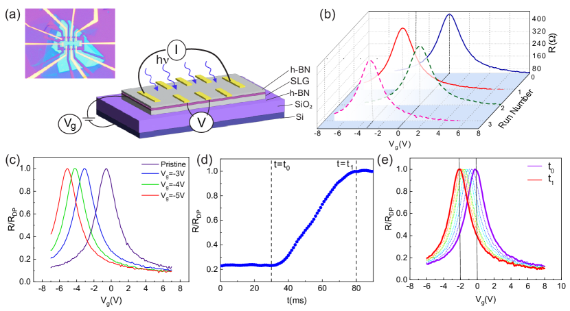
The optoelectronic measurements were carried out at room temperature, and the sample was illuminated by using either an LED of wavelength, nm or a Ti Sapphire pulsed laser (80 MHz repetition rate, fs pulse width). To photo-dope the device, we use the following protocol: The gate voltage is set to a desired value , and the device is exposed to the light of wavelength 427 nm of intensity , till the resistance saturates to the value of resistance at Dirac point. The light is then turned off, and the gate response of the device is measured. It was found that the entire plot shifts with the Dirac point at (Fig. 1(b) – solid red line; in this example V), establishing that the device is now electron-doped. We refer to this step as the ‘SET’ protocol wherein the Dirac point can be set deterministically at any desired value of (Fig. 1(c)). To ‘RESET,’ the device is exposed to a higher light intensity at V until the Dirac point shifts to V. This protocol brings the Dirac point of the device back to V (Fig. 1(b) – dotted green line). As illustrated in Fig. 1(b), the process can be repeated without degradation in the device characteristics.
Fig. 1(d) shows the time dependence of the device’s normalized longitudinal resistance during the ‘SET’ protocol with V using LED of nm and . Here, is the resistance at the Dirac point. Upon illumination, the device resistance, , increases rapidly with time, saturating in about 50 milliseconds to . Exposure for a longer duration had no discernible effect on the channel resistance. Notably, upon turning off the illumination, the device’s resistance remains unchanged.
Fig. 1(e) shows snapshots of the data in 10-second intervals. During this measurement, the light was turned on for 10 seconds with set at V. The illumination was turned off, and the curve was measured. The process is repeated multiple times to generate the plots in Fig. 1(e). The intensity of the light was kept very low (I=) to allow for a much slower rate of resistance change (for easier observations). One can see that the entire transfer curve shifts gradually to the left until the Dirac point reaches V. These measurements establish that the Dirac point can be moved deterministically to any value of the gate voltage either by controlling the exposure time (Fig.1(e)) or the value of at which the device is illuminated (Fig. 1(c)).
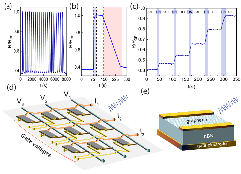
After setting up the SET/RESET protocol, we now show that the resistance of the sample at a specific gate voltage can be repeatedly alternated between two distinct values (Fig. 2(a)). The data for a single light pulse is shown in Fig. 2(b); we find that the ‘RESET’ time is significantly larger than the ‘SET’ time for electron doping. Below, we explain this observation. Moreover, adjusting the exposure time makes switching between multiple resistance values possible, as depicted in Fig. 2(c). In this measurement, the light was turned on for seconds (gray shaded region of the timeline), during which increased. The light was then turned off. The value of was stable at the value it reached when the illumination was cut off. This process can be repeated to produce multiple stable resistance levels in graphene.
III Application as memristor
As shown in Fig. 2(c), our device has at least six stable resistance states, with more resistance states also accessible by lower optical powers. Such an hBN/graphene heterostructure with multiple stable resistance values holds significant potential for developing memristor devices for vector-matrix multiplication and machine learning (ML) applications. [41, 42, 43, 44]. Several such devices can be fabricated in a cross-bar array for a typical linear algebra calculation, with voltages as inputs and currents as outputs. A new vector-matrix multiplication operation can be carried out by modifying the weights of each cross-bar intersection, i.e., by changing the resistance of the channels. For hardware implementation of ML training, the synaptic weights of a neural layer (each layer will be a separate cross-bar array) can be similarly modified.
We propose a cross-bar geometry schematically shown in Fig. 2(d) to achieve the above objectives. Its compact footprint offers distinct advantages over other structures. Each device unit (shown schematically in Fig. 2(d)) is individually gated; this architecture is easily achievable using modern nano-fabrication processes. Before each operation, the channel resistances of each device are initialized by a global incident optical beam and the application of distinct back-gate voltages to different devices. This process will ‘SET‘ the channel resistance of each device. Conversely, the ‘RESET‘ can be done by setting the desired gate voltages to zero and illuminating with a global incident optical beam.
IV Origin of the phenomenon
Photo-doping of the graphene channel requires charge transfer from hBN to graphene. The energy corresponding to violet light ( nm) is 2.9 eV, much lower than the band gap of hBN ( eV), precluding photo-excitation of carriers from the valence band of hBN. We also find that the graphene channel remained undoped in a device with only the top hBN flake and without the bottom hBN flake upon using the same protocol described above (Supporting Information, section S3). This study confirms that only the bottom hBN was responsible for the photodoping effect. Based on these observations, we sketch out a possible scenario below that explains all our experimental findings.
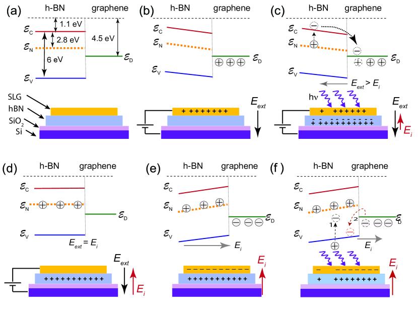
Fig. 3(a) is a schematic of the energy alignment of the bottom hBN and the graphene without photo-excitation and at . Several mid-gap states in hBN can act as electron donors. Of these, the one most relevant for us is the defect state of nitrogen vacancies (marked as in Fig. 3). This level can have stable charge states of or [38]. A negative gate-voltage dopes the graphene channel with holes and creates an electric field directed from graphene into the hBN (Fig. 3(b)) leading to band bending. Illuminating the device with violet light excites electrons from to the conduction band of hBN. These electrons are funneled to the graphene channel under the influence of the electric field. The holes left at in the hBN generate an electric field in the direction opposite (Fig. 3(c)). The electron transfer process continues until the net electric field between graphene and hBN becomes zero. Simple electrostatics arguments show that the effective number density in graphene becomes zero at this point (Fig. 3(d), which manifests as a shift of the charge neutrality point to , (Fig. 3(d)) and constitute the ’SET’ protocol.
On reducing to zero, graphene draws negative charges from the metal contacts, making the net device charge neutral (Fig. 3(e)). This charge configuration generates an electric field directed from the hBN to graphene. The consequent band bending and the fact that forbids electron transfer back from graphene to the hBN; graphene remains negatively charged, and hBN is positively charged (Fig. 3(e)). This energy barrier to back-transfer electrons from graphene to hBN explains the long-term charge retention in graphene after the photodoping is completed.
Applying a V with simultaneous exposure to light erased the doping, bringing the graphene’s Dirac point back to V. Excess electrons need to be removed from graphene and transferred back to hBN for this to happen. Note, however, that this process seems energetically unfavorable as at the interface. The physical mechanism leading to this charge-neutralization of graphene is unclear. We propose a phenomenological scenario in which this ‘RESET’ process is a two-step process involving (1) the transfer of electrons from the valence band of hBN to its mid-gap states due to optical excitation and (2) subsequent electron transfer from graphene to the empty valence band states of hBN due to electric field (Fig. 3(f)). Consequently, the ‘RESET’ process (involving electron transfer from graphene to hBN) is much slower than the ‘SET’ process for electron doping. Device-level simulations are required to verify if the above scenario correctly captures the doping erasure process.
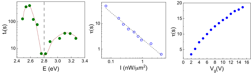
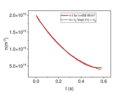
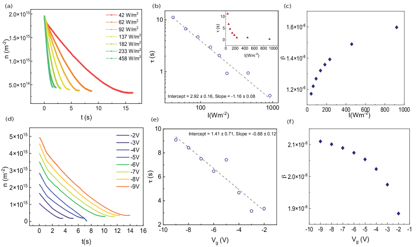
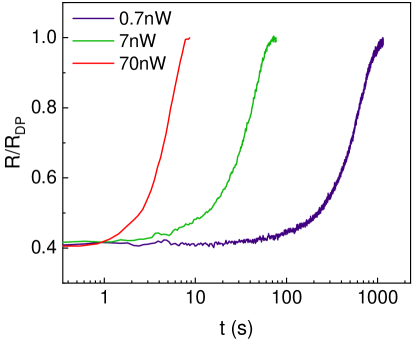
Next, we used a tunable pulse laser to study the wavelength dependence of the doping time , which we define as the time taken for the resistance to saturate to on exposure to light at a fixed . Fig. 4(a) plots versus the laser photon energy for a constant laser power nW and V. It shows a minimum in around eV. This photon energy corresponds to the optical absorption by valence nitrogen defect in hBN ‘,’ leading credence to our understanding of the photodoping process [37]. The intensity and gate-dependent measurements were done using an LED source ( nm), and the time constant was extracted by fitting number density vs. time curve to equation (S1)(Fig. S1). Intensity-dependent measurements at a fixed showed that is inversely proportional to the light intensity (Fig. 4(b)). This dependence is understandable, as an increase in the intensity of photons leads to more free charges being produced in hBN, reducing the time taken to dope (see Supplementary Information for detailed derivation). For measurements performed at a fixed intensity of light, the time constant to dope should increase with an increase in the magnitude of (equivalently, of ); measurements confirm this (Fig. 4(c)) (See Supplementary Information for a derivation).
V Conclusions
To summarize, we demonstrate a reversible control of the Dirac point in the graphene-hBN heterostructure to encode the resistance values via a combined optical-electrical stimulus. The device’s resistance can be modified by varying the gate voltage in the presence of an optical incident power or by fixing the gate voltage and illuminating it with multiple optical pulses. The switching time can be tuned by the incidence light wavelength (Fig. 4(a)), light intensity (Fig. 4(b)), or the gate voltage (Fig. 4(c)) providing tremendous tunability of the properties of the device. The time taken to electron dope is much less compared to hole doping, and further experiments need to be done to make them comparable. It should be possible to control the switching time by modifying the defect density in hBN using electron irradiation or annealing processes. The ability to photoelectrically ‘SET,’ ‘READ,’ and ‘RESET’ multiple stable and non-volatile resistance states of the device makes it ideal for use as a memristor.
Methods
Device Fabrication
The devices were fabricated using the dry transfer technique [45]. Single-layer graphene (SLG) and hexagonal boron nitride (hBN) flakes were mechanically exfoliated onto a \chSi/\chSiO2 substrates. The hBN flakes had a thickness of 25-30 nm. Electron beam lithography was used to define electrical contacts. This was followed by etching with a mixture of (40 sscm) and (10 sscm). The metallization was done with Cr/Au (5 nm/60 nm) to form the 1D electrical contacts with SLG.
Measurements
All electrical transport measurements were performed at room temperature using a low-frequency AC measurement technique. For low-temperature measurements, the sample was cooled down in a cryostat to 4.7 K. For optoelectronic measurements, the sample was illuminated using either an LED of wavelength, nm, or a Ti Sapphire pulsed laser (80 MHz repetition rate, fs pulse width).
Acknowledgement
A.B. acknowledges funding from the Department of Science & Technology FIST program and the U.S. Army DEVCOM Indo-Pacific (Project number: FA5209 22P0166). K.W. and T.T. acknowledge support from JSPS KAKENHI (Grant Numbers 19H05790, 20H00354, and 21H05233). A.S. acknowledges funding from Indian Institute of Science start-up grant, DST Nanomission CONCEPT (Consortium for Collective and Engineered Phenomena in Topology) grant and project MoE-STARS-2/2023-0265. M.M. acknowledges Prime Minister’s Research Fellowship (PMRF).
Data availability
The authors declare that the data supporting the findings of this study are available within the main text and its supplementary Information. Other relevant data are available from the corresponding author upon reasonable request.
Author Contributions
H.K.M, M.M., V.S., A.S., and A.B. conceptualized the study, performed the measurements, and analyzed the data. K.W. and T.T. grew the hBN single crystals. All the authors contributed to preparing the manuscript.
Competing interests:
The authors declare no Competing Financial or Non-Financial Interests.
Supporting Information
Supporting information contains detailed discussions of the (S1) device fabrication, (S2)dependence of on and , (S3) top or bottom hBN responsible for doping, (S4) doping at low temperatures and (S5) minimum detectable power.
Supplementary Materials
S1 Device Fabrication
The devices were fabricated using the dry transfer technique [45]. Single-layer graphene (SLG) and hexagonal boron nitride (hBN) flakes were mechanically exfoliated onto a \chSi/\chSiO2 substrates. The hBN flakes had a thickness of 25-30 nm. The SLG flakes were identified from optical contrast under a microscope and later confirmed with Raman spectra. Electron beam lithography was used to define electrical contacts. This was followed by etching with a mixture of (40 sscm) and (10 sscm). The metallization was done with Cr/Au (5 nm/60 nm) to form the 1D electrical contacts with SLG.
S2 Dependence of on and
As discussed in the main manuscript, illuminating the device with the gate voltage held at a gate voltage leads to the shift of the Dirac point to . Consider the graphene channel with the gate voltage set to before turning the light on. The channel is hole-doped to a value . Here, is the capacitance of the bottom hBN layer.
On turning on the light, the hole density decreases exponentially with time with a time constant (Fig. S1):
| (S1) |
where is the residual charge density at the Dirac point. From Eqn. S1, we get:
| (S2) |
It follows that the areal number density of electrons excited in time from the N-vacancy mid-gap state to the conduction band of hBN is:
| (S3) |
Here is the number of photons incident on the device per unit area per unit time, is the efficiency of the electron excitation process in hBN. For simplicity, we assume that all the electrons produced in hBN are instantly swept to graphene by the process explained in the main manuscript. Combining Eqn. S2 and Eqn. S3, we get
For ,this reduces to
or,
| (S4) |
Eqn. (S4) implies that the time constant for doping should be directly proportional to and inversely proportional to . Below, we probe the and dependence of . We also get the values of .
Intensity dependence:
For these measurements, the gate voltage is kept constant at V, and data are collected for different values of . Some representative plots are shown in Fig. S2(a). The data are fitted using Eqn. (S1) to extract the values of , and . Fig. S2(b) is the plot of versus . A double log fit yields establishing to be inversely proportional to and matching the prediction of Eqn. (S4). From the fit, we get in the range , the data are plotted in Fig. S2(c).
Gate Voltage dependence:
For this set of measurements, the light intensity is kept fixed at . Data are collected for different values of (Fig. S2(d)). The data are fitted using Eqn. (S1) to extract the values of (Fig. S2(e)). The dotted line is a linear fit to the data. The excellent fit establishes that , matching the prediction of Eqn. (S4). The slope of the curve () yields to lie in the range of (Fig. S2(f)).
S3 Top or bottom hBN responsible for doping
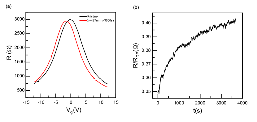
In our heterostructure, there are two hBN flakes, one at the top and one at the bottom of the graphene. The discussion in the main manuscript assumes that the top hBN does not play any role in the doping process; note that all measurements reported in this work were performed with the back gate bias. To confirm this, we fabricated a device with only top hBN and illuminated it with the light of nm at a back-gate voltage of V. As shown in Fig. S3, the shift in Dirac point, even after prolonged exposure of one hour with high-intensity light, is very small, significantly less than the doping effect observed in our original device, which was V in 50 ms. Hence, the contribution from the top hBN is negligible, and the bottom hBN is responsible for the doping effect.
S4 Doping at low temperatures
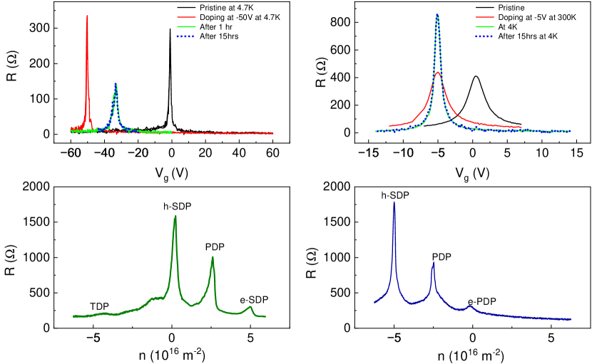
Quantum transport measurements are performed at low temperatures. We tested the compatibility of our doping process with low-temperature measurements. The sample was doped at room temperature for the low-temperature experiments and then cooled down in a cryostat. As shown in Fig. S4(a), doping was retained at low temperatures, and the response of the sample remained unchanged even after hours when kept cool. By contrast, when the doping was done at lower temperatures, we found the device did not retain the doping, as shown in Fig. S4(b). Hence, the doping should be done at room temperature, and then the device can be cooled down.
An important application of the photodoping process discussed in this work is in accessing high-energy regions of the bands in graphene, which can not be reached by traditional electrostatic doping. Using this method, we doped an hBN/SLG moiré device to electron and hole number densities of as shown in Fig. S4(c,d). We can access the tertiary Dirac point () on the hole side; this was inaccessible in previous measurements due to gate-leakage during standard electrostatic gating.
S5 Minimum detectable power
The device was illuminated with different powers of light of nm at negative gate voltage V, and the corresponding resistance versus time curves were recorded as shown in figure Fig. S5. The illumination power () was measured using a power meter. We could observe a change in the resistance for as low as nW.
References
- Sangwan and Hersam [2020] V. K. Sangwan and M. C. Hersam, Neuromorphic nanoelectronic materials, Nature Nanotechnology 15, 517 (2020).
- Walters et al. [2023] B. Walters, M. V. Jacob, A. Amirsoleimani, and M. Rahimi Azghadi, A Review of Graphene-Based Memristive Neuromorphic Devices and Circuits, Advanced Intelligent Systems 5, 2300136 (2023).
- Lu et al. [2014] H. Lu, A. Lipatov, S. Ryu, D. J. Kim, H. Lee, M. Y. Zhuravlev, C. B. Eom, E. Y. Tsymbal, A. Sinitskii, and A. Gruverman, Ferroelectric tunnel junctions with graphene electrodes, Nature Communications 5, 5518 (2014).
- Wu et al. [2020] J. Wu, H.-Y. Chen, N. Yang, J. Cao, X. Yan, F. Liu, Q. Sun, X. Ling, J. Guo, and H. Wang, High tunnelling electroresistance in a ferroelectric van der Waals heterojunction via giant barrier height modulation, Nature Electronics 3, 466 (2020).
- Yan et al. [2023] X. Yan, Z. Zheng, V. K. Sangwan, J. H. Qian, X. Wang, S. E. Liu, K. Watanabe, T. Taniguchi, S.-Y. Xu, P. Jarillo-Herrero, Q. Ma, and M. C. Hersam, Moiré synaptic transistor with room-temperature neuromorphic functionality, Nature 624, 551 (2023).
- Liu et al. [2011] H. Liu, Y. Liu, and D. Zhu, Chemical doping of graphene, Journal of Materials Chemistry 21, 3335 (2011).
- Wehling et al. [2008] T. O. Wehling, K. S. Novoselov, S. V. Morozov, E. E. Vdovin, M. I. Katsnelson, A. K. Geim, and A. I. Lichtenstein, Molecular Doping of Graphene, Nano Letters 8, 173 (2008).
- Jung et al. [2009] N. Jung, N. Kim, S. Jockusch, N. J. Turro, P. Kim, and L. Brus, Charge Transfer Chemical Doping of Few Layer Graphenes: Charge Distribution and Band Gap Formation, Nano Letters 9, 4133 (2009).
- Bruna and Borini [2010] M. Bruna and S. Borini, Observation of Raman $G$-band splitting in top-doped few-layer graphene, Physical Review B 81, 125421 (2010).
- Zhan et al. [2010] D. Zhan, L. Sun, Z. H. Ni, L. Liu, X. F. Fan, Y. Wang, T. Yu, Y. M. Lam, W. Huang, and Z. X. Shen, FeCl3-Based Few-Layer Graphene Intercalation Compounds: Single Linear Dispersion Electronic Band Structure and Strong Charge Transfer Doping, Advanced Functional Materials 20, 3504 (2010).
- Zhao et al. [2011] W. Zhao, P. H. Tan, J. Liu, and A. C. Ferrari, Intercalation of Few-Layer Graphite Flakes with FeCl3: Raman Determination of Fermi Level, Layer by Layer Decoupling, and Stability, Journal of the American Chemical Society 133, 5941 (2011).
- Zhao et al. [2010] W. Zhao, P. Tan, J. Zhang, and J. Liu, Charge transfer and optical phonon mixing in few-layer graphene chemically doped with sulfuric acid, Physical Review B 82, 245423 (2010).
- Singh et al. [2012] A. K. Singh, M. W. Iqbal, V. K. Singh, M. Z. Iqbal, J. H. Lee, S.-H. Chun, K. Shin, and J. Eom, Molecular n-doping of chemical vapor deposition grown graphene, Journal of Materials Chemistry 22, 15168 (2012).
- Medina et al. [2011] H. Medina, Y.-C. Lin, D. Obergfell, and P.-W. Chiu, Tuning of Charge Densities in Graphene by Molecule Doping, Advanced Functional Materials 21, 2687 (2011).
- Ryu et al. [2010] S. Ryu, L. Liu, S. Berciaud, Y.-J. Yu, H. Liu, P. Kim, G. W. Flynn, and L. E. Brus, Atmospheric Oxygen Binding and Hole Doping in Deformed Graphene on a SiO2 Substrate, Nano Letters 10, 4944 (2010).
- Dean et al. [2010] C. R. Dean, A. F. Young, I. Meric, C. Lee, L. Wang, S. Sorgenfrei, K. Watanabe, T. Taniguchi, P. Kim, K. L. Shepard, and J. Hone, Boron nitride substrates for high-quality graphene electronics, Nature Nanotechnology 5, 722 (2010).
- Das et al. [2008] A. Das, S. Pisana, B. Chakraborty, S. Piscanec, S. K. Saha, U. V. Waghmare, K. S. Novoselov, H. R. Krishnamurthy, A. K. Geim, A. C. Ferrari, and A. K. Sood, Monitoring dopants by Raman scattering in an electrochemically top-gated graphene transistor, Nature Nanotechnology 3, 210 (2008).
- Yan et al. [2007] J. Yan, Y. Zhang, P. Kim, and A. Pinczuk, Electric Field Effect Tuning of Electron-Phonon Coupling in Graphene, Physical Review Letters 98, 166802 (2007).
- Chen et al. [2009] F. Chen, Q. Qing, J. Xia, J. Li, and N. Tao, Electrochemical Gate-Controlled Charge Transport in Graphene in Ionic Liquid and Aqueous Solution, Journal of the American Chemical Society 131, 9908 (2009).
- Uesugi et al. [2013] E. Uesugi, H. Goto, R. Eguchi, A. Fujiwara, and Y. Kubozono, Electric double-layer capacitance between an ionic liquid and few-layer graphene, Scientific Reports 3, 1595 (2013).
- Tiberj et al. [2013] A. Tiberj, M. Rubio-Roy, M. Paillet, J. R. Huntzinger, P. Landois, M. Mikolasek, S. Contreras, J. L. Sauvajol, E. Dujardin, and A. A. Zahab, Reversible optical doping of graphene, Scientific Reports 3, 2355 (2013).
- Aftab et al. [2022] S. Aftab, M. Z. Iqbal, and M. W. Iqbal, Programmable Photo-Induced Doping in 2D Materials, Advanced Materials Interfaces 9, 2201219 (2022).
- Neumann et al. [2016] C. Neumann, L. Rizzi, S. Reichardt, B. Terrés, T. Khodkov, K. Watanabe, T. Taniguchi, B. Beschoten, and C. Stampfer, Spatial control of laser-induced doping profiles in graphene on hexagonal boron nitride, ACS Applied Materials & Interfaces 8, 9377 (2016).
- Ju et al. [2014] L. Ju, J. V. Jr, E. Huang, S. Kahn, C. Nosiglia, H.-Z. Tsai, W. Yang, T. Taniguchi, K. Watanabe, Y. Zhang, G. Zhang, M. Crommie, A. Zettl, and F. Wang, Photoinduced doping in heterostructures of graphene and boron nitride, Nature Nanotechnology 9, 348 (2014).
- Roy et al. [2013] K. Roy, M. Padmanabhan, S. Goswami, T. P. Sai, G. Ramalingam, S. Raghavan, and A. Ghosh, Graphene–MoS2 hybrid structures for multifunctional photoresponsive memory devices, Nature Nanotechnology 8, 826 (2013).
- Kim et al. [2013] Y. D. Kim, M.-H. Bae, J.-T. Seo, Y. S. Kim, H. Kim, J. H. Lee, J. R. Ahn, S. W. Lee, S.-H. Chun, and Y. D. Park, Focused-laser-enabled p–n junctions in graphene field-effect transistors, ACS Nano 7, 5850 (2013).
- Song et al. [2021] S.-B. Song, S. Yoon, S. Y. Kim, S. Yang, S.-Y. Seo, S. Cha, H.-W. Jeong, K. Watanabe, T. Taniguchi, G.-H. Lee, J. S. Kim, M.-H. Jo, and J. Kim, Deep-ultraviolet electroluminescence and photocurrent generation in graphene/hBN/graphene heterostructures, Nature Communications 12, 7134 (2021).
- Velasco et al. [2016] J. J. Velasco, L. Ju, D. Wong, S. Kahn, J. Lee, H.-Z. Tsai, C. Germany, S. Wickenburg, J. Lu, T. Taniguchi, K. Watanabe, A. Zettl, F. Wang, and M. F. Crommie, Nanoscale control of rewriteable doping patterns in pristine graphene/boron nitride heterostructures, Nano Letters 16, 1620 (2016).
- Kim et al. [2019] S. H. Kim, S.-G. Yi, M. U. Park, C. Lee, M. Kim, and K.-H. Yoo, Multilevel MoS Optical Memory with Photoresponsive Top Floating Gates, ACS Applied Materials & Interfaces 11, 25306 (2019).
- Liu et al. [2014] C.-H. Liu, Y.-C. Chang, T. B. Norris, and Z. Zhong, Graphene photodetectors with ultra-broadband and high responsivity at room temperature, Nature Nanotechnology 9, 273 (2014).
- Xiang et al. [2018] D. Xiang, T. Liu, J. Xu, J. Y. Tan, Z. Hu, B. Lei, Y. Zheng, J. Wu, A. H. C. Neto, L. Liu, and W. Chen, Two-dimensional multibit optoelectronic memory with broadband spectrum distinction, Nature Communications 9, 2966 (2018).
- Tran et al. [2019] M. D. Tran, H. Kim, J. S. Kim, M. H. Doan, T. K. Chau, Q. A. Vu, J.-H. Kim, and Y. H. Lee, Two-Terminal Multibit Optical Memory via van der Waals Heterostructure, Advanced Materials 31, 1807075 (2019).
- Lee et al. [2020] I. Lee, W. T. Kang, J. E. Kim, Y. R. Kim, U. Y. Won, Y. H. Lee, and W. J. Yu, Photoinduced Tuning of Schottky Barrier Height in Graphene/MoS2 Heterojunction for Ultrahigh Performance Short Channel Phototransistor, ACS Nano 14, 7574 (2020).
- Gorecki et al. [2018] J. Gorecki, V. Apostolopoulos, J.-Y. Ou, S. Mailis, and N. Papasimakis, Optical Gating of Graphene on Photoconductive Fe:LiNbO3, ACS Nano 12, 5940 (2018).
- Seo et al. [2014] B. H. Seo, J. Youn, and M. Shim, Direct Laser Writing of Air-Stable p–n Junctions in Graphene, ACS Nano 8, 8831 (2014).
- Miller et al. [2020] D. Miller, A. Blaikie, and B. J. Alemán, Nonvolatile Rewritable Frequency Tuning of a Nanoelectromechanical Resonator Using Photoinduced Doping, Nano Letters 20, 2378 (2020).
- Attaccalite et al. [2011] C. Attaccalite, M. Bockstedte, A. Marini, A. Rubio, and L. Wirtz, Coupling of excitons and defect states in boron-nitride nanostructures, Physical Review B 83, 144115 (2011).
- Weston et al. [2018] L. Weston, D. Wickramaratne, M. Mackoit, A. Alkauskas, and C. G. Van De Walle, Native point defects and impurities in hexagonal boron nitride, Physical Review B 97, 214104 (2018).
- Sajid et al. [2018] A. Sajid, J. R. Reimers, and M. J. Ford, Defect states in hexagonal boron nitride: Assignments of observed properties and prediction of properties relevant to quantum computation, Phys. Rev. B 97, 064101 (2018).
- Strand et al. [2020] J. Strand, L. Larcher, and A. L. Shluger, Properties of intrinsic point defects and dimers in hexagonal boron nitride, Journal of Physics: Condensed Matter 32, 055706 (2020).
- Ducry et al. [2022] F. Ducry, D. Waldhoer, T. Knobloch, M. Csontos, N. Jimenez Olalla, J. Leuthold, T. Grasser, and M. Luisier, An ab initio study on resistance switching in hexagonal boron nitride, npj 2D Materials and Applications 6, 1 (2022).
- Xie et al. [2022] J. Xie, S. Afshari, and I. Sanchez Esqueda, Hexagonal boron nitride (h-BN) memristor arrays for analog-based machine learning hardware, npj 2D Materials and Applications 6, 1 (2022).
- Maier et al. [2016] P. Maier, F. Hartmann, M. Emmerling, C. Schneider, M. Kamp, S. Höfling, and L. Worschech, Electro-Photo-Sensitive Memristor for Neuromorphic and Arithmetic Computing, Physical Review Applied 5, 054011 (2016).
- Schranghamer et al. [2020] T. F. Schranghamer, A. Oberoi, and S. Das, Graphene memristive synapses for high precision neuromorphic computing, Nature Communications 11, 5474 (2020).
- Tiwari et al. [2023] P. Tiwari, D. Sahani, A. Chakraborty, K. Das, K. Watanabe, T. Taniguchi, A. Agarwal, and A. Bid, Observation of the Time-Reversal Symmetric Hall Effect in Graphene–WSe2 Heterostructures at Room Temperature, Nano Letters 23, 6792 (2023).