Ab-initio transport properties of nanostructures from maximally-localized Wannier functions
Abstract
We present a comprehensive first-principles study of the ballistic transport properties of low dimensional nanostructures such as linear chains of atoms (Al, C) and carbon nanotubes in presence of defects. A novel approach is introduced where quantum conductance is computed from the combination of accurate plane-wave electronic structure calculations, the evaluation of the corresponding maximally-localized Wannier functions, and the calculation of transport properties by a real-space Green’s function method based on the Landauer formalism. This approach is computationally very efficient, can be straightforwardly implemented as a post-processing step in a standard electronic-structure calculation, and allows to directly link the electronic transport properties of a device to the nature of the chemical bonds, providing insight onto the mechanisms that govern electron flow at the nanoscale.
pacs:
71.15.Ap,72.10.-d,73.63.-bI Introduction
The field of nanotechnology has undergone a remarkable growth in the last few years. This development has been fueled by the expectation that unusual properties of matter, nygard ; park ; liang which become evident as the dimensions of the structural components of a device shrink under 10-100 nm, may be exploited. Indeed, the challenges for future developments involve continuous shrinking of the physical dimensions of devices and attainment of higher speeds. The drive to produce smaller devices has led the current research towards new forms of electronics, in which nanoscale objects and molecular devices replace the transistors of today’s silicon technology. aviram ; joachim ; williams ; gudiksen Experiments have been performed to directly measure charge transport properties of hybrid metal-(bio)molecular systems aviram ; joachim ; reed ; collier ; metzger ; braun ; reichert ; smit ; lahann and carbon-based aggregates such as fullerenes and nanotubes. williams ; nygard ; tans ; white ; ouyang ; collins Particular attention has been devoted to atomic-scale devices, since they represent the limit towards one-dimensional electronics, and thus the transport properties of wire-like chains of atoms (especially Au, Al and C), connected with metal electrodes have been widely investigated. agrait ; ohnishi ; yanson ; nilius Despite their simple structures, atomic-sized chains display peculiar quantum properties due to their low dimensionality; in particular, the electronic properties are strongly affected by the nature of single chemical bonds and coordination numbers.
The ongoing rapid advances in the measurements of electrical conductance in individual molecular- and atomic-sized devices require commensurate advances in the theoretical understanding of the detailed microscopic mechanisms that control charge mobility. Modeling of single nano-elements and coupled arrays of nano-devices is needed to provide interpretation and feedback to experimental measurements, to predict device characteristics, and to provide a basis for the functional progress of these new devices.
In general, the electron transport properties of nanostructures can be simply described in the Landauer formalism. landauer ; datta The Landauer relation connects the quantum conductance with the transmission function : its evaluation requires the knowledge of the electronic structure of the system under consideration and the inclusion of scattering at contacts. This approach relies on the evaluation of lattice Green’s functions of the system. Several approaches have been developed to calculate the quantum conductance in nanostructures, based on semi-empirical (tight-binding, Hückel) models marco ; todorov ; kristic ; rego ; more recently, a variety of first-principles formulations have appeared. lang1 ; choi ; landman ; landman1 ; yoon ; guo ; yaliraki ; stokbro ; palacios ; datta1 Ab-initio approaches have also been extensively used to characterize the electrical properties of nano- and bio-materials, arrigo ; parrinello1 and to study the effects of microscopic structural relaxation and of electrode/conductor junctions. rosa
In this paper, we present an original approach to the calculation of coherent transport properties of nanostructures from first principles. Our methodology combines an accurate description of the electronic ground state provided by well-developed first-principles calculations based on plane-wave (PW) representations, with the Landauer approach to describe transport properties of extended systems. marco1 ; marco2 The essential connection is provided by the use of the maximally-localized Wannier function representation nicola that allows to introduce naturally the ground-state electronic structure into the lattice Green’s function approach that will be our basis for the evaluation of the Landauer quantum conductance.
The paper is organized as follows. In Section II we describe the main features of the method. In Section III we will study the bulk electronic and conduction properties of linear chains of Al and C atoms. Section IV deals with the conduction properties of a carbon nanotube with a substitutional defect. This example is used to elaborate on the formulation of the two-terminal conductance problem in our approach. The paper ends with Section V where our conclusions are presented.
II Method
II.1 Electronic transport in extended systems
Calculations of the quantum conductance are based on a recently developed efficient method for evaluating quantum transport in extended systems. marco ; marco1 ; marco2 This method is applicable to any Hamiltonian that can be expanded within a localized-orbital basis and can be used as a general theoretical scheme for the computation and analysis of the electrical properties of nanostructures.
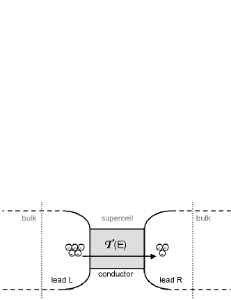
Let us consider a system composed of a conductor
connected to two semi-infinite leads, as in Fig. 1. The
quantum description of the electronic conductance is a complex
non-equilibrium problem. We begin the study of conduction properties
focusing on the coherent electron transport. This approach
leaves out non-equilibrium effects due, e.g., to dissipative
scattering or to an external bias.
Quantum conductance () is the microscopic quantity that characterizes the transport properties of a conductor and may be calculated using the Landauer expression: landauer
| (1) |
where (E) is the transmission function, i.e. the probability that an electron injected at one end of the conductor with energy E will be transmitted to the other end. In the Green’s function formalism the transmission function is expressed as datta
| (2) |
where are the retarded and advanced Green’s functions of the conductor, and represent the coupling of the conductor to the leads.
The effect of the semi-infinite leads on the conductor can be described by means of finite-dimension operators known as the self-energies . The Green’s function and the coupling functions of Eq. 2 are explicitly obtained from the self-energies as:
| (3) |
| (4) |
where is the Hamiltonian matrix of the conductor, calculated with respect to a localized real-space basis set; in our approach all these operators will be represented in the basis set of the maximally-localized ground-state Wannier functions (WFs) for the system examined. This will allow a mapping for the first-principles Hamiltonian onto an exact band-structure tight-binding model, for which we then follow the detailed Landauer formulation of Ref. marco, .
The key assumption is the description of the original system as a sequence of principal layers, lee along which we calculate the transport properties and where the interaction between adjacent layers is accounted for by transfer matrices and . Within this approach the self-energies due to the semi-infinite leads are marco
| (5) |
where , are the coupling matrices for the conductor-lead assembly, and are the matrix elements of the Hamiltonian for the infinite (bulk-like) leads. For instance, describes the intralayer interactions and the interlayer coupling between two adjacent layers. If the orbitals are sufficiently localized, the residual coupling with layers farther apart will be negligible; conversely, the localization properties of the orbitals spanning the desired energy window determine the minimal thickness for a principal layer. The transfer matrices and are also computed from the Hamiltonian matrix elements via an iterative procedure. garcia
The only required inputs then are the matrix elements of the Hamiltonian expanded in a localized-orbital basis; by choosing the maximally-localized WFs representation, we provide essentially an exact mapping of the ground state onto a minimal basis. note_metal The accuracy of the results directly depends on having principal layers that do not couple beyond next-neighbors, i.e. on having a well-localized basis.
II.2 Ab-initio electronic structure
The starting point for our procedure is the first-principles calculation of the electronic structure of the nanostructure, eventually coupled to the leads. We adopt a standard electronic-structure method based on self-consistent total energy and force minimization, which allows to optimize simultaneously the atomic positions and the corresponding electronic wavefunctions. The electronic structure is described within Density Functional Theory (DFT). dreizler The examples presented in the following Section are obtained in the Local Density Approximations (LDA), pederw but more sophisticated corrections at the exchange-correlation functional (e.g. generalized gradient approximation) can obviously be used. The electron-ion interaction is described via norm-conserving pseudopotentials tm in the form of Kleinman and Bylander. kb We use Periodic Boundary Conditions (PBC) along the three directions of direct space and the electronic wavefunctions are expanded in a plane-wave basis set compatible with the chosen PBC. While the translational invariance makes the plane waves a very natural choice to describe the wavefunctions of a periodic system, the drawback is that they are truly delocalized. Brillouin Zone (BZ) summation are performed with homogeneous Monkhorst-Pack grids mp of k-points in the the first Brillouin Zone.
This approach to electronic-structure calculations is widely used, provides a faithful description of the electronic properties of the systems of interest, and in the present context it has been successfully applied to the investigation of both solid-state and molecular assemblies. jones ; wimmer The results of such calculations are, at each k-point, the Kohn-Sham energy eigenvalues and their corresponding eigenvectors (Bloch states), expanded in plane waves. It is worth noting that the present methodology to compute quantum transport from first-principles will apply to any electronic-structure approach, since it can construct and employ orbitals that are maximally-localized, and that represent a minimal basis set, under the single assumption that eigenstates are in the Bloch form. Even if the basis set used is already localized (albeit not minimal) the localization procedure will allow to recover exact results with smaller systems. In particular, our procedure can be applied in combination with Car-Parrinello molecular dynamics simulations, opening the way to compute quantum conductance in large-scale systems, and as a function of temperature, completely from first-principles.LeeMBNMarzari
II.3 Maximally-localized WFs
Bloch orbitals cannot be used directly to evaluate electronic transport with the method outlined in Sec. II.1. As we have pointed out, the quantum conductance is computed starting from the knowledge of the lattice Green’s function, whose calculation relies on a localized orbital representation of the electronic states in real space. Bloch orbitals, that are intrinsically delocalized, have to be transformed into localized functions in order to construct the sparse, short-ranged matrix elements of the Hamiltonian. The core of our proposed methodology is to use maximally-localized WFs for the system considered. These are the most natural choice for a set of localized orbitals that still span the same Hilbert space of the Hamiltonian eigenfunctions, and they allow to bridge plane-wave electronic structure and lattice Green’s function calculations in a coherent fashion. In the case of an isolated system the maximally-localized WFs become Boys localized orbitals; boys therefore, our procedure is not tied to an extended-systems formulation, but can equally well represent isolated molecules. (In addition, the localization procedure is greatly simplified for the case of large unit cells, when -sampling only is used Silvestrelli ).
A Wannier function , labeled by the Bravais lattice vector R, is usually defined via a unitary transformation of the Bloch functions of the th band:
| (6) |
where V is the volume of the unit cell and the integration is performed over the entire Brillouin Zone. It is easy to show that the WFs defined as above form an orthonormal basis set, and that any two of them, for a given index and different and , are just translational images of each other. Note that, as the WFs form a (continuous) linear combinations of Bloch functions with different energies, they do not represent stationary states, but still span exactly the same original Hilbert space. The ab-initio eigenstates are well-defined, modulus an arbitrary -dependent phase factor; thus, the definition above does not lead to a unique set of Wannier functions kohn , since the electronic structure problem is invariant for the transformation . Besides this freedom in the choice of phases for the Bloch functions, there is a more comprehensive gauge freedom stemming from the fact that the many-body wavefunction is actually a Slater determinant: a unitary transformation between orbitals will not change the manifold, and will not change the total energy and the charge density of the system. In all generality, starting with a set of Bloch functions with periodic parts , we can constructs infinite sets of WFs displaying different spatial characteristics:
| (7) |
The unitary matrices include also the gauge freedom on phase factors afore mentioned. nicola
For our purposes, we need to transform the Bloch eigenstates in WFs with the narrowest spatial distribution. We construct maximally-localized WFs using the algorithm proposed by Marzari and Vanderbilt. nicola We define a Spread Operator () as the sum of the second moments of the Wannier functions corresponding to one choice of translational lattice vector:
| (8) |
where the sum is over the group of bands which spans the Hilbert space. The value of the spread depends on the choice of unitary matrices ; thus it is possible to evolve any arbitrary set of until the minimum condition
| (9) |
is satisfied. At the minimum, we obtain the matrices that transform the first-principles into the maximally-localized WFs :
| (10) |
A useful feature of the method is that the only ingredients needed to calculate the spread functional and to evolve the unitary matrices are the overlap matrix between the periodic part of the Bloch states at neighboring k-points:
| (11) |
where b is the vector that links neighboring k-points in the discretized BZ integrals. note_ref
It is important to notice that whenever a Born-von Karman discretization
of the Brillouin Zone is introduced, even the above-mentioned WFs are not truly
localized, but will be periodic in real-space, with a superperiodicity
determined by the BZ discretization. The truly isolated limit is
recovered only in the case of continuous BZ integrations.
This is easily seen remembering that
, and has the
periodicity of the direct lattice; thus the phase factors
determine the
superperiodicity of the themselves.
In the standard language of electronic-structure
calculations, if the have ’s that are restricted to
a uniform Monkhorst-Pack mesh, they will all be periodic with a wavelength
inversely proportional to the spacing of the mesh; this periodicity is
consequently inherited by the WFs.
For k-points along a
direction of the BZ, the WFs will repeat along the corresponding
direction every cells;
therefore a mesh of k-points needs to be dense enough to assure
that adjacent replicas of the WFs do not overlap.
The method described above works properly in the case of isolated groups of bands. note1 On the other hand to study quantum conductance in extended systems we often need to compute WFs for a subset of energy bands that are entangled or mixed with other bands. Most often we are interested in the states that lie in the vicinity of the Fermi level of a conductor in a restricted energy range. Since the unitary transformations mix energy bands at each k-point, any arbitrary choice of states inside a prescribed window will affect the localization properties of WFs unless energy gaps effectively separate the manifold of interest from higher and lower bands. This problem has been solved by Souza, Marzari, and Vanderbilt, introducing an additional disentanglement procedure ivo2 that automatically extracts the best possible manifold of a given dimension from the states falling in a predefined energy window. This is the generalization to entangled or metallic cases of the maximally-localized WF formulation. The procedure relies on minimizing the subspace dispersion across the Brillouin Zone, and effectively extracts the bands of interest from the overall band structure. In practice, first we select a desired number of bands in an energy window; then we determine the optimally-connected subspace that can be extracted from that band structure; and finally we proceed with a standard localization procedure inside the selected subspace, using the same kind of spread functional and of unitary matrices . The resulting orbitals have the same good localization properties, and allow to apply our formalism to arbitrary systems, independently of the insulating or metallic nature of the band manifold. It should be stressed that the WFs obtained in the later case are not the WFs of the occupied subspace (that would exhibit poor localization properties), but are those of a well connected, continuous subspace that in general will contain both occupied and unoccupied Bloch functions.
In order to calculate the conductance according to the prescriptions outlined in Sec. II.1, we need as an input the matrix elements of the Hamiltonian calculated on a localized basis: in our case, it is the minimal basis of the maximally-localized WFs. The advantages of this choice are twofold: firstly, besides being a minimal basis, the WFs span exactly the Hilbert space of an insulator and, with arbitrary accuracy, of an entangled metallic system. Secondly, their localization assures the choice of the system with the smallest number of atomic layers. The Hamiltonian matrices (, , , ) can be formally obtained from the on site () and coupling () matrices between principal layers. In our formalism, and assuming a BZ sampling fine enough to eliminate the interaction with the periodic images, we can simply compute these matrices from the unitary matrix obtained in the localization procedure. note2 By definition of energy eigenvalues (), the Hamiltonian matrix , is diagonal in the basis of the Bloch eigenstates. We can calculate the Hamiltonian matrix in the rotated basis,
| (12) |
Next we Fourier transform into a set of Bravais lattice vectors R within a Wigner-Seitz supercell centered around R=0 :
| (13) |
where derives from the folding of the uniform mesh of k-points in the BZ. The term with R=0 provides the on site matrix , and the term R=1 provides the coupling matrix : These are the only ingredients required for the evaluation of the quantum conductance.
III Bulk-like conductance
As a first application of our method, we consider a case in which leads and conductor (as sketched in Fig. 1) are made of the same material, and we compute the conductance of the ideal and infinite nanostructure (bulk-like conductance). In this case, it is not necessary to distinguish between conductor and lead terms and the single layer and the coupling matrices are the only necessary input.
We will focus on one-dimensional (1D) linear chains of atoms. The systems that have been studied most are chains of Au, ohnishi ; yanson ; nilius ; todorov ; portal ; bahn ; mehrez , Al sen ; zheng and C. ravagnan ; lang ; larade ; abdurahman In the following, we will discuss results for Al (Sec. III.1) and C (Sec. III.2) chains.
III.1 Aluminum chain
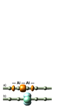
An ideal and infinite Al chain is simulated using periodic boundary conditions and a unit cell containing two aluminum atoms. A large vacuum region ( Å) in the direction perpendicular to the chain prevents the interaction with adjacent replicas. A () grid of k-points and 18 Ry energy cut-off for the wavefunction expansion assure the convergence of the electronic structure of the system. The optimized Al-Al distance ( Å) is in very good agreement with previous DFT investigations. sen ; zheng
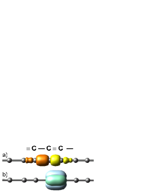
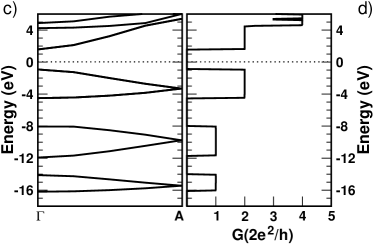
Following the procedure described above, we calculated the electronic structure and quantum conductance of this system. To construct the WFs we selected an energy window with E eV around the Fermi level (taken as the reference zero). This energy window contains all the occupied bands and the first empty states. We chose to extract an 8-dimensional manifold from this energy window: After the disentanglement and localization procedure, we obtain eight WFs which span the 8-dimensional Hilbert manifold and represent an orthonormal minimal basis for it. Thus, the calculation of quantum conductance involves operations with very small () matrices, with a negligible computational effort, exactly comparable to a tight-binding calculation (TB) with two sites and four orbital per site. However, our results provide more information on the electronic structure than the TB approach. The calculated WFs (Fig. 2a,b) are well characterized and are consistent with the estimated chemical bonds present in the system ( and orbitals). The states are centered in the middle of the Al-Al bond, while the states are localized around single atoms.
As a test of the accuracy of the WF transformation, we have computed back the band structure of the Al-chain, starting from the Wannier-function Hamiltonian in real space. This Hamiltonian can now be Fourier transformed in reciprocal space (Eq. 13) for any arbitrary k-point
| (14) |
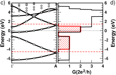
the resulting Hamiltonian matrices can then be diagonalized to find energy eigenvalues. Comparing the original PW (grey dots) with the interpolated (black lines) band structure (Fig. 2c) we see an excellent agreement. This is an expected but important validation, since it proves that the intermediate transformations do not affect the accuracy of the first-principles PW calculations. All the information on the electronic structure of the system is transferred to the matrix elements of the Hamiltonian expressed in the localized WFs basis.
A closer inspection to Fig. 2c shows some unmatched electronic states at energies lower than the highest interpolated band (in this case, in the vicinity of the point). This is the effect of the band-space minimization, ivo2 which singles out the best-connected manifold from an entangled group of states. The upper edge of the outer window (Fig. 2c) intersects states having comparable energy but different symmetries, relevant to higher parts of the spectrum. The inclusion of these contributions (i.e., the states around at 4-5 eV) would affect significantly the localization properties of the WF basis. The minimization of the dispersion for the extracted manifold (the disentanglement of the bands) is thus an essential step in the WFs calculation.
The disentanglement procedure can be used to probe different energy windows; this allows to single out the most relevant bands, linking conductance properties to the nature of the chemical bonds. As an example, if we restrict the energy window to a few eV around the Fermi Level (dashed lines in Figure 2c,d), we can describe quantum conductance using the only smaller set of bands (three) included in the narrow window. In this restricted range, the new conductance spectra (shaded area in Fig. 2d) is indistinguishable from the original one (black line).
The linear chain of Al atoms displays metallic behavior (Fig. 2c,d), in agreement with previous DFT calculations. sen Due to the reduced coordination number of the Al atoms in the chain () compared with the FCC-bulk phase (), this metallic character was not obvious a priori. It is important to note that, in general, metallic systems are not well represented in a WF framework. So far, only transition metals have been the subject of WFs studies, due to the localized character of their d-orbitals, sporkmann and only recently localized wave functions in reciprocal space have have been proposed for simple metals (Na and Al). parrinello However, in the disentanglement procedure we are not required to restrict ourselves to the occupied subspace, but we can mix filled and empty states, allowing us to extract well-connected manifolds that have the same localization properties of the manifolds for insulators and semiconductors.
To better understand the conductance properties of Al chains, we have also calculated the eigenvectors of the transmission function (E), generally known as eigenchannels.jacobsen The eigenchannels completely characterize transmission, and at each energy, describe the single modes of the electronic transport. Our results show that the eigenchannels at the Fermi energy are barely the linear combination of the -like WFs of Figure 2b. The two quanta of conductance () at the Fermi level (Fig. 2d) correspond to two degenerate states, which constitute the channels for charge mobility. The metallic behavior is in qualitative agreement with the geometrical properties of WFs. As mentioned before, both - and - WFs are well localized. While the states (Fig. 2a) are centered in the middle of the Al-Al bond, in a bonding configuration, the orbitals (Fig. 2b), responsible for the chain metallicity, are centered on the single atoms.
Finally, in the absence of external leads, there is a one-to-one correspondence between the quantum conductance spectrum (Fig. 2d) and the band structure: at a given value of , the quantum conductance (Eq. 1) is a constant proportional to the number of transmitting channels available for charge mobility, which are equal (in a periodic system) to the number of bands at the same energy. The perfect agreement between band structure and quantum conductance represents a further validation for the ability of our method to calculate transport properties.
III.2 Carbon chains
As a second application, we have studied two different species of carbon chains. Nanodevices where C-chains act as conductors bridging metal electrodes are not only ideal prototypes for studying conduction in reduced-dimensionality systems, but are also fundamental constituents of low-pressure carbon assemblies, such as those found in end-capped molecules or in the interstellar medium. Theoretical models proposed so far have dealt with wires of equidistant C atoms trapped between metallic leads of Au or Al. lang ; stokbro In those cases, the conduction properties of the system are strongly dependent on the number (odd or even) of atoms in the chain.
Here, we focus on the effects of structural relaxation on the electronic and transport properties of infinite carbon chains, known as carbyne. The name carbyne fisher ; kavan ; gibtner denotes an allotrope based on a linear chain of sp-hybridized carbon atoms: isomeric polyethynylene diylidene (polycumulene or cumulene) or polyethynylene (polyyne). The cumulene form is characterized by an equidistant arrangement of C-atoms with double sp-bonds , while the polyyne form is a dimerized linear chain with alternating single-triple bonds . The experimental evidence for carbyne chains is controversial and its properties not completely known. ravagnan ; kavan We studied the effects of the two allotropes (cumulene vs. polyyne) to the electronic and conduction properties of carbyne.
We used four C-atoms in a periodically repeated cell, and an () grid of k-points for BZ summation. The electronic wavefunctions are expanded in a plane-wave basis set up to 40 Ry. We first optimized the lattice constant of the cumulene structure, and then, in the same unit cell, we relaxed the carbon-carbon distances in the polyyne phase. In the cumulene form the C-atoms are separated by d Å, while the polyyne form dimerizes with C-atoms separated by d Å and d Å, in agreement with previous theoretical calculations. abdurahman Incidentally, polyyne is energetically more stable than cumulene by 1.2 eV per unit (C-C).
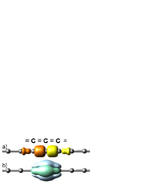
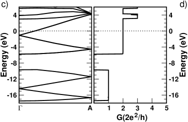
Fig. 3 and Fig. 4 show our results. Cumulene (Fig. 3a,b) is characterized by symmetric sp-bonds, uniformly distributed along the chain. states are localized in the middle of C-C bonds while states are centered around single C-atoms. In polyyne (4a,b), orbitals are localized both on single and on triple bonds, with a state in the middle of each bond. The orbitals are localized on the bonds: there are two of these orbitals in the middle of each triple bond, related by a 90∘ rotation around the axis.
The electronic structures and quantum conductances of cumulene and polyyne are shown in Fig. 3c,d and Fig. 4c,d respectively. The symmetric chain displays metallic behavior, in agreement with previous theoretical calculations. abdurahman Polyyne is instead semiconducting: the relaxation of the carbon-carbon distances induces a Peierls-type distortion, which stabilizes the structure and opens energy gaps at the edges of the Brillouin Zone. The metallicity of cumulene is an effect related to the homogeneous distribution of the atoms, and not to the dimensionality of the chain: polyyne, which has the same dimensionality of cumulene, is not a metal. As mentioned in the previous section, the electrical (metallic or semiconducting) behavior is tightly reflected in the geometrical properties of WFs. The eigenchannels of both systems, near the Fermi energy, are made by linear combination of the -like WFs of Figures 3-4b. As was the case for the aluminum chain, the orbitals of cumulene are located on the atoms, and the system is metallic. Contrary-wise, in polyyne the states are centered in the middle of the triple C-bonds, and the system is semiconducting.
IV Two terminal conductance
As a prototypical example of a two terminal device we have computed the quantum conductance for a small zigzag (5,0) carbon nanotube in the presence of an isolated substitutional silicon defect. Topological and substitutional defects in carbon nanotubes have been widely studied, choi ; chico ; andriotis ; kaun and our results can be directly compared with available theoretical data.
Using Fig. 1 as reference, we choose in the present case as the conductor region a finite segment of nanotube which contains the defect, while the leads are modeled by two semi-infinite nanotubes. To compute the two terminal conductance we need, in principle, three sets of calculations (two only if the leads are of the same material): bulk calculations for the two infinite leads and a supercell calculation for the conductor and the contacts (see Fig. 1). The supercell needs to be chosen large enough so that the influence of the conductor wavefunctions on the leads becomes negligible at the boundaries, assuring seamless matching between the lead WFs determined in the supercell and in the bulk calculations. The matching condition can also be expressed by saying that the on-site and hopping integrals (in the tight-binding language) of the individual WFs have to be the identical on both sides of the interface boundary. The matrices and for the infinite leads are obtained from the bulk calculations (in this case, the ideal (5,0) nanotube), while the other coupling matrices are derived from the supercell calculation. We stress the need to include a sufficiently large portion of the contacts in the supercell calculation so that, far from the interface and into the leads, the system recovers its bulk properties. The characteristic length determining the amount of conductor included is not the decay length of the density matrix of the metal (long-ranged, and algebraic), but the characteristic length of the WFs disentangled from the metal, and whose localization properties on these well-connected manifold are comparable to those of a semiconductor or an insulator. The properties of uniqueness and localization of the WFs ensure effortless continuity across the interface into the bulk leads. Note that a similar definition of the geometry of the simulation cell is needed also when using other real-space methods to compute quantum conductance.marco2 ; stokbro Since our supercell contains both the conductor and a portion of the leads large enough to take into account the presence of the contacts, the Wannier transformation produces a set of WFs covering the whole coupled region. However, since the WFs are strongly localized, it is straightforward to distinguish those centered on the conductor and those on the leads, and to see the matrix elements of the Hamiltonian seamless turn away from the conductor into bulk-like lead terms. This approach brings another advantage: since the conductor and the conductor-lead interfaces are simulated in the same supercell, we have a consistent (and fully relaxed) microscopic picture of the contacts.
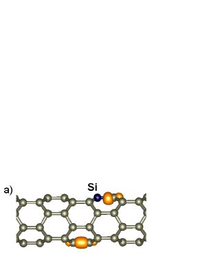
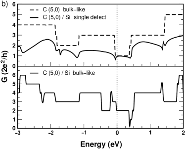
The (5,0) carbon nanotube (see Fig. 5a), has been simulated in a () Å3 supercell, with 8 k-points and a 40 Ry cutoff for the wavefunction expansion. Due to the highly localized nature of the WFs, only four atomic layers are needed to reproduce the bulk-like behavior of the nanotube far away from the Si defect. The presence of the defect does not induce significant structural relaxations, but affects the electronic and conduction properties of the tube. Figure 5a shows the isosurfaces of two calculated WFs with character. Far away from the defect, WFs are symmetric and centered in the middle of the C-C bond. Closer to the defect, the different electronegativity of silicon and carbon atoms induces a polarization of the Si-C bond that modifies the conduction properties of the system. Figure 5b (top panel) displays the quantum conductance of the nanotube with respectively in the presence of a defect (C(5,0)/Si, solid line) or in the ideal clean case (C(5,0), dashed line). The conductance of the ideal (5,0) nanotube shows the typical step-like shape and a metallic behavior, which is the result of the high curvature of such a small radius nanotube. blase ; gulseren Once a single Si defect is introduced, the system maintains its metallic character but the overall spectrum changes drastically. We observe a general reduction of the conductance along the whole energy range, and the distortion of the step-like shape of the pure nanotube. The appearance of dips, corresponding to the discontinuities in the original step function, is a characteristic feature of nanotubes with defects, choi ; chico ; kaun where the backscattering of electrons reduces the quantum conductance.
As a consequence of the external leads the quantum conductance is not directly related to the band structure of the supercell. We show this in Fig. 5b (bottom panel), where the bulk conductance of the C(5,0)/Si system is presented. The general trend of (E) is different from both curves in the upper panel. The whole C(5,0)/Si system is periodically repeated, and the conductance assumes the typical step-like behavior. However, with respect to the pure nanotube, we observe both an overall increse of the quantum conductance and the presence of novel features, such as the marked peak due to the silicon states, just below the Fermi level. The periodic distribution of the Si atoms leads to the formation of additional channels available for the charge transport along the tube. On the other hand, these features disappear in the case of the single defect, where the breaking of the traslational symmetry does not allow the formation of delocalized orbitals. In conclusion, while the doping with a regular pattern of Si-atoms increases the conductance, the scattering dephasing of a single defect reduces the global transport properties of the small carbon nanotube.
V Conclusions
We have presented a novel approach to calculate quantum conductance in extended systems in the coherent transport regime. Our methodology combines the accurate self-consistent minimization of the ground-state electronic structure via first-principles calculations, the determination of the maximally-localized WFs corresponding to manifold of bands spanning the energy range relevant for conduction, and the calculation of the quantum conductance using a real-space Green’s function formalism based on the Landauer approach. This procedure opens the way to selectively describe the quantum conductance in terms of the relevant one-electron states that contribute directly to the transport process. It links the description of electronic conductance to the intrinsic nature of the chemical bond, and gives new insights onto the essential mechanisms that govern the electron flow at the nanoscale. Moreover, it is computationally very efficient and can be straightforwardly implemented as a post-processing step in any standard electronic structure calculation web leading to a first-principles, highly accurate computation of electron transport properties.
As a first illustration of the potential of this methodology, we have studied quantum conductance in linear chains of aluminum and carbon atoms, and in defective carbon nanotubes. In all cases, we have underlined the effects of the reduced coordination and of the atomic relaxation on the transport properties and we have established a clear relationship between the electrical characteristics and the chemical bonds in the system.
VI Acknowledgments
We would like to thank Dr. Paolo Giannozzi and Dr. Carlo Cavazzoni for invaluable help and illuminating discussions. This work was supported in part by: MIUR (Italy) through grant FIRB-Nomade (A. C.); ONR grant N00014-01-1-1061 (N. M.), the Mathematical, Information and Computational Sciences Division, Office of Advanced Scientific Computing Research of the U.S. Department of Energy under contract No. DE-AC05-00OR22725 with UT-Battelle and the Petroleum Research Fund of the American Chemical Society (M. B. N.).
References
- (1) J. Nygard, D. H. Cobden, and P. E. Lindelof, Nature 408, 342 (2000).
- (2) J. Park, A. N. Pasupathy, J. Goldsmith, C. Chang, Y. Yaish, J. R. Petta, M. Rinkoski, J. P. Sethna, H. D. Abruna, P. L. McEuen, and D. C. Ralph, Nature 417, 722 (2002).
- (3) W. Liang, M. P. Shores, M. Bockrath, J. R. Long, and H. Park, Nature 417, 725 (2002).
- (4) A. Aviram and M. Ratner, ”Molecular Electronics: Science and Technology”, Ann. N.Y. Acad. Sci. 852 (1998); A. Aviram, M. Ratner, and V. Mujica, ”Molecular Electronics II”, Ann. N.Y. Acad. Sci. 960 (2002).
- (5) C. Joachim, J. K. Gimzewski, and A. Aviram, Nature 408, 541 (2000).
- (6) K. A. Williams, P. T. M. Veenhuizen, B. G. de la Torre, R. Eritja, and C. Dekker, Nature 420, 761 (2002).
- (7) M. S. Gudiksen, L.J. Lauhon, J. Wang, D. C. Smith, and C. Lieber, Nature 415, 617 (2002).
- (8) M. A. Reed, C. Zhou, C. J. Muller, T. P. Burgin, and J. M. Tour, Science 278, 252 (1997).
- (9) C. P. Collier, E. W. Wong, M. Belohradsky, F. M. Raymo, J. F. Stoddart, P. J. Kuekes, R. S. Williams, and J. R. Heath, Science 285, 391 (1999).
- (10) R. M. Metzger, Acc. Chem. Res. 32, 950 (1999).
- (11) E. Braun, Y. Eichen, U. Sivan, and G. Ben-Yoseph, Nature 391, 775 (1998); and K. Keren, M. Krueger, R. Gilad, G. Ben-Yoseph, U. Sivan, and E. Braun, Science 297, 72 (2002).
- (12) J. Reichert, R. Ochs, D. Beckmann, H. B. Weber, M. Mayor, and H. v. Löhneysen, Phys. Rev. Lett. 88, 176804 (2002).
- (13) R. H. M. Smit, Y. Noat, C. Untiedt, N. D. Lang, M. C. van Hemert, and J. M. van Ruitenbeek, Nature 419, 906 (2002).
- (14) J. Lahann, S. Mitragotri, T.-N. Tran, H. Kaido, J. Sundaram, I. S. Chaoi, S. Hoffer, G. A. Somorjai, and R. Langer, Science 299, 371 (2003).
- (15) S. J. Tans, M. H. Devoret, R. J. A. Groeneveld, and C. Dekker, Nature 394, 761 (1998); and S. J. Tans and C. Dekker, Nature 404, 834 (2000).
- (16) C. T. White, and T. N. Todorov, Nature 411, 649 (2001).
- (17) M. Ouyang, J.-L. Huang, C. L. Cheung, and C. M. Lieber, Science 292, 702 (2001).
- (18) P. G. Collins, M. S. Arnold, and P. Avouris, Science 292, 706 (2001).
- (19) N. Agraït, A. Levy Yeyati, and J. M. van Ruitenbeek, Phys. Rep. 377, 81 (2003).
- (20) H. Ohnishi, Y. Kondo, and K. Takayanagi, Nature 395, 780 (1998).
- (21) A. I. Yanson, G. Rubio Bollinger, H. E. van den Brom, N. Agraït, and J. M. van Ruitenbeek, Nature 395, 783 (1998).
- (22) N. Nilius, T. M. Wallis, and W. Ho, Science 297, 1853 (2002); and T. M. Wallis, N. Nilius, and W. Ho, Phys. Rev. Lett. 89, 236802 (2002).
- (23) R. Landauer, Philos. Mag. 21 863 (1970).
- (24) S. Datta, Electronic transport in mesoscopic systems (Cambridge Univ. Press 1995).
- (25) M. Buongiorno Nardelli, Phys. Rev. B 60, 7828 (1999).
- (26) T. N. Todorov, J. Hoekstra, and A. P. Sutton, Phys. Rev. Lett. 86, 3606 (2001).
- (27) P. S. Krstic, X.-G. Zhang, and W. H. Butler, Phys. Rev. B 66, 205319 (2002).
- (28) L. G. C. Rego, A. R. Rocha, V. Rodrigues, and D. Ugarte, Phys. Rev. B 67, 045412 (2003).
- (29) N. D. Lang, Phys. Rev. B 52, 5335 (1995); and M. Di Ventra, S. T. Pantelides, and N. D. Lang, Phys. Rev. Lett. 84, 979 (2000).
- (30) H. J. Choi and J. Ihm, Phys. Rev. B 59, 2267 (1999); and H.J. Choi and J. Ihm and S.G. Louie and M.L. Cohen, Phys. Rev. Lett. 84, 2917 (2000).
- (31) U. Landman, Proceedings of the Workshop on R&D Status and Trends in Nanoparticles, Nanostructured Materials, and Nanodevices in the United States, NSF, p. 192 (1997).
- (32) U. Landman, R. N. Barnett, A. G. Scherbakov, and P. Avouris, Phys. Rev. Lett. 85 1958 (2000).
- (33) Y.-G. Yoon, M. S. C. Mazzoni, H. J. Choi, J. Ihm, and S. G. Louie, Phys. Rev. Lett. 86, 688 (2001).
- (34) J. Taylor, H. Guo, and J. Wang, Phys. Rev. B 63, 245407 (2001).
- (35) S. N. Yaliraki, A. E. Roitberg, C. Gonzalez, V. Mujica, and M. A. Ratner, J. Chem. Phys. 111, 6997 (1999).
- (36) M. Brandyge, J.-L. Mozos, P. Ordejon, J. Taylor, and K. Stokbro, Phys. Rev. B 65, 165401 (2002).
- (37) J. J. Palacios, A. J. Pérez-Jemenez, E. Luis, E. SanFabián, and J. A. Vergés, Phys. Rev. B 66 035322 (2002).
- (38) S. Datta, Superlatticess and Microstructures 28, 253 (2000); and Y. Xue, S. Datta, and M. A. Ratner, J. Chem. Phys. 115, 4292 (2001).
- (39) A. Calzolari, R. Di Felice, E. Molinari, and A. Garbesi, Appl. Phys. Lett. 80, 3331 (2002).
- (40) F. L. Gervasio, P. Carloni, and M. Parrinello, Phys. Rev. Lett. 89, 108102 (2002).
- (41) R. Di Felice, A. Selloni, and E. Molinari, J. Phys. Chem B 107, 1151 (2003).
- (42) M. Buongiorno Nardelli and J. Bernholc, Phys. Rev. B 60, R16338 (1999).
- (43) M. Buongiorno Nardelli, J.-L. Fattebert, and J. Bernholc, Phys. Rev. B 64, 245423 (2001)
- (44) N. Marzari and D. Vanderbilt, Phys. Rev. B 56, 12847 (1997).
- (45) D. Lee and J. Jannopoulos, Phys. Rev. B 23, 4988 (1981).
- (46) F. Garcia-Moliner and V. R. Velasco, Theory of Single and Multiple Interfaces, (World Scientific, Singapore, 1992).
- (47) For the case of a metal we need to disentangle the states inside a given energy window from the rest of the Hilbert space, using the method described in Section II.3.
- (48) R. M. Dreizler and E. K. U. Gross, Density Functional Theory. An approach to the quantum many-body problem, (Springer-Verlag, Berlin 1990).
- (49) D. M. Ceperley and B. J. Alder, Phys. Rev. Lett. 45, 566 (1980); J. P. Pederw and A. Zunger, Phys. Rev. B 23, 5048 (1981).
- (50) N. Troullier and J. L. Martins, Phys. Rev. B 43, 1993 (1991).
- (51) L. Kleinman and D. M. Bylander, Phys. Rev. Lett. 48, 1425 (1982).
- (52) H. J. Monkhorst and J. D. Pack, Phys. Rev. B 13, 5188 (1976).
- (53) R. O. Jones and O. Gunnarsson, Rev. Mod. Phys. 61, 689 (1989).
- (54) E. Wimmer, Density Functional Approaches for Molecular and Materials Design, ACS Symposium Series 629, p. 423, edited by B. B. Laird, R. B. Ross, and T. Ziegler, American Chemical Society, Washington DC (1996).
- (55) Y. Lee, M. Buongiorno Nardelli and N. Marzari, to be published.
- (56) S. F. Boys, Rev. Mod. Phys., 32, 300 (1960).
- (57) P. L. Silvestrelli, N. Marzari, D. Vanderbilt, and M. Parrinello, Sol. Stat. Comm., 107, 7 (1998).
- (58) W. Kohn, Phys. Rev. 115, 809 (1959); and M. R. Geller and W. Kohn, Phys. Rev. B 48, 14085 (1993).
- (59) The minimization of the spread functional is obtained via a steepest descent scheme, in the reciprocal space. This procedure, computationally inexpensive, requires the updating only of the overlap matrices M, which appear in the formulation of the functional (M(k,b)) and of the matrices Uk(M(k,b)). For the complete description of the method see Ref. [44].
- (60) A group of bands are said to form a isolated composite group if they are inter-connected by degeneracy, but are isolated from all the other bands.
- (61) I. Souza, N. Marzari, and D. Vanderbilt, Phys. Rev. B 65, 035109 (2002).
- (62) is the result of the minimization procedure of Eq. 9; we dropped the suffix to simplify the notation.
- (63) D. Sánchez-Portal, E. Artacho, J. Junquera, P. Ordejón, A. García, and J. M. Soler, Phys. Rev. Lett. 83, 3884 (1999); and D. Sánchez-Portal, E. Artacho, J. Junquera, A. García, and J. M. Soler, Surf. Sci. 482, 1261 (2001).
- (64) S. R. Bahn and K. W. Jacobsen, Phys. Rev. Lett. 87, 26101 (2001); and S. R. Bahn, N. Lopez, J. K. Norskov, and K. W. Jacobsen, Phys. Rev. B 66, R081405 (2002).
- (65) H. Mehrez, A. Wlasenko, B. Larade, J. Taylor, P. Grütter, and H. Guo, Phys. Rev. B 65, 195419 (2002).
- (66) P. Sen, S. Ciraci, A. Buldum, and P. Batra, Phys. Rev. B 64, 195420 (2001).
- (67) J.-C. Zheng, H.-Q. Wang, A. T. S. Wee, and C. H. A. Huan, Int. J. Nanosci. 1, 159 (2002).
- (68) L. Ravagnan, F. Siviero, C. Lenardi, P. Piseri, E. Barborini, P. Milani, C. S. Casari, A. Li Bassi, and C. E. Bottani, Phys. Rev. Lett. 89, 285506 (2002).
- (69) N. D. Lang and Ph. Avouris, Phys. Rev. Lett. 81, 3515 (1998).
- (70) B. Larade, J. Taylor, H. Mehrez and H. Guo, Phys. Rev. B 64, 075420 (2001).
- (71) A. Abdurahman, A. Shukla, and M. Dolg, Phys. Rev. B 65, 115106 (2002).
- (72) B. Sporkmann and H. Bross, Phys. Rev. B 49, 10869 (1994).
- (73) M. Iannuzzi and M. Parrinello, Phys. Rev. B 66, 155209 (2002).
- (74) M. Brandbyge, M. Sorensen, and K. Jacobsen, Phys. Rev. B 56, 14956 (1997).
- (75) E. O. Fischer, On the road to carbene and carbyne complexes, Nobel Lecture (1973).
- (76) L. Kavan, Carbon 36, 801 (1998), and references therein.
- (77) T. Gibtner, F. Hampel, J. P. Gisselbrecht, and A. Hirsh, Chem. Eur. J. 8, 408 (2002).
- (78) L. Chico, L. X. Benedict, S. G. Louie, and M. Cohen, 54, 2600 (1996).
- (79) A. N. Andriotis, M. Menon, and D. Srivastava, J. Chem. Phys. 117, 2836 (2002).
- (80) C.-C. Kaun, B. Larade, H. Mehrez, J. Taylor, and H. Guo, Phys. Rev. B 65, 205416 (2002).
- (81) X. Blase, L. X. Benedict, E. L. Shirley, and S. G. Louie, Phys. Rev. Lett. 72, 1878 (1994).
- (82) O. Gülseren, T. Yildirim, and S. Ciraci, Phys. Rev. B 65, 153405 (2002).
- (83) The wannier code will soon be publicly released at http://www.wannier.org .