Quantum interference structures in the conductance plateaus of gold nanojunctions
Abstract
The conductance of breaking metallic nanojunctions shows plateaus alternated with sudden jumps, corresponding to the stretching of stable atomic configurations and atomic rearrangements, respectively. We investigate the structure of the conductance plateaus both by measuring the voltage dependence of the plateaus’ slope on individual junctions and by a detailed statistical analysis on a large amount of contacts. Though the atomic discreteness of the junction plays a fundamental role in the evolution of the conductance, we find that the fine structure of the conductance plateaus is determined by quantum interference phenomenon to a great extent.
pacs:
73.63.Rt, 73.23.Ad, 72.10.Fk, 72.15.LhThe investigation of the mechanical and electrical properties of atomic-sized metallic junctions has recently become an interesting topic of nanoscience (for a review see Ref. Agrait et al., 2003). A contact with a single atom in the cross section can be created by pulling a nanowire with a scanning tunneling microscope (STM) or the mechanically controllable break junction (MCBJ) technique. In such nanocontacts the coherent quantum phenomena always interplay with the atomic granularity of matter, as the wavelength of the electrons and the interatomic distance are in the same order of magnitude. The atomic nature of the junction is clearly demonstrated by the evolution of the conductance during the break of the contact showing plateaus alternated with sudden jumps (Fig. 1). Force measurements have shown that the conductance plateaus correspond to the stretching of stable atomic configurations, whereas the conductance jumps are related to atomic rearrangements.Rubio et al. (1996) On the other hand, the statistical analysis of a large amount of conductance vs. electrode separation traces has shown signs of conductance quantization in metals with loosely bound electrons.Krans et al. (1995) The quantum nature of conductance is also reflected by the quantum interference (QI) phenomenon of the electron waves scattered on nearby impurities, which was reported in Refs. Ludoph et al., 1999; Untiedt et al., 2000. These works investigated the interference patterns in the voltage dependence of the conductance. In this paper we demonstrate that QI has a definite influence on the structure of the conductance plateaus as well, which arises due to the spatial variation of the electron paths during the stretching of the junction.
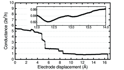
The measurements were performed on high purity gold samples at liquid Helium temperature with the MCBJ technique.Agrait et al. (2003) The conductance histogram of Au shows a sharp peak at the quantum conductance unit, G. This peak arises from the frequent occurrence of plateaus that are accurately positioned at G0, as shown in Fig. 1. It was found, that these plateaus are related to the conductance through a single gold atom,Agrait et al. (2003) or through a chain of gold atoms in a row.Yanson et al. (1998) In both cases the contact has a single conductance channel with almost perfect transmission.Scheer et al. (1998); Rubio-Bollinger et al. (2003) Theoretical studies have pointed out that in gold the conductance of a monoatomic contact is not sensitive to the amount of stretching, which could explain the flatness of the last conductance plateau.Cuevas et al. (1998) In the experiments, however, the conductance plateaus always show a fine structure, which are different during each rupture (for examples see Ref. Untiedt et al., 2000 and the inset in Fig. 1). This feature could be naturally explained by the atomic discreteness of the junction: as the electrodes are pulled apart the overlap between the central atoms changes, which alters the conductance of the contact. In this paper we show that this interpretation is not satisfactory, and the fine structure of the conductance plateaus is strongly affected by quantum interference phenomenon.
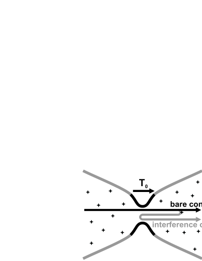
The basic idea behind quantum interference in atomic-sized junctions is illustrated in Fig. 2. The narrow neighborhood of the contact center can be considered as a ballistic region with a transmission probability, . The electron wave that has travelled through the contact can be partially reflected by impurities or lattice defects farther away in the diffusive electrodes. This reflected wave goes back to the contact, and a part of it is reflected back again by the contact itself. This part of the wave interferes with the direct wave, modifying the conductance of the junction. The net transmission including the interference corrections can be written as:
| (1) | |||
The total transmission is a function of the electrode separation, and the bias voltage, . The bare transmission of the contact, is controlled by the shape of the junction and the overlap between the atomic orbitals, and accordingly it is dependent on the electrode separation, . It was shown that in the voltage scale of the measurement the voltage dependence of can be neglected.Nielsen et al. (2002); Brandbyge et al. (2001) In the interference correction the sum runs over the various electron trajectories; and are respectively the path length and the phase shift on a trajectory; and is the Fermi wave number. The amplitude is determined by the scattering cross section of the defect, the length of the path, and the reflection of the contact. The differential conductance of the system is obtained from the transmission as G. (For the sake of simplicity, a single conductance channel is considered. The argumentation would be similar for multiple channels as well.)
Quantum interference results in fluctuations in the conductance when the interference conditions are tuned experimentally. If the wave number of the electrons is changed by the bias voltage, QI shows up as a small, random oscillation in the curve.Ludoph et al. (1999); Untiedt et al. (2000) The interference pattern can also be changed by tuning the phase factor of the electron paths with magnetic field. In atomic-sized contacts, however, a magnetic field of T would be required to have a considerable influence on the interference, while a field of T already causes changes in the atomic arrangement of the contact due to magnetostriction effects.Ludoph (1999) Here, we focus our attention on quantum interference due to the variation of the length of the electron paths. In nanojunctions the path length naturally changes with the separation of the electrodes. To have a complete period in the interference pattern the electrode separation should be changed by one wavelength of the electrons. Experimentally, such a displacement is not possible without a jump-like atomic rearrangement, which abruptly changes the interference pattern. From this reason, only shorter parts of the conductance plateaus can be studied, like that in the inset of Fig. 1. The fine structure of these short segments can originate both from the QI phenomenon and from the electrode separation dependence of the bare transmission, . In the following we show experimental techniques, that can tell “to what extent these two phenomena are involved in the evolution of the plateaus”. To investigate the fine structure of the conductance traces, we have studied the local slope of the plateaus by two different methods.
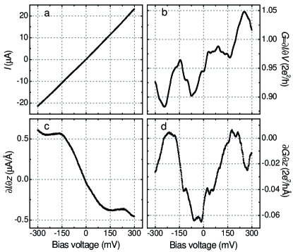
The first approach examines the effect of bias voltage on the plateaus’ slope on individual junctions. Figure 3 shows the current (panel a), and the derivative of the current with respect to the electrode separation (panel c) recorded as a function of the bias voltage. The two curves were measured simultaneously on the same junction. The electrode separation was modulated by applying a sine-wave voltage on the piezo element. The oscillation of the separation had a typical amplitude of Å. As the bias voltage was varied, the current was detected both by a current meter measuring the DC component and a lock-in amplifier recording the response to the modulation. The signal of the current meter provided the curve, whereas the lock-in measured the value of . The differential conductance, and the slope of the plateau, was determined by numerical differentiation (Fig. 3b and 3d, respectively). These curves are reproducible to the very small details as long as the same contact is measured. When the junction is changed a completely new structures appear in the curves, as expected from QI phenomenon.
Assume that the dependence of the differential conductance on the electrode separation, is attributed solely to the bare transmission . In this case the slope of the conductance plateau can be written as:
| (2) |
i.e. the voltage dependence of is simply proportional to . This, however is disproved by the experimental results shown above. The oscillatory patterns of the curve and the curve in Fig. 3 do not coincide. Furthermore, in the curve the oscillations have a typical amplitude of compared to the mean value of G0, while in the curve the relative amplitude of the oscillations is more than 10 times larger.
These observations can only be explained, if the change of the path lengths is also taken into account as the electrode separation is varied by . Then, the derivative of the transmission with respect to is written as:not (a)
| (3) | |||
Based on this formula, is well approximated with the mean value of the curve, which is Å-1. The amplitude of the interference correction is characterized by the standard deviation: Å-1. It shows, that the variation of the plateau’s slope due to QI is comparable to the separation dependence of the bare transmission. The comparison of the formulas (1) and (3) shows, that the amplitude of the oscillatory term changes by a factor of , while the constant term changes by due to the differentiation. According to measurements on several contacts, is typically below Å-1, which is smaller by an order of a magnitude than Å-1. This explains that the contribution of QI is highly enhanced in the curves, while in the curve it only gives a minor correction.
The above measurements were performed on individual contacts. In the following we present a second approach, investigating the statistical properties of the slope of the conductance plateaus. Independent atomic configurations with different set of the interference parameters (, and ) can be naturally created by repeating the break of the junction several times. The data set for the statistical analysis was obtained by recording independent conductance vs. electrode separation traces at fixed bias voltage. The typical acquisition rate was points/Å. The slope of the plateaus was determined by numerical differentiation. The derivative was calculated at each point of the conductance plateaus, however the jump-like changes between two plateaus – corresponding to sudden atomic rearrangements – were excluded from the analysis.
In the mean value of the interference corrections cancel out due to their random distribution around zero, thus the average slope of the plateaus is only determined by the bare transmission:
| (4) |
The proper quantity to study QI is rather the mean square deviation of , which contains the interference term beside the properties of the bare contact (see Eq. 3):
| (5) |
The squared amplitude, is proportional to the probability that an electron is reflected back by the contact, . Therefore, the interference term in the mean square deviation vanishes both at and .
Gold junctions with a few atoms () in the cross section show the saturation of the channel transmissions, which means that a new channel only starts to open, if the previous ones are almost completely open. Due to this behavior at the quantized conductance values all transmission probabilities are close to unity or zero, thus the quantum interference is suppressed.Ludoph et al. (1999) If QI gives a detectable contribution to the slope of the plateaus, the curves should also exhibit the quantum suppression at the multiples of G0. This phenomenon is clearly resolved in our experiments: the mean square deviation of the plateaus’ slope exhibit pronounced minima accurately placed at and G0 (Fig. 4a). In contrast, the second and the third peak in the conductance histogram are significantly shifted from the integer values (Fig. 4c). It demonstrates that the minima in are a consequence of a pure quantum phenomenon, and they are not related to the preferred atomic configurations shown by the peaks in the histogram.
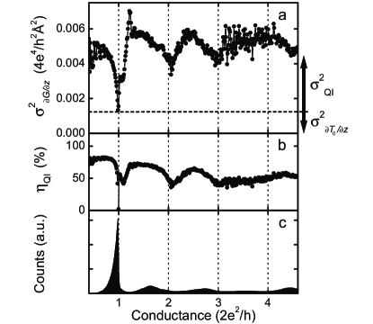
The suppression of QI at the quantized values gives a possibility to estimate the contribution of the quantum interference term to the slope of the plateaus. According to Ref. Ludoph et al., 1999 the magnitude of the quantum suppression is almost at G0, while at higher quantized values it is decreasing. Therefore, we attribute the nonzero minimum value of at G0 purely to the scattering of the bare properties, . The interference term in Eq. 5, is approximated by subtracting , which is considered as a constant background.not (c) The relative amplitude of QI in the slope of the plateaus can be characterized by the quantity . This curve takes values larger than (Fig. 4b), which demonstrates that the influence of QI on the slope of the plateaus is dominating over the features due to the atomic arrangement of the bare contact.
For a more quantitative description of the observations we have performed a calculation following the model in Ref. Ludoph et al., 1999. In the limit the standard deviation of the plateau’s slope due to the QI terms can be written as:
| (6) |
This formula already treats a multichannel situation, where is the transmission of the -th channel, is the opening angle of the contact, and is the elastic mean free path of the electrons. From the measured amplitude of the elastic mean free path is estimated as nm, which is in good agreement with previous results.Ludoph et al. (1999)
Concluding, we have investigated the structure of the conductance plateaus in gold nanocontacts. We have studied the voltage dependence of the slope of the conductance plateaus on individual junctions. The curves have shown a strong oscillatory deviation from the mean value, which is an order of a magnitude larger than the conductance fluctuations in the G(V) characteristics. This feature could only be described by quantum interference due to the spatial modulation of the interference paths. In order to support these results we have performed a statistical analysis of the plateaus’ slope for a large amount of junctions. The quantum suppression of at the quantized conductance values have provided an even stronger proof for the significant presence of QI. With our analysis the contributions of quantum interference and the strain dependence of the local atomic configuration to the plateaus’ slope could be separated. The results have shown that the quantum interference phenomenon and the atomic discreteness of the junction have a similarly strong influence on the fine structure of the conductance plateaus.
The authors acknowledge the financial support from the “Stichting FOM” and the Hungarian research funds OTKA TS040878, T037451.
References
- (1)
- (2) [†] Also at: B. Verkin Institute for Low Temperature Physics & Engineering, National Academy of Science of Ukraine, 47 Lenin Av., 61164, Kharkov, Ukraine.
- Agrait et al. (2003) N. Agrait, A. L. Yeyati, and J. M. van Ruitenbeek, Phys. Rep. 377, 81 (2003).
- Rubio et al. (1996) G. Rubio, N. Agrait, and S. Vieira, Phys. Rev. Lett. 76, 2302 (1996).
- Krans et al. (1995) J. M. Krans, J. M. van Ruitenbeek, V. V. Fisun, I. K. Yanson, and L. J. de Jongh, Nature 375, 767 (1995).
- Ludoph et al. (1999) B. Ludoph, M. H. Devoret, D. Esteve, C. Urbina, and J. M. van Ruitenbeek, Phys. Rev. Lett. 82, 1530 (1999); B. Ludoph and J. M. van Ruitenbeek, Phys. Rev. B 61, 2273 (2000).
- Yanson et al. (1998) A. I. Yanson, G. R. Bollinger, H. E. van den Brom, N. Agrait, and J. M. van Ruitenbeek, Nature 395, 783 (1998).
- Cuevas et al. (1998) J. C. Cuevas, A. L. Yeyati, A. Martin-Rodero, G. R. Bollinger, C. Untiedt, and N. Agrait, Phys. Rev. Lett. 81, 2990 (1998).
- Nielsen et al. (2002) S. K. Nielsen, M. Brandbyge, K. Hansen, K. Stokbro, J. M. van Ruitenbeek, and F. Besenbacher., Phys. Rev. Lett. 89, 066804 (2002).
- Brandbyge et al. (2001) M. Brandbyge, N. Kobayashi, and M. Tsukada, Phys. Rev. B 60, 17064 (2001).
- Untiedt et al. (2000) C. Untiedt, G. Rubio Bollinger, S. Vieira, and N. Agrait, Phys. Rev. B 62, 9962 (2000).
- Scheer et al. (1998) E. Scheer, N. Agrait, J. C. Cuevas, A. L. Yeyati, B. Ludoph, A. Martin-Rodero, G. Rubio-Bollinger, J. M. van Ruitenbeek, and C. Urbina, Nature 394, 154 (1998).
- Rubio-Bollinger et al. (2003) G. Rubio-Bollinger, C. de las Heras, E. Bascones, N. Agrait, F. Guinea, and S. Vieira, Phys. Rec. B 67, 121407 (2003).
- Ludoph (1999) B. Ludoph, Ph.D. thesis, Universiteit Leiden, The Netherlands (1999).
- not (a) In the experiments the applied voltage is much smaller than the Fermi energy, so the term was neglected beside . The term was also neglected being an order of a magnitude smaller than .
- not (c) If is assumed to be constant in the whole conductance range, the relative amplitudes of the minima in are similar to those in Ref. Ludoph et al., 1999. This agreement suppurts our assumption. As a further verification, we have also performed measurements on polyvalent metals, for which no suppression of QI occurs at the quantized values,Ludoph et al. (1999) thus any special structure in the dependence of should come from the bare properties. In these measurements the variation of was found to smaller than of the total signal.