Group-V mixing effects in the structural and optical properties of
Abstract
We present ab initio total energy and band structure calculations based on Density Funtional Theory (DFT) within the Local Density Aproximation (LDA) on group-V mixing effects in the optoelectronic material . This compound has been recently proposed by theoretical design as an optically active material in the 1.5 m (0.8 eV) fiber optics frequency window and with a monolithic integration with the Si (001) surface. Our results indicate that alloy formation in the group V planes would likely occur at typical growth conditions. In addition, desired features such as in-plane lattice constant and energy gap are virtually unchanged and the optical oscillator strength for band-to-band transitions is increased by a factor of 6 due to alloying.
pacs:
v9-32.tex – PACS: 71.15.Nc, 85.60.BtI Introduction
The monolithic integration between electronic and optically active materials has been strongly pursued by the optoelectronics industry review . Typical III-V and II-VI alloys, commonly used in the band gap engineering of optoelectronic devices, present a polarity mismatch harrison for integration with group-IV materials surfaces in the chemical bonding level , i.e., heteroepitaxial depositions of group-V(III) atoms followed by group-III(V) atoms on group-IV (001) surface produce an excess (a lack) of electrons to make the chemical bonds. Moreover, none of these alloys do not satisfy constraints of having both lattice matching to silicon a direct band-gap in the 1.5 m frequency range.
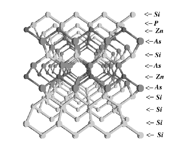
The growth sequence of group elements V-II-V-IV proposed recently by Wang et al. wang1 ; wang2 could solve all these problems. The compound was proposed after extensive theoretical exploration of several possible V-II-V-IV materials. The new optoelectronic material could be grown using the heteroepitaxy sequence As-Zn-As-Si-As-Zn-P-Si on a Si (001) surface, as shown in Fig. 1. This particular proportion between As and P optimizes the lattice constant, the direct energy-gap and the polarity at the same time, although a residual dipole moment is left due to chemical difference between P and As. Wang et al. wang1 ; wang2 proposed to eliminate this dipole inverting every other cell in the growth direction.
In this work, we explore the possibility of mixing As and P in the same growth plane in a 3:1 rate instead of growing sequences of planes containing only As or only P. Group-V mixing would automatically eliminate any residual dipole moment. Besides, it could provide a simpler way to fine-tune the material’s properties (like the band gap and the lattice constant). Moreover, in real growth conditions, group-V mixing could be unavoidable due to the similar chemical characteristics of P and As. Of course, it remains to be shown that the disordered alloy retains the desired features of the ordered material, and this is the purpose of this work.
We perform ab-initio total-energy, band structure and optical oscillator strength calculations based on Density Functional Theory (DFT) and the pseudopotential method. We compare the calculated properties of the originally designed and three forms that mix As and P in the same epitaxial growth plane. We also perform calculations on the ”precursor” materials , and in order to understand the electronic structure features in the familly V-II-V-IV materials and their influence in the optical oscillator strength.
II Methodology
The present results have been obtained thanks to the ABINIT code gonze ; ABINIT , that is based on pseudopotentials and planewaves. It relies on an efficient Fast Fourier Transform algorithm FFT for the conversion of wavefunctions between real and reciprocal space, on the adaptation to a fixed potential of the band-by-band conjugate gradient method payne and on a potential-based conjugate-gradient algorithm for the determination of the self-consistent potential gonze2 .
We use DFT within the local-density approximation (LDA) hohenberg ; kohn . We adopt the exchange-correlation functional parametrized by Perdew and Zunger perdew from Ceperley and Alder’s ceperley data for correlation energy of the homogeneus electron gas. We use the scheme of Troullier and Martins tm to generate soft norm conserving pseudopotentials. The semi-local pseudopotentials are further transformed into fully separable Kleinman-Bylander pseudopotentials kleinman , with the potential chosen as the local potential. For Zn atoms we use non-linear core corrections and an excitated and ionized configuration . The pseudopotentials have been generated by the FHI98PP code FHI98PP . The wave functions are expanded in a plane wave basis with maximum kinetic energy of 40 Ry. Brillouin-Zone summations are carried out in Monkhorst-Pack (4 x 4 x 4), (4 x 4 x 2) and (2 x 2 x 4) -point sampling grid for precursors, and alloys, respectively.
Calculations are performed for the precursors , and (4 atoms per unit cell), the originally proposed (eight atoms per unit cell) and three distinct configurations of ”alloys” (16 atom per unit cell) that mix As and P in the same plane. The three alloy configurations (A-1, A-2 and A-3) are shown in Fig. 2. The A-1 configuration has two planes with As:P 3:1, the A-2 and A-3 have one plane with four As and one plane with As:P 2:2 in two inequivalent configurations.
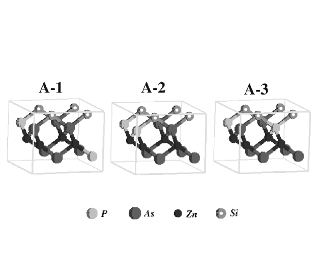
As one can see, the A-2 and A-3 structures are not primitive, but we use the supercells shown in Fig. 2 in order to facilitate comparisons among all three alloy structures. Of course, only A-1 contains As:P 3:1 in each group-V plane, as we propose. But the other two are also important to study trends in the materials’ properties due to composition fluctuations. The equilibrium lattice parameters for all structures are found by minimizing the total energy. For each set of lattice parameters the relative ion positions are relaxed until the forces are smaller then 10-6 Hartree/Bohr.
III Results and Discussion
When fully relaxed, the alloy structure A-1 has a primitive monoclinic Bravais lattices (space group ), but with very small deviations from a tetragonal unit cell: Differences in the in-plane lattice constants are smaller than 0.01 Å ( Å), and the angle between the respective lattice vectors is . Structures A-2 and A-3 are primitive orthorhombic (space group ) and base-centered orthorhombic (space group Cmm2), respectively, with Å and Å in both cases. Therefore, they also present very small deviations from tetragonal () symmetry. When considering epitaxial growth of disordered alloy structures on top of a Si substrate, tetragonal symmetry will be very naturally imposed. Therefore, in the remainder of this article, we will adopt a tetragonal symmetry constraint.
| Unit cell | (Å) | (Å) | mismatch (%) | (eV) |
|---|---|---|---|---|
| 3.81 | 10.91 | -0.2 | 0.001 | |
| A-1 | 7.59 | 5.46 | -0.4 | -0.003 |
| A-2 | 7.59 | 5.46 | -0.4 | -0.002 |
| A-3 | 7.59 | 5.46 | -0.4 | -0.002 |
Table I shows the calculated tetragonal lattice constants ( and ), the in-plane lattice mismatch with respect to Si and the formation energies for the compound and the A-1, A-2 and A-3 alloys. The mismatch is for unmixed and for the alloys, where is the in-plane lattice constant for the new materials and is the Si lattice constant multiplied by . Our results show that the in-plane mismatch for all alloy structures are very small, suggesting that disorder in the group-V planes leads to structures that can be monolithically integrated to Si as easily as the originally proposed ordered material.
The relative formation energies per group-V atom for the alloys and the compound are calculated with respect to the precursor compounds and , i.e., they define the enthalpy of mixing different group-V elements. As one can see, all values are extremely small, slightly negative for the alloys (from -2 to -3 meV) and slightly positive for . These small values allow us to safely state that structures with the same proportion of As and P are essentially degenerate in energy, regardless of the particular atomic arrangement. Moreover, this suggests that, at typical growth temperatures, disordered structures will have lower free energy due to their higher configurational entropy.
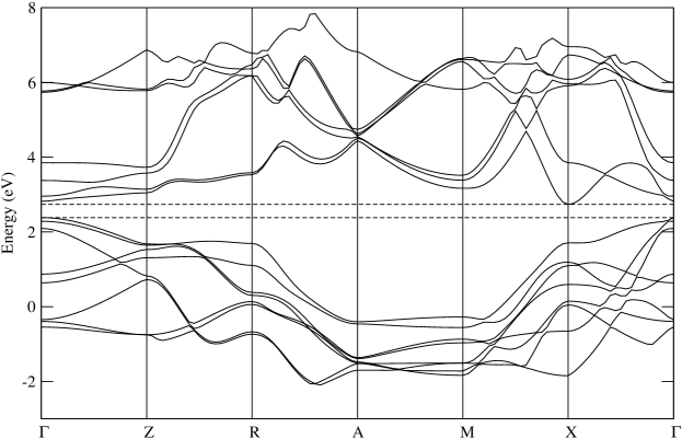
We now focus on the group-V mixing effects in the band structure of these materials. Fig. 3 shows the band structure of the compound. Within LDA this compound has a marginally indirect gap, with valence band maximum at and conduction band minimum at . Quasi-particle corrections make it a direct-gap material with a 0.8 eV energy gap at wang1 ; wang2 . Table II shows and energy gaps for the compound and the three alloy configurations. Clearly, the energy gaps at and are not affected too much by group-V mixing comment . Moreover, the LDA ”indirectness” (measured by the () - () gap difference) is also essentially unaffected. From these considerations, it is likely that corrections will also be similar in all these structures, and we may expect that alloys with As:P 3:1 proportion will also have a direct band-gap around 0.8 eV. More important, the tayloring of structures with group-V mixing provides an easier way to ”fine-tune” the the gap energy so that matches exactly the 1.5 m fiber optics window.
| Unit cell | ||||
|---|---|---|---|---|
| 0.438 | 0.353 | 0.085 | 1.00 | |
| A-1 | 0.552 | 0.463 | 0.089 | 6.04 |
| A-2 | 0.498 | 0.393 | 0.105 | 1.22 |
| A-3 | 0.523 | 0.391 | 0.133 | 1.16 |


A direct gap is not enough to guarantee efficient emission properties. In addition, one has to ensure a high optical oscillator strenght (OOS) between the initial and final states. Table II also shows the calculated OOS for conduction to valence transitions at , given by:
| (1) |
where is the momentum, is the gap energy and is the mass of the electron. The values are normalized by for the compound. The results show that the alloy with As:P 3:1 in each plane containing V-atoms (A-1) is the best emitter. Comparing with the , the OOS is multiplied by six. The configurations A-2 and A-3 have higher OOS’s than too, but only by 16% and 22%, respectively. This result is striking, because in general one naively expects that disorder tends to decrease OOS’s, but we shall see that it can be explained from a simple analysis of the electronic density profiles of valence and conduction states for the structures.
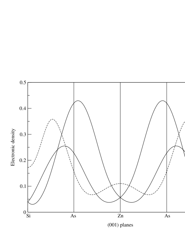
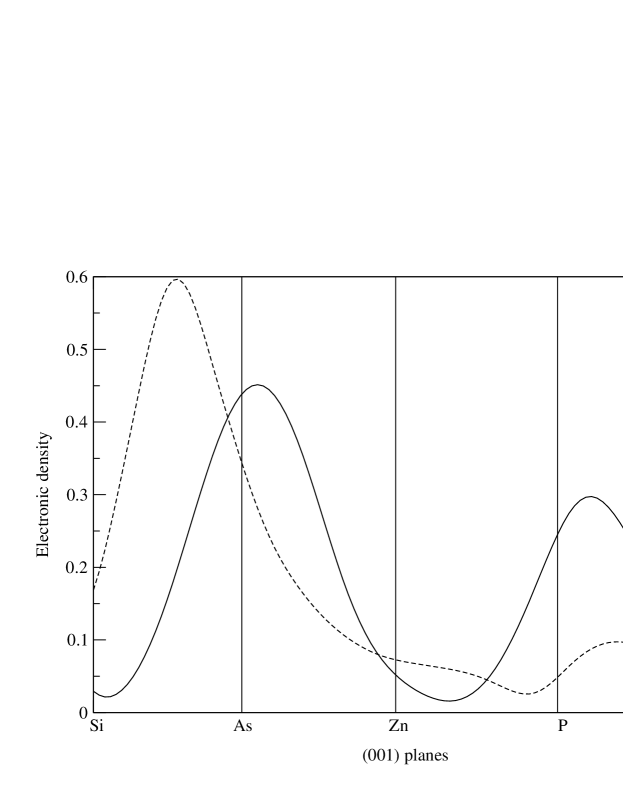
First of all, it is instructive to analyze the density profiles of band-edge states for the precursors and in the Figs. 4 and 5, respectively. These figures show the projected electronic density on the growth axis (i. e., averaged over the planes). The top of the valence band in the precursor is doubly degenerated, with most of the charge in the As planes as shown in Fig. 4. In fact, the electrons in these bands are mainly in linear combinations of and atomic orbitals as shown in Fig. 6. Fig. 4 also shows that the density from the conduction band of is peaked between Si and As atomic planes. Indeed, it is formed by antibonding states between As and Si (Fig. 7).
When one of the As planes is replaced by a P plane to form , the degeneracy in the top of the valence band is broken and the symmetry of conduction electronic density too, as show in Fig. 5. The valence band charge is now mostly on the As planes and the conduction band one is between Si and As planes.
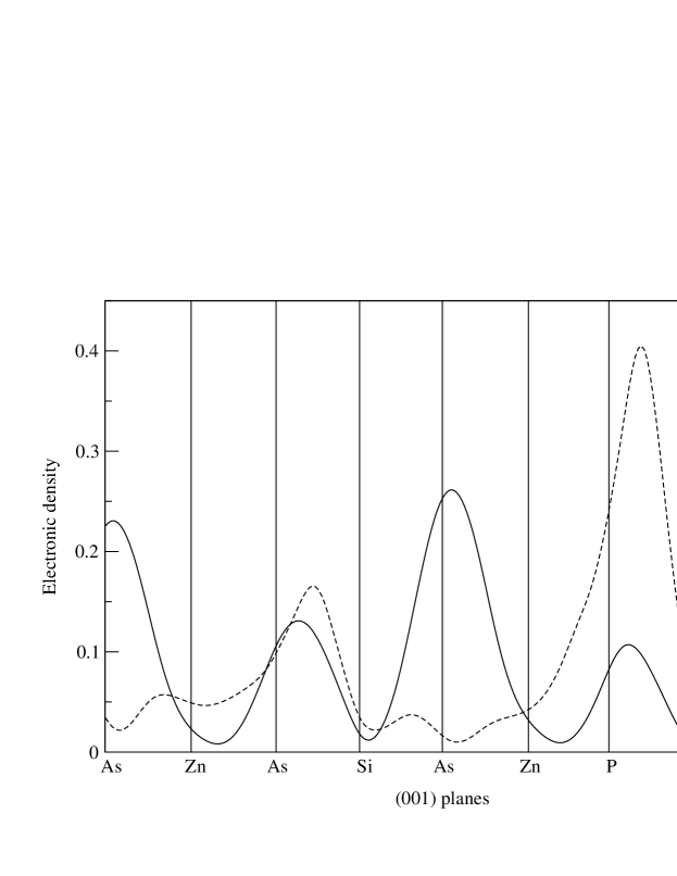
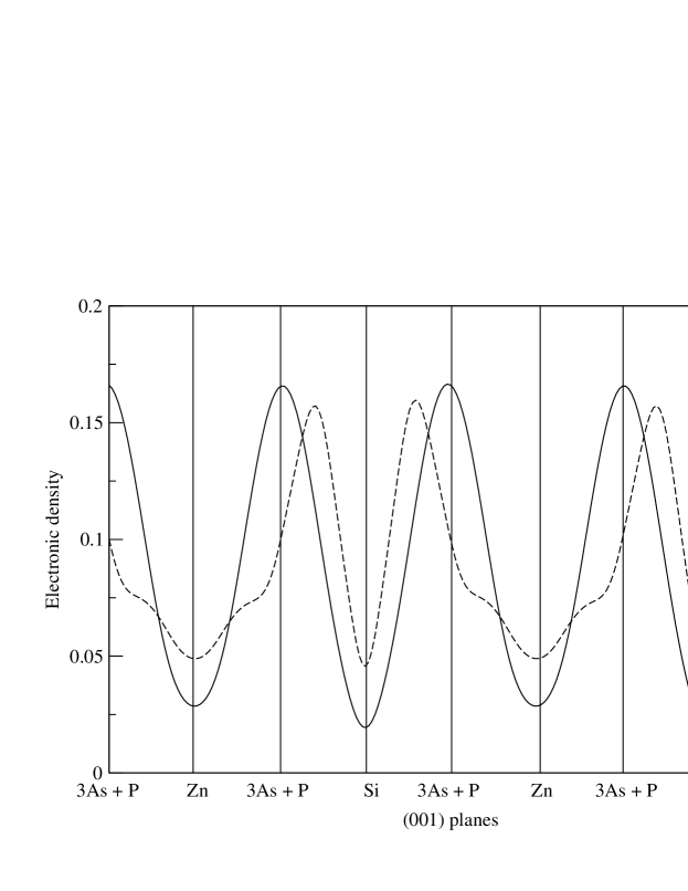
The density profiles for the compound and related alloys seem to obey the precursors’ general scheme. None of these structures has energy degeneracy in the top of the valence band. The valence band electrons are mainly near the group-V planes and the conduction band electrons are antibonding states between Si-As or Si-P, for all configurations. For (Fig. 8), the charge density maxima at the valence band alternate their intensities like in the precursor , but the conduction band electrons are mostly located between the Si and P planes. There is a significant difference between A-1 and the ordered , since all group-V planes are identical. Because of that, the valence band electronic densities at these planes are all the same, as shown in Fig. 9. The density of the antibonding states at conduction band is also evenly distributed between all equivalent group-V planes and Si planes. We can clearly note that the overlap between top valence states and the conduction states in the A-1 alloy is much larger than originally proposed compound. That is the reason why the OOS for the A-1 alloy is much higher than that of the compound.
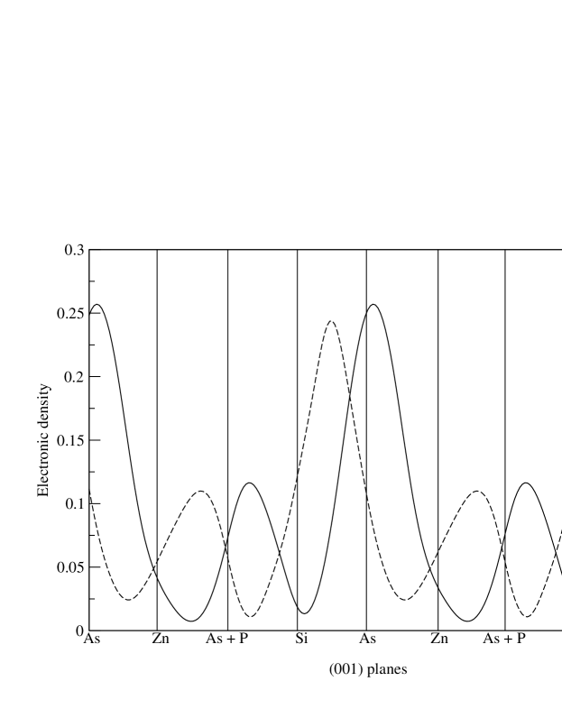
For the alloy configuration A-3, the densities of valence and conduction charge (Fig. 10) clearly show an intermediate overlap if compared to A-1 and . The situation is very similar for the configuration A-2. From all these results, we can extract the following trend for valence-conduction overlap in real space: A-1 A-3 A-2 , which, therefore explains the trend in OOS’s shown in Table II . As a general statement, we can say that a more homogeneous distribution between As and P atoms in the group-V planes is the key to maximize the emission properties of this class of materials. footnote
IV Conclusions
In conclusion, we have calculated the total energy, geometry, optical oscillator strength, band structure and electronic densities profiles of as an ordered material and in three alloy configurations in order to study the group-V mixing effect on the properties of this new optoelectronic material. Our results indicate that the relevant structural (in-plane lattice matching to Si) and optical (band gap at 0.8 eV) properties are kept in the presence of group-V atomic mixing. Very small energy changes between different configurations suggests that, at growth temperatures, random occupation of group-V planes would minimize the free energy. The mixing would allow fine-tuning of the band gap energy. The calculated optical oscillator strengths suggest that the structure with As and P at 3:1 rate in all group-V planes would be six times more optically active than the structure originally proposed, with As and P in different (001) planes.
Acknowledgements.
This work was supported by the following Brazilian funding agencies: Conselho Nacional de Desenvolvimento Científico e Tecnológico (CNPq), Fundação Carlos Chagas Filho de Amparo à Pesquisa do Estado do Rio de Janeiro (FAPERJ), Fundação Universitária José Bonifácio (FUJB-UFRJ), Instituto do Milênio de Nanociências and Programa de Núcleos de Excelência (PRONEX-MCT).References
- (1) Heteroepitaxy in Silicon II, edited by J. Fan, J. Phillips, and B.-Y. Tsaur, MRS Symposia Proceedings No. 91 (Materials Research Society, Pittsburgh, 1987).
- (2) W. A. Harrison, E. A. Kraut, J. R. Waldrop and R. W. Cront, Phys. Rev. B 18, 4402 (1978).
- (3) T. Wang, N. Moll, K. Cho, J. D. Joannopoulos, Phys. Rev. Lett. 82, 3304 (1999).
- (4) T. Wang, N. Moll, K. Cho, J. D. Joannopoulos, Phys. Rev. B 63, 035306 (2000).
- (5) X. Gonze, J.-M. Beuken, R. Caracas, F. Detraux, M. Fuchs, G.-M. Rignanese, L. Sindic, M. Verstraete, G. Zerah, F. Jollet, M. Torrent, A. Roy, M. Mikami, Ph. Ghosez, J.-Y. Raty, and D. C. Allan, Computational Materials Science 25, 478-492 (2002).
- (6) The ABINIT code is a common project of the Université Catholique de Louvain, Corning Incorporated, and other contributors (URL http://www.abinit.org).
- (7) S. Goedecker, SIAM J. on Scientific Computing 18, 1605 (1997).
- (8) M. C. Payne, M. P. Teter, D. C. Allan, T. A. Arias and J. D. Joannopoulos, Rev. Mod. Phys. 64, 1045 (1992). ,
- (9) X. Gonze, Phys. Rev. B 54, 4383 (1996).
- (10) P. Hohenberg and W. Kohn, Phys. Rev. 136, 864B (1964).
- (11) W. Kohn and L. J. Sham, Phys. Rev. 140, 1133A (1965).
- (12) D. M. Ceperley and B. J. Alder, Phys. Rev. Lett. 45, 566 (1980).
- (13) J. P. Perdew and A. Zunger, Phys. Rev. B 23, 5048 (1981).
- (14) N. Troullier and J. L. Martins, Phys. Rev. B 43, 1993 (1991).
- (15) L. Kleinman and D. J. Bylander, Phys. Rev. Lett. 23, 1425 (1982).
- (16) M. Fuchs and M. Scheffler, Comput. Phys. Commun. 119, 67 (1999).
- (17) It is important to notice that 0.1 eV energy differences are within the error bars of either LDA and GW band structures.
- (18) In any structure where As and P are present, the bottom of the conduction band is either localized between Si and As (for example, , Fig. 5) or between Si and P (for example, , Fig. 8). Interestingly, we find that even small changes in geometry can modify the real-space localization of this state: We performed calculations on using the in-plane lattice parameter of and that shifts the energy ordering between Si-As and Si-P states so that the bottom of the conduction band becomes localized in Si-P. Therefore, for a given ordered system it should be hard to predict the exact real-space localization of the conduction band state. However, our conclusion remain valid: In a disordered alloy with a 3/1 As/P ratio, we should expect an even distribution of the conduction band electrons among the group-V planes, leading to a larger OOS as compared to the ordered compound .