Geometrical enhancement of the proximity effect in quantum wires
with extended superconducting tunnel contacts
Abstract
We study Andreev reflection in a ballistic one-dimensional channel coupled in parallel to a superconductor via a tunnel barrier of finite length . The dependence of the low-energy Andreev reflection probability on reveals the existence of a characteristic length scale beyond which is enhanced up to unity despite the low interfacial transparency. The Andreev reflection enhancement is due to the strong mixing of particle and hole states that builds up in contacts exceeding the coherence length , leading to a small energy gap (minigap) in the density of states of the normal system. The role of the geometry of such hybrid contacts is discussed in the context of the experimental observation of zero-bias Andreev anomalies in the resistance of extended carbon nanotube/superconductor junctions in field effect transistor setups.
pacs:
74.45.+c, 74.50.+r, 73.23.Ad.I Introduction
The interest in proximity-induced superconductivity in one-dimensional (1D) electron systems Fazio ; Maslov ; Takane ; Affleck ; Wei ; Titov ; Gonzalez ; Vish ; Nikolic ; Lee ; Jiang ; Vecino ; Tanaka has recently revived in the light of successful experiments on electron transport through carbon nanotubes contacted by superconductors Kasumov ; Morpurgo ; Schoenen ; Haruyama . Despite possibly strong electron-electron interactions Schoenen ; Bockrath , in many situations transport properties of metallic single-walled carbon nanotubes can be interpreted within a ballistic model assuming two conduction bands at the Fermi level Dres . Hence, superconductor/carbon nanotube (S/CN) junctions can to some extent be viewed as an experimentally accessible case of 1D ballistic proximity structures Morpurgo .
Like in conventional normal metal/superconductor (N/S) junctions, the extent to which the proximity effect modifies the electronic properties of carbon nanotubes strongly depends on the quality of S/CN interfaces. In S/CN/S junctions with highly nontrivial end-bonding of the tubes it is possible to achieve high transparency contacts and observe induced supercurrents between the S banks Kasumov ; Schoenen ; Haruyama . In a more conventional field-effect transistor setup a superconductor is sputtered on top of a nanotube covering it from the ends and in this way connecting it to the leads Morpurgo . Such contacts exhibit no observable superconducting coupling, probably because of a Schottky barrier formed at the S/CN interfaces. Nevertheless, in this case the proximity effect manifests itself as a pronounced zero-bias dip in the low-temperature resistance to which either of the S/CN interfaces contributes independently Morpurgo .
The sensitivity of the zero-bias resistance anomaly to the temperature Morpurgo ; Haruyama suggests that it can be attributed to the conversion of a normal current into a supercurrent via the Andreev reflection process Andreev during which particles with energies much smaller than the superconducting gap are coherently scattered from an S/CN interface as Fermi sea holes back to the normal system. Under assumption of each of the S/CN interfaces acting independently Morpurgo and in the picture of non-interacting electrons, such an interpretation must reconcile with the well-established 1D scattering model for a single N/S contact BTK . However, for a point contact of average quality (between metallic and tunnel regimes) the theory of Ref. BTK, predicts a zero-bias resistance peak at temperatures , that is exactly the opposite to the experimental findings of Refs. Morpurgo, ; Haruyama, in the same temperature regime.
Deviations of Andreev reflection physics in 1D proximity structures from the standard model of Ref. BTK, have so far been ascribed to repulsive electron interactions Maslov ; Takane ; Affleck ; Vish ; Lee or disorder in the normal channel Tanaka . In the present paper we show that clean non-interacting 1D systems can also exhibit unusual Andreev reflection properties if the contact to the superconductor is not a point-like one. Such contacts naturally occur in field effect transistor setups due to a finite overlap between a nanotube and a superconductor coupled in parallel. In particular, in the device of Ref. Morpurgo, this overlap was as large as . To demonstrate the importance of the contact geometry, we develop a scattering model for phase-coherent electron transport through a normal 1D ballistic channel part of which is in parallel coupling to a 2D superconductor via a low-transparency barrier (Fig. 1). This model is in many aspects different from the device of Ref. Morpurgo, and it is not expected to desribe all the experimental features. However, it captures the most essential, for our purposes, attribute of the S/CN contacts, namely their extended character. Moreover, the proposed geometry may serve as a minimum model accounting for the zero-bias resistance features reported in Refs. Kroemer, ; Rahman, ; Weiss, for extended planar contacts between ballistic 2D electron systems and superconductors, whose cross-sectional structure is similar to that shown in Fig. 1.
Our numerical simulation of elastic quasiparticle scattering shows that the probability of Andreev reflection depends on the length of the contact, approaching unity as exceeds a certain length scale larger than the coherence length in the superconductor . Most importantly, at zero energy high-probability Andreev reflection occurs at any finite interfacial transparency for sufficiently long contacts. This is in sharp contrast to the situation in point junctions BTK . To rationalize this result we perform a numerical analysis of the quasiparticle density of states (DOS) in the region of the 1D system coupled to the superconductor in the limit . The DOS is found to have a proximity-induced gap (minigap) at the Fermi level whose size is much smaller than the gap in the superconductor. The minigap scales with the interfacial transparency, which implies that it is due to the formation of mixed particle-hole (Andreev) states MiniTh . A comprehensive analysis of the energy dependence of electron scattering reveals that the gapped excitation spectrum in the proximity region results in the enhancement of the Andreev reflection probability at finite (but small) energies followed by its decrease at intermediate energies . At the edge of the superconducting gap () the dependence exhibits one more peak typical for tunnel junctions BTK . These features dominate the bias voltage dependence of the differential resistance which at displays a dip around the zero voltage similar to that observed in Ref. Morpurgo, .
Previously, zero-bias conductance anomalies have been extensively studied in mesoscopic superconducting contacts with semiconductors Cast ; vanWees ,Kroemer ; Green ; Been ; Marmorkos ; Nitta ; Poirier ; Lambert ; Les , Rahman ; Imry ; Weiss ; Batov ; Ferry and metals Petrashov ; Pannetier ; Golubov ; Belzig ; Kad ; Altland ; Anthore ; Tanaka . These studies have predominantly focused on the diffusive transport regime. According to the semiclassical scattering interpretation of Ref. vanWees, , the excess conductance (i.e. exceeding the value predicted by the theory of Ref. BTK, ) is a signature of the correlated particle-hole motion arising from multiple Andreev reflections at the interface mediated by elastic scatterers in the normal system. Even for a low-transparency contact the cumulative Andreev reflection probability can be for trajectories hitting the interface many times provided that the area of the contact is sufficiently large. In the less explored regime of ballistic propagation, a similar process, called sometimes reflectionless tunneling Been , occurs in ballistic quantum wells in parallel long contacts with superconductors. In these setups, the multiple Andreev reflections are due to the back wall of the quantum well Kroemer ; MiniTh ; Imry .
Therefore, the low-bias excess conductance discussed in the present paper is a pronounced case of the reflectionless tunneling in ballistic systems where can be interpreted as the cumulative Andreev reflection probability due to the correlated quantum particle-hole motion in the region of the 1D channel coupled to the superconductor. It is also known that such correlations can lead to a minigap in the quasiparticle DOS MiniTh ; Golubov ; Belzig ; Altland ; Billiards ; Ihra ; Cserti . We note that the previous studies of reflectionless transport Refs. vanWees, and Imry, dealt with multiple Andreev reflections semiclassically and at small energies . Our quantum scattering approach is capable of describing the entire energy dependence of the subgap conductance which shows the crossover from reflectionless tunneling to independent electron tunneling through the barrier at the N/S interface. Besides, our numerical technique allows us to tackle the realistic geometry of finite-length parallel N/S contacts and to obtain an accurate complete dependence which has not been studied in the previous models.
The structure of the article is as follows. In Section II, after a brief description of our system, we present the numerical results for the DOS in the 1D channel. An analytical model is also developed that helps to rationalize the low-energy regime. The length and energy dependence of the Andreev reflection probability is analyzed in Section III. In Section IV, we summarize the implications of our results with a concluding discussion on the bias voltage dependence of the resistance.
II Two-gap spectral properties of extended superconducting tunnel contacts
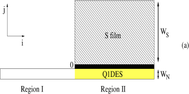
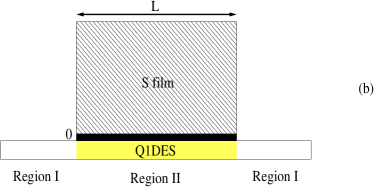
In this section we study the density of states (DOS) in a quasi-one-dimensional electron system (Q1DES) coupled in parallel to a superconducting film via an interfacial barrier. We consider the two geometries shown in Figs. 1(a) and (b). The heterostructures are assumed two-dimensional and located in the plane . Our results can be easily extended to an out-of-plane periodic structure defining a quasi-two-dimensional electron system on the normal side.
II.1 Description of the method
To analyze the superconducting proximity effect in the Q1DES we employ a numerical approach to solve the Bogolubov-de Gennes (BdG) equation
| (7) |
for the electron and hole wavefunctions. The method allows for performing a straight-forward discretisation on a real-space grid of the one-particle Hamiltonian , the pairing potential , and the potential (to be defined later). and are the chemical potential and the electron mass, both constant throughout the entire system. No translational invariance in the -direction is invoked so that studies of the structures in Figs. 1(a) and (b) are possible.
The discretized BdG equations read
| (8) | |||
where and refer to sites on a two-dimensional lattice in the and directions, respectively, and primes denote summation over nearest neighbours. The origin of the coordinate frame is indicated in Figs. 1(a) and 1(b) by the zero. If required, Eq. (8) can be generalized to a position dependent effective mass for specific materials PRB84MB .
The parameters of the numerical scheme are as follows. The potential is infinite everywhere outside the N and S systems. For every within the materials, for and otherwise. A positive potential step accounts for the fact that the coupling to the superconductor may result in a slight reduction of the Fermi energy of the Q1DES in region (II) in Figs. 1(a) and 1(b) compared to that in the uncoupled region (I) (cf Ref. Weiss, ). This turns out to be important when considering scattering of quasiparticles incident at region (II), which is analyzed in the next section. The pairing potential in Eq. (8) is assumed position-independent and equal to (s-wave) in the superconductor and zero everywhere else. Although the self-consistency is ignored, the stepwise order parameter has proved to be a satisfactory approximation for studying the proximity effect in clean systems Been ; Lambert . The absolute value of is inverse proportional to the mesh parameter , which is varied until convergence of the results is reached. A sufficient condition is , where is the superconducting coherence length and () is the Fermi wavelength (velocity). To simulate the effect of a relatively thick superconducting film, we consider for the spectral properties and for the results of Section III. Increasing this ratio does not have any quantitative effect at . In particular, all features discussed below are already observed for but with prominent finite-size effects for high quasiparticle energies . The width of the normal region is fixed to , allowing only one propagating mode along the Q1DES. The ratio is chosen to be 2 (see also endnote ratio, ).
A tunneling barrier at the N/S interface (dark area in Fig. 1) is introduced via an effective Hamiltonian equivalent to adding
| (9) | |||
to Eq. (8) for every within region (II). Essentially, the above boundary conditions define the coupling between the normal and the superconducting systems via the interfacial constant . The latter may arise from a formal procedure JMP62L that projects out the degrees of freedom within an insulating layer with a very high barrier, when neglecting the energy and momentum dependence of the penetration length. In what follows, we express all energies in units of for convenience.
To calculate the DOS of the hybrid N/S system (region (II) in Fig. 1) and, later, to study the scattering and transport properties of quasiparticles incoming from normal region (I), we use a volatile numerical method used in studies of the magnetoresistance of hybrid systems PRB99TSL ; PRB99SLJ , phonon transport PRB04FKL , and more recently in molecular electronics CPL04FKE . It is based on recursive Green function techniques. Although some of the implementation details may differ TIMES , the main stages of the computational scheme are explained in Ref. PRB99SLJ, .
II.2 Quasiparticle density of states
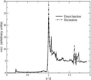
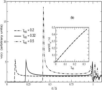
The proximity effect is reflected in the DOS, , of the hybrid system plotted in Fig. 2 for and . The solid line corresponds to the semi-infinite geometry shown in Fig. 1(a). In this case is calculated from the Green function of region (II) via the well-known relation , where the summation is over all lattice sites in the hybrid part of the junction; the factor normalises the area under the curve to a reference unit and means the imaginary part. The dashed line corresponds to the geometry of Fig. 1(b) for a relatively long wire . In this case, we obtain using a recursive technique (negative-factor counting Mark ) that allows one to calculate the effective (renormalised) interaction between the normal leads JMP62L by projecting out the degrees of freedom of the middle region (II).
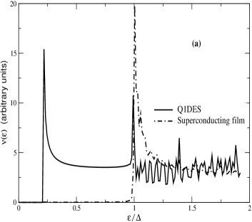
Both approaches reveal the formation of a two-gap structure: a smaller gap (minigap) at and the usual BCS singularity at with a finite quasiparticle contribution at intermediate energies, . Figure 3(a) shows the DOS separately for the Q1DES (solid line) and for the superconductor (dashed line) from which one can conclude that the smaller gap opens in the DOS of the Q1DES. This observation along with the dependence of on the coupling to the superconductor shown in Fig. 3(b) suggests that the minigap formation is a signature of the superconducting correlations induced in the Q1DES. They are maintained in the course of multiple Andreev reflections in the channel which mix particle and hole states with energies below the effective pairing energy coinciding with MiniTh . At higher energies the electrons and holes in the Q1DES are weakly correlated and hence can be treated as one-particle excitations.
In mesoscopically large diffusive N/S systems the formation of the minigap has been studied in a number of theoretical papers (see, e.g, Refs. Golubov, ; Belzig, ; Altland, ). In the clean limit, the minigap structure has been analyzed to some extent in billiard geometries resembling quantum dots Billiards ; Ihra ; Cserti .
Below we develop an analytical model, close in spirit to our numerical approach, that provides a simple description of the superconducting correlations in ballistic wires based on a 1D BdG-like equation with an effective proximity-induced pairing energy .
II.3 Proximity effect in a clean quantum wire: An analytical model
Although the physical mechanism responsible for the minigap formation in ballistic 2D electron systems has been explored in Ref. MiniTh, , the proposed method of derivation of heavily relies on the following assumptions. Firstly, the pairing potential in the superconductor was assumed homogeneous. Secondly, a finite-thickness normal system was modelled by a rectangular confining potential enabling a plane wave description of the multiple reflection in the normal channel. The advantage of the model of Ref. MiniTh, is that it allows one to obtain the minigap for an arbitrary interfacial transparency. In this subsection we present an alternative microscopic derivation of that does not rely on any particular models for and , but is restricted to low interfacial transparencies and low energies . By focusing on this case (weak-coupling regime) we would like to emphasize that the effects related to the minigap formation can be observed even in samples with average interfacial quality provided that the temperature is low enough. As in Ref. MiniTh, , we also assume the translational invariance along the N/S interface and different Fermi energies and Fermi momenta on the S and N sides.
It is convenient to rewrite the BdG equation (7) for the two-component wavefunction in the superconductor () in a more compact form:
| (10) |
Here, is the momentum parallel to the interface; and are the Pauli and unity matrices, respectively. In the normal system () the equation for is
| (11) |
with . The confining potential defines a Q1D channel with a localized electron wavefunction in the -direction.
The interfacial barrier is assumed rectangular with the electron penetration length determined by the barrier height measured from the Fermi energy. Inside a high enough barrier one can neglect the energy and momentum dependence of the penetration length and write the BdG equation as where is the barrier thickness. We introduce a special notation for the BdG wavefunction inside the barrier to distinguish it from that outside the barrier. The continuity of the particle current imposes usual boundary conditions at the barrier walls, reading
| (12) | |||
| (13) |
The solution inside the barrier satisfying the boundary condition (12) is Inserting it into the boundary conditions (13) for the derivatives, we have:
| (14) | |||
| (15) |
where and . Equations (14) and (15) serve now as effective boundary conditions for the BdG equations in the superconductor and the normal system. In the limit , the coupling between the ”normal” and the ”superconducting” functions vanishes, which is described by Eqs. (14) and (15) with zero right-hand sides.
We use boundary conditions (14) and (15) to describe Andreev reflection at the superconductor-Q1DES interface under the assumption that the influence of the Q1DES on the superconductor can be neglected. To proceed, it is convenient to include the boundary condition (15) into the BdG equation (10) by introducing appropriate delta-function terms as follows
| (16) |
We note that the admitted singular potential reproduces Eq. 15 with zero right-hand side (”isolated superconductor”).
The penetration of Andreev bound states into the superconductor at low energies is described by a particular solution of Eq. (16) generated by the right-hand side containing the ”normal” function . It can be expressed in terms of the matrix Green function of Eq. (16) whose matrix elements are constructed from the quasiparticle and condensate (Gorkov’s) Green functions, namely,
| (19) |
Here the Green functions satisfy boundary condition (15) with zero right-hand side. Inserting this solution into the boundary condition (14) at the ”normal” side and neglecting both energy and momentum dependence of the Green functions under conditions and , one finds
| (20) |
where is the condensate Green function taken at the boundary of the superconductor. We have omitted the terms proportional to since for they would only result in a shift of the dispersion.
The right-hand side of the boundary condition (20), which is off-diagonal in the particle-hole space, takes into account the conversion of a particle into a hole (and vice versa) due to Andreev reflection, that occurs simultaneously with normal scattering. In a narrow quantum wire, whose thickness is of order of the Fermi wavelength, the anomalous term in the boundary condition (20) gives rise to an effective pairing energy between particles and holes in the wire. Indeed, combining the equation of motion (11) and the boundary condition (20), one can write
| (21) |
where the singular potential is equivalent to the boundary condition (20) with zero right-hand side. For a weakly coupled Q1DES, the spatial dependence of the BdG function is almost unaffected by tunneling. Therefore, multiplying Eq. 21 by and integrating over , one obtains the following one-dimensional equation:
| (22) | |||
| (23) |
plays the role of the effective singlet pairing energy in the wire; denotes the Fermi momentum in the Q1DES.
According to Eq. (22), the excitation spectrum in the Q1DES is with the Fermi velocity . It has an energy gap given by Eq. (23) and, hence, the DOS of the normal system displays a BCS-like singularity at . To estimate , one can use the condensate Green function of a superconductor with a homogeneous pairing potential at zero energy and parallel momentum, , where . The integration over gives . The boundary value of the transverse function can be estimated using the unperturbed boundary condition , where on the right-hand side one can use the ”hard wall” wavefunction , which gives . Thus, the effective pairing energy is
| (24) |
with being the energy of the lowest occupied subband in the quantum well. Equation (24) is equivalent to the one obtained in Ref. MiniTh, for a strong delta-shaped barrier.
Equation (23) for the minigap provides a link to the numerical approach and results discussed earlier. According to Eq. (23), the size of the minigap depends on the parameter that characterizes ”hopping” between the systems (see Eq. (19)). This parameter represents a direct analogue of the coupling constant that determines the size of the minigap in the DOS in our numerical study [see Fig. 3(b)]. Since is quadratic in , the numerical value of the minigap should scale with as
| (25) |
which can indeed be verified numerically (see inset in Fig. 3(b)). In the next section we will see that the parabolic dependence of the effective pairing energy (25) on can also be extracted from calculations of the Andreev scattering probability.
III Quasiparticle scattering: length and energy dependence
In this section we discuss electron scattering properties that can be used as an independent and more complete probe of the proximity effect in finite length parallel N/S contacts. For definiteness we consider particles in the left region (I) of Fig. 1 propagating to the right. When incident at the boundary with the proximity region, these may be: (a) Andreev reflected, namely, converted into outgoing holes with the probability , (b) normally reflected as outgoing particles, i.e., without Andreev conversion, with the probability , and (c) normally transmitted as particles with the probability either in the region (II) of Fig. 1(a) or in the right region (I) of Fig. 1(b). Finally, the probability of being Andreev transmitted to the right is determined via particle conservation, namely, . In our calculations, this is ensured by the unitarity of the scattering matrix.
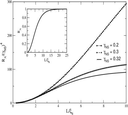
We examine first the dependence of the zero-energy Andreev reflection coefficient on the length of the proximity region (II) in Fig. 1(b) for different values of the coupling parameter and without any potential mismatch at the (I)/(II) boundary (). In conventional N/S/N structures the Andreev coefficient is known to scale as for much shorter than the coherence length PRB95CHL . According to the results of the previous section, in our case the effective pairing energy [Eq. (23)] should act as and therefore we expect that or, according to Eq. 25, for short enough contacts. This scaling is demonstrated in Fig. 4 by the convergence of the appropriately normalized curves and their parabolic shape at short lengths. As shown in the inset, there is a characteristic length beyond which the Andreev probability approaches its unit limit. Moreover, the ratio of coincides with the ratio of the gaps found from the analysis of the DOS in the previous section:
| (26) |
The overall length dependence implies that the reflectionless tunneling builds up due to the strong mixing of particles and holes in long channels. In particular, the semiclassical approaches of Ref. vanWees, and Imry, interpret reflectionless tunneling in terms of the increase in the cumulative Andreev reflection probability with increasing number of single Andreev reflections at the N/S boundary in the limiting case of an infinitely long interface .
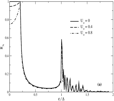
We now turn to the discussion of scattering of finite-energy quasiparticles in the semi-infinite geometry of the proximity region [Fig. 1(a)] where the reflectionless tunneling is most pronounced. We also take into account a finite potential step at the boundary between the normal (I) and proximity (II) regions that, as has been already mentioned, may arise from the modification of the Fermi energy in region (II) due to the coupling to the superconductor. The energy dependence of the Andreev reflection coefficient is plotted in Fig. 5(a) for various and . At low energies the shape of the dependence resembles that of high-transparency N/S point contacts discussed by Blonder, Tinkham and Klapwijk (BTK) BTK . If there is no potential step between the normal (I) and proximity (II) regions, the probability equals unity and starts to drop at . For , finite normal reflection builds up (shown in Fig. 6(a)) which results in smaller zero-energy values of . The appearance of the second narrow peak at comment1 manifests the crossover from the reflectionless tunneling regime, which involves a two-particle process, to the usual independent electron tunneling through the barrier.
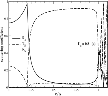
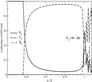
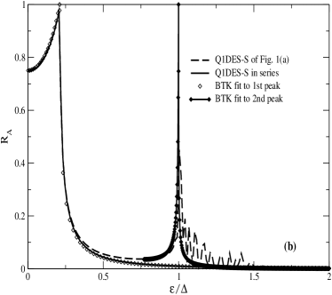
In Fig. 5(b) we demonstrate that the low- and high-energy peaks in the dependence of can be independently fitted by the BTK model BTK . To fit the low-energy behaviour we use the formulas of Table II in Ref. BTK, with and a small barrier parameter . For the tunneling peak we use the same formulas with and the large barrier parameter . In either of the above limiting cases, the fit is almost perfect. To describe the crossover between them, a more general analytical model is needed.
In Fig. 6 all non-vanishing scattering coefficients are plotted for: (a) and (b) no barrier between the normal (I) and proximity (II) regions. For there is normal reflection of particles at the (I)/(II) interface caused by the potential mismatch. For it vanishes not only below the minigap but also at the intermediate energies . This is due to the specific geometry of our tunnel junction where quasiparticles with intermediate energies are mainly transmitted through the channel experiencing low-probability Andreev reflection (cf the behaviour of and ). At higher energies , when the superconductor becomes transparent for quasiparticles, the lack of the translational invariance of our system causes considerable normal scattering and oscillations of all the coefficients due to the finite thickness of the superconductor.
IV Concluding remarks
Scattering coefficients are related to the two-, three-, and in general multi- probe conductances of N/S systems (see, e.g., Refs. BTK, , Lambert, ). Therefore, the proximity effect discussed in the previous section should be observable in measurements of the current-voltage characteristics of such hybrids. In order to explore this possibility and to elaborate on our discussion of the experimental reports Morpurgo ; Kroemer ; Weiss ; Rahman , we conclude by focusing on the two-probe differential conductance of the semi-infinite geometry of Fig. 1(a). This is given by Lambert
| (27) |
where with () for (p)articles and () for (h)oles. The bias energy is introduced as the difference between the chemical potentials in the normal region and in the hybrid part of the junction, with the latter taken as reference.
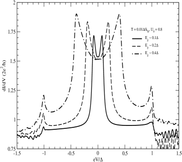
At zero-temperature, Eq. (27) reduces to . Hence, for a small barrier between the normal (I) and proximity (II) regions of the wire, the dependence of at ultralow reflects mainly the energy dependence of the Andreev probability [Fig. 5(a)]. The same is true for the length dependence of the zero-bias conductance. In Fig. 7 we plot the differential conductance for several values of interfacial coupling (i.e., ) at . Unlike the tunneling peaks at , the proximity-induced anomalies at the minigap energy exhibit a strong dependence on (cf Fig. 3(b)).
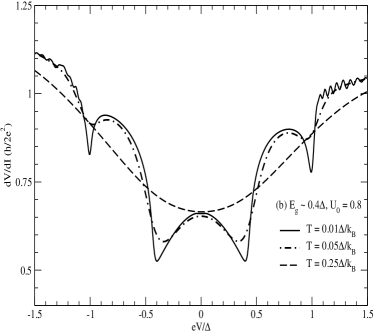
In Fig. 8, the evolution of the differential resistance, which is defined as the inverse of Eq. 27, is shown as a function of temperature. At intermediate , features at the scale of the minigap are smeared and the resistance exhibits an overall dip as a result of the reflectionless tunnelling. With decreasing the temperature to the resistance curve develops a finer structure reflecting the energy dependence of the Andreev reflection probability. For vanishing potential step (Fig. 8(a)), there are two minima symmetric to zero bias at the energies of the superconducting gap. In addition to those, for (Fig. 8(b)) the finite normal reflection at leads to a zero-bias resistance peak superimposed on the Andreev dip.
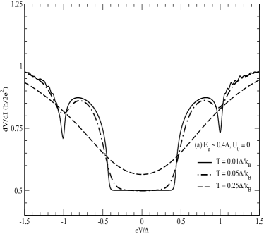
According to Fig. 4, for pronounced Andreev reflection the contact length must be of order of the proximity-induced coherence length . For typical for Nb electrods, can be estimated as . On the other hand, in the device of Ref. Morpurgo, the contact overlap between the nanotube and the superconductor was rather large, about . Therefore, the condition could be met leading to the observed zero-bias reduction of the contact resistance. Another feature of our curves, namely the appearance of a small zero-bias peak superimposed on the Andreev dip due to finite normal scattering at very low (Fig. 8(b)), is also consistent with the experimental findings.
We note that in the experiment of Ref. Morpurgo, the low-bias behaviour of the resistance was sensitive to a gate voltage applied to the carbon nanotube. In our model the effect of the gate voltage can be incorporated into the difference between the Fermi energies in the normal (I) and proximity (II) regions in Fig. 1. We have focused on the most interesting case of relatively small when normal scattering does not impede the conversion of the quasiparticle current into the supercurrent in the proximity region. As increases, the low-bias resistance dip in Fig. 8(b) eventually evolves into an overall peak above the normal state value like in non-ideal N/S point contacts BTK ; PRBNFJ99 .
We emphasize that the zero-bias anomaly discussed here is a property of a single parallel N/S contact. Although as argued in Ref. Morpurgo, in their S/CN/S devices the two CN/S interfaces acted independently, the role of the interelectrode coupling remains unclear. Such a question has been investigated numerically in Ref. Wei, for a somewhat simpler system where a carbon nanotube is connected to a normal metal and a superconductor via tunnel barriers (N/CN/S). It was shown that resonant tunneling through Andreev levels in the nanotube can significantly increase the low-bias subgap conductance similar to the situation in mesoscopic N/quantum dot/S structures Been . For a comprehensive theory of transport in S/CN/S hybrids this aspect together with the contact geometry and electron interaction effects must be taken into account. In addition, one should bear in mind that in the experimental realizations a number of CNs have been contacted in parallel.
In Refs. Kroemer, and Weiss, a strong zero-bias suppression of the resistance was found in ballistic 2D electron systems in extended planar coupling to superconductors at . These systems can be considered as a generalization of that shown in Fig. 1. For perfect planar interfaces, individual channels with possibly different barriers and interfacial transparencies PRBNFJ99 add up independently. However, interchannel mixing must be considered for rough surfaces. The same applies when considering experiments in quantum wires Rahman with few propagating modes. It is worth noting that in this case the behaviour similar to the low- differential conductance of Fig. 7 was observed. We believe that the transport anomalies observed in 1D Morpurgo , quasi-1D Rahman and 2D Kroemer ; Weiss systems have a contribution of a common nature stemming from the proximity-induced mixing of particles and holes which mediate the conversion of a normal current into a supercurrent along the contact on the scale of the coherence length and at energies smaller than the minigap .
Acknowledgements.
We thank A.F. Morpurgo for communicating the geometrical parameters of S/CN/S structures studied in Ref. Morpurgo, . GF acknowledges funding by the ATOM CAD project within the Sixth Framework Programme of the EU and by the Science Foundation Ireland. This work was also supported by the Deutsche Forschungsgemeinschaft (Forschergruppe 370, Graduiertenkolleg 638).References
- (1) R. Fazio, F.W.J. Hekking, and A.A. Odintsov, Phys. Rev. Lett. 74, 1843 (1995); C. Winkelholz, R. Fazio, F.W.J. Hekking, and G. Schön, Phys. Rev. Lett. 77, 3200 (1996).
- (2) D.L. Maslov, M. Stone, P.M. Goldbart, and D. Loss, Phys. Rev. B 53, 1548-1557 (1996).
- (3) Y. Takane, J. Phys. Soc. Jpn. 66, 537 (1997).
- (4) I. Affleck, J.-S. Caux, and A.M. Zagoskin, Phys. Rev. B 62, 1433 (2000).
- (5) Y. Wei, J. Wang, H. Guo, H. Mehrez, and C. Roland, Phys. Rev. B 63, 195412 (2001).
- (6) M. Titov, N.A. Mortensen, H. Schomerus, and C.W.J. Beenakker, Phys. Rev. B 64, 134206 (2001).
- (7) J. Gonzalez, Phys. Rev. Lett. 87, 136401 (2001); J. Phys.: Condens. Matter 15, S2473 (2003).
- (8) S. Vishveshwara, C. Bena, L. Balents, and M.P.A. Fisher, Phys. Rev. B 66, 165411 (2002).
- (9) B.K. Nikolic, J.K. Freericks, and P. Miller, Phys. Rev. Lett. 88, 077002 (2002).
- (10) H.-W. Lee, Hyun C. Lee, Hangmo Yi, and Han-Yong Choi, Phys. Rev. Lett. 90, 247001 (2003).
- (11) J. Jiang, L. Yang, J. Dong, and D.Y. Xing, Phys. Rev. B 68, 054519 (2003).
- (12) E. Vecino, A. Martín-Rodero, and A.L. Yeyati, Phys. Rev. B 68, 035105 (2003).
- (13) Y. Tanaka, A.A. Golubov, and S. Kashiwaya Phys. Rev. B 68, 054513 (2003).
- (14) A.Yu. Kasumov, R. DeBlock, M. Kociak, B. Reulet, H. Bouchiat, I.I. Khodos, Yu.B. Gorbatov, V.T. Volkov, C. Journet, and M. Burghard, Science 84, 1508 (1999); A. Kasumov, M. Kociak, M. Ferrier, R. DeBlock, S. Gueron, B. Reulet, I. Khodos, O. Stephan, and H. Bouchiat, Phys. Rev. B 68, 214521 (2003).
- (15) A.F. Morpurgo, J. Kong, C.M. Marcus, and H. Dai, Science 286, 263 (1999); Physica B 280 382 (2000).
- (16) M.R. Buitelaar, T. Nussbaumer, and C. Schönenberger, Phys. Rev. Lett. 89, 256801 (2002).
- (17) J. Haruyama, K. Takazawa, S. Miyadai, A. Takeda, N. Hori, I. Takesue, Y. Kanda, N. Sugiyama, T. Akazaki, and H. Takayanagi, Phys. Rev. B 68, 165420 (2003); J. Haruyama, A. Tokita, N. Kobayashi, M. Nomura, S. Miyadai, K. Takazawa, A. Takeda, and Y. Kanda, Appl. Phys. Lett. 84, 4714 (2004).
- (18) M. Bockrath, D.H. Cobden, J. Lu, A.G. Rinzler, R.E. Smalley, L. Balents, and P.L. McEuen, Nature 397, 598 (1999).
- (19) M.S. Dresselhaus, G. Dresselhaus, and P.C. Eklund, Science of Fullerenes and Carbon Nanotubes (Academic, San Diego, 1996).
- (20) A.F. Andreev, Zh. Exp. Teor. Fiz. 46, 1823 (1964) [Sov. Phys. JETP 19, 1228 (1964)].
- (21) G.E. Blonder, M. Tinkham, and T.M. Klapwijk, Phys. Rev. B 25, 4515 (1982).
- (22) C. Nguyen, H. Kroemer, and E.L. Hu, Phys. Rev. Lett. 69, 2847 (1992).
- (23) F. Rahman and T.J. Thornton, Superlat. Microstr., 25 767 (1999).
- (24) J. Eroms, M. Tolkiehn, D. Weiss, U. Rössler, J. DeBoeck, S. Borghs, Europhys. Lett. 58, 569 (2002); J. Eroms, PhD thesis, Universität Regensburg, 2002.
- (25) A.F. Volkov, P.H.C. Magnee, B.J. van Wees, and T.M. Klapwijk, Physica C 242, 261 (1995).
- (26) A. Kastalsky, A.W. Kleinsasser, L.H. Greene, R. Bhat, F.P. Milliken and J. P. Harbison, Phys. Rev. Lett. 67, 3026 (1991).
- (27) B.J. van Wees, P. de Vries, P. Magnee, and T.M. Klapwijk, Phys. Rev. Lett. 69, 510-513 (1992).
- (28) A.F. Volkov, Phys. Lett. A 174, 144 (1993); A.F. Volkov, A.V. Zaitsev, and T.M. Klapwijk, Physica C 210, 21 (1993).
- (29) C.W.J. Beenakker, Phys. Rev. B 46, R12841 (1992); Rev. Mod. Phys. 69, 731 (1997).
- (30) I.K. Marmorkos, C.W.J. Beenakker, and R.A. Jalabert Phys. Rev. B 48, R2811 (1993).
- (31) J. Nitta, T. Akazaki, and H. Takayanagi, Phys. Rev. B 49 R3659 (1994).
- (32) W. Poirier, D. Mailly, and M. Sanquer, Phys. Rev. Lett. 79, 2105 (1997).
- (33) C.J. Lambert and R. Raimondi, J. Phys: Condens. Matter 10, 901 (1998).
- (34) G.B. Lesovik, A.L. Fauchere, and G. Blatter, Phys. Rev. B 55, 3146 (1997).
- (35) M. Schechter, Y. Imry, and Y. Levinson, Phys. Rev. B 64, 224513 (2001).
- (36) I.E. Batov, Th. Schäpers, A.A. Golubov, and A.V. Ustinov, J. Appl. Phys. 96, 3366 (2004).
- (37) D. Ferry and S.M. Goodnick, Transport in Nanostructures (Cambridge University Press, Cambridge, 2000)
- (38) V.T. Petrashov, V.N. Antonov, P. Delsing, and T. Claeson, Phys. Rev. Lett. 74, 5268-5271 (1995); W. Belzig, R. Shaikhaidarov, V.V. Petrashov, and Yu.V. Nazarov, Phys. Rev. B 66, 220505(R) (2002).
- (39) H. Courtois, Ph. Gandit, D. Mailly, and B. Pannetier, Phys. Rev. Lett. 76, 130-133 (1996); P. Dubos, H. Courtois, O. Buisson, and B. Pannetier, ibid. 87, 206801 (2001).
- (40) A.A. Golubov, E.P. Houwman, J.G. Gijsbertsen, V.M. Krasnov, J. Flokstra, H. Rogalla, and M.Yu. Kupriyanov, Phys. Rev. B 51, 1073 (1995); B.A. Aminov, A.A. Golubov, and M.Yu. Kupriyanov, Phys. Rev. B 53, 365 (1996).
- (41) W. Belzig, C. Bruder, and G. Schön, Phys. Rev. B 54, 9443 (1996).
- (42) A. Kadigrobov, L.Y. Gorelik, R.I. Shekhter, M. Jonson, R.Sh. Shaikhaidarov, V.T. Petrashov, P. Delsing, and T. Claeson, Phys. Rev. B 60, 14589 (1999).
- (43) A. Altland, B.D. Simons, and D. Taras-Semchuk, Adv. Phys. 49, 321 (2000).
- (44) A. Anthore, H. Pothier, and D. Esteve, Phys. Rev. Lett. 90 (2003) 127001.
- (45) J.A. Melsen, P.W. Brouwer, K.M. Frahm, and C.W.J. Beenakker, Europhys. Lett. 35, 7 (1996); H. Schomerus and C.W.J. Beenakker, Phys. Rev. Lett. 82, 2951 (1999); P. Jacquod, H. Schomerus, and C.W.J. Beenakker, Phys. Rev. Lett. 90, 207004 (2003).
- (46) W. Ihra, M. Leadbeater, J.L. Vega, and K. Richter, Euro. Phys. J. B. 21, 425 (2001).
- (47) J. Cserti, A. Kormányos, Z. Kaufmann, J. Koltai, and C.J. Lambert, Phys. Rev. Lett. 89, 057001 (2002); J. Cserti, P. Polinak, G. Palla, U. Zülicke, and C. J. Lambert Phys. Rev. B 69, 134514 (2004).
- (48) R.A. Morrow and K.R. Brownstein, Phys. Rev. B 30, 678 (1984).
- (49) Although in real superconducting materials, the actual value of this ratio does not affect our results other than increasing significantly the computational cost if made much greater than unity.
- (50) P-O. Löwdin, J. Math. Phys. 3, 969 (1962).
- (51) F. Taddei, S. Sanvito, and C.J. Lambert, Phys. Rev. B 63, 012404 (2001).
- (52) S. Sanvito, C.J. Lambert, J.H. Jefferson, and A.M. Bratkovsky, Phys. Rev. B 59, 11936 (1999).
- (53) G. Fagas, A.G. Kozorezov, C.J. Lambert et al, Phys. Rev. B 60, 6459 (1999).
- (54) G. Fagas, A. Kambili, and M. Elstner, Chem. Phys. Lett. 389, 268 (2004).
- (55) We use an optimised F90 implementation developed by one of the authors (GF). It is generalised to include manipulation of non-orthogonal matrices, needed to tackle arbitrary geometries, and of possible non-orthogonal basis sets for applications to materials.
- (56) M. Leadbeater, PhD Thesis, Lancaster University, 1996.
- (57) N.R. Claughton, V.C. Hui, and C.J. Lambert, Phys. Rev. B 51, 11635 (1995).
- (58) We have checked that approaches unity at both the minigap (when ) and superconducting gap energies for selected cases. This requires a fine choice of the energy grid due to the singular behaviour of the peaks and, hence, increased computational time. Since our results do not depend crucially on this, this practice has been avoided.
- (59) N.A. Mortensen, K. Flensberg, and A.-P. Jauho, Phys. Rev. B 59, 10176 (1999)