Solid immersion lens–enhanced micro–photoluminescence: principle and applications
Abstract
We demonstrate the combination of a hemispherical solid immersion lens with a micro–photoluminescence set–up. Two advantages introduced by the SIL, an improved resolution of 0.4 times the wavelength in vacuum and a 5 times enhancement of the collection efficiency, make it an ideal system for spatially resolved spectroscopy applications. The influence of the air gap between the SIL and the sample surface is investigated in detail. We confirm the tolerance of the set–up to an air gap of several micrometers. Such a system is proven to be ideal system in the studies of exciton transport and polarization dependent single quantum dot spectroscopy.
I Introduction
Photoluminescence (PL) is one of the most important methods to investigate electronic states in semiconductors. Since semiconductor nanostructure becomes increasingly important in optoelectronic applications, the PL has been developed to local spectroscopy. To realize spatial resolution, one needs local excitation or local detection or both. In far–field optics, the resolution is limited by diffraction. In a common micro-photoluminescence (-PL) system, the achieved resolution is about 1 m. This limitation of the resolution can be overcome by working in the near–field regime, where the diffraction limit is not yet established. Scanning near-field optical microscopy (SNOM), designed according to this idea, realized a resolution of 100 nm. Despite of this high resolution, several inherent as well as technical problemsapl1791 limit the performance of SNOM.
Another way to deal with the diffraction limitation is to increase the refractive index of the media around the sample, i.e., to increase the effective numerical aperture () of the optical system. This can be realized by immersing the sample into oil or put a tiny lens, named solid immersion lens (SIL), on the surface of the sample. In the case of semiconductor spectroscopy, the latter is more suitable since SIL is easily to be dealt with and there is no risk to contaminate the sample.
During the last decade, SIL has been used in solid immersion microscopeapl2615 and (magneto–)optical data storageapl388 for high spatial resolution or high storage density, respectively. Recently, SIL has also been introduced in spatially resolved pump–probe experiments.apl1791 ; jm194523 . By including a superspherical SILbokborn (s–SIL) in a –PL system, an improved spatial resolution at room temperaturejjapl962 as well as low temperaturesapl635 has been demonstrated by PL imaging measurements of GaAs quantum well (QW). The high spatial resolution has allowed to study carrier migration under globalapl635 or localapl2965 excitation conditions. Besides, s–SIL has also been used in a scanning –PL setup to investigate exciton localization in GaAs QW prl2652 ; pssb505 .
Up to now, only s–SIL has been applied in –PL system. But, the thickness of an s–SIL is designed for one particular wavelength since the incident parallel beam is focused at the distance away from the top of the s–SIL, where is the radius of the SIL and is the refractive index of the SIL material. Consequently, the focus of an s–SIL is wavelength-dependent since depends on the wavelength of light, . On the contrast, a hemispherical SIL (h–SIL) is universal for any wavelength. In a PL experiment, one typically deals with different wavelengths for excitation and detection. Thus, although an s-SIL can improve the resolution times while an h-SIL can only improve it times, the latter is more appropriate for PL studies.
In this paper, we demonstrate for the first time the combination of an h-SIL with a confocal -PL system. We confirm the realized spatial resolution of by introducing the h-SIL. We also find an enhancement of collection efficiency of about 5 times, which is consistence with a theoretical estimation. We discuss in detail the influences of an air gap between the SIL and the sample surface on the resolution and collection efficiency. We demonstrate that an air gap of several micrometers can be tolerated in a system with . Finally, some applications of this system to semiconductor spectroscopy are discussed, with an emphasis on its advantages over a SNOM system.
II Solid immersion lens–enhanced micro–photolumine-scence
II.1 Experimental Setup
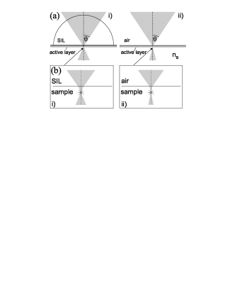
Figure 1 shows schematically the SIL–enhanced –PL system. The excitation source can be a continuous wave (cw) or pulse laser. The laser beam is expanded to fit the diameter of objective, then reflected by a beam–splitter and focused on the sample surface through a microscope objective (20 , numerical aperture ). The same objective is used for collecting the PL from the sample. The signal passes the beam-splitter and a tube lens and is then focused to the image plane of the microscope. A set of pinholes, with different sizes, is installed in the image plane to select the detection area. By scanning the pinhole in the image plane, one can detect luminescence from different positions on the sample surface. For cw measurements, the PL is recorded by a double-grating monochromator and a cooled CCD camera, with a spectral resolution of 30 eV. For time–resolved measurements, a streak camera with temporal resolution of 2 ps is used in combination with a CCD camera with photon counting.
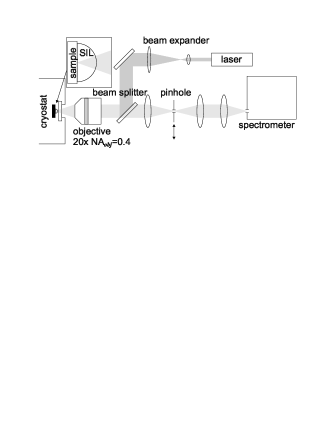
The h–SIL, made of Zr with at nm, is adhesively fixed to the sample surface. The sample with the SIL is vertically mounted in a helium–flow cryostat. The SIL can be used in the temperature range of 6300 K for an unlimited number of cooling cycles. The diameter of the SIL is chosen to be 1 mm, which is large enough for giving an enough working area for spectroscopy and being handled without any special equipment, and still small enough to be sticked on the sample adhesively even in vertical configuration.
II.2 Spatial Resolution
In a far–field optical system, the spatial resolution is limited by diffraction of the light. For a plane wave incident light, the half width at half maximum (HWHM) of the Airy pattern is given by
| (1) |
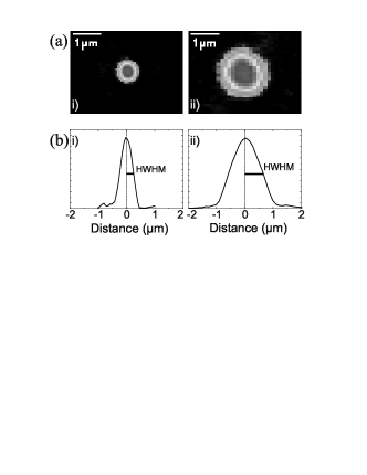
Here, represents the refraction index of the media around the sample. Without SIL, (air) and with the h–SIL we have . Thus, by introducing the h–SIL, we can improve the resolution by more than 2 times. In order to confirm the achieved resolution, we install the SIL onto an arbitrary flat sample and focus the incident laser beam of a He–Ne laser on the sample surface (i)underneath and (ii)outside the SIL, respectively. We measure two–dimensional intensity maps of the laser spots in both case, as shown in Fig. 2(a) with the same color encoding. The length–scale collaboration in these maps is obtained by imaging an optical grating with known parameters. The spatial intensity profiles in Fig. 2(b) are obtained by taking a line–scan across the laser spots. As expected, the profile with SIL (i) is about 2 times narrower than that obtained without SIL (ii). In (i) the realized spatial resolution (HWHM of the laser spot) is (corresponding to 260 nm for the He–Ne laser (633 nm)) in contrast to for (ii). We note that the achieved values of HWHM in both cases are larger than that calculated from Eq. 1. This is consistent with theoretical calculationprsl358 , and can be attributed to the Guassian profile, rather than plane wave, of the laser beamrpp427 used in the experiment and the high NAprsl358 of the system.
In a confocal -PL system, the resolution can be further improved by introducing a pinhole with a suitable size to the image plane of the microscope.rpp427 In the followings, we present a quantitative analysis of this further improvement. The illumination function of the laser excitation can be described by a Guassian function,
| (2) |
Here, is the coordinate in the focal plane, i.e., sample surface, and is the spot radius at . The detection function can also be described by Guassian function, but with a different radius since generally the wavelength of the luminescence is different from that of the excitation laser in a PL experiment. The transmission function of the pinhole is
| (3) |
with the radius of the pinhole image. Thus, the detection probability, i.e., the probability of a photon emitted at point transmit the pinhole thus be detected, is given by
| (4) |
The confocal acceptance function (CAF) is then given by
| (5) |
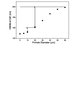
Based on the above analysis, we calculate the of our SIL–enhanced –PL system. Figure 3 shows the calculated HWHM of the CAF, which defines the confocal resolution, as function of the pinhole size. The horizontal line represents the resolution obtained without pinhole. We find that a pinhole of 60 m has no effect on the resolution, but decreasing the pinhole size from that value the resolution is enhanced. Below 10 m, the enhancement is saturated while further decrease the pinhole size.
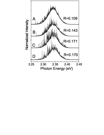
In order to confirm that the enhancement of resolution by the SIL and pinhole can be achieved in a realistic PL measurement, we measure the spectra from a ZnCdSe/ZnSe quantum dot sample with different SIL–pinhole configurations. In this sample, a ZnCdSe layer with a thickness of 2.9 monolayers is embedded between two ZnSe barriers, including Cd–rich quantum dots with an average size of about 10 nm. The spectrally sharp lines in the spectrum correspond to excitonic transitions in individual dots. The variations in size, shape and composition of these dots lead to a wide spectral distribution of the lines. Hence, in a macroscopic PL spectrum (not shown here), one observes a broad smooth emission band due to the large number of contributing dots. When decreasing the detection area, hence the number of the dots, individual sharp lines can be resolved on top of the unresolved smooth background. The resolved part becomes more and more pronounced with decreasing detection area. Eventually, once the detection area is small enough, the unresolved background will disappear. Such a kind of sample, with suitable dot density, can be used to prove qualitatively the enhancement of spatial resolution by introducing the SIL.
Figure 4 shows four spectra detected at a sample temperature of 6 K with different SIL–pinhole configurations, i.e., without SIL and pinhole (A), with SIL but without pinhole (B), with SIL and a 20 m diameter pinhole (C), with SIL and a 10 m diameter pinhole, respectively. The sample is excited by the 476.5 nm line of an Ar–ion laser. All spectra are composed of a resolved and an unresolved part, but the resolved sharp lines in the spectrum is more pronounced as we go from (A) to (D). We fit the background by a Gaussian function in order to separate the resolved and the unresolved part. The choice of a Gaussian is legitimate because of the inhomogeneous distribution of a large number of quantum dots contributing to the spectra. For each spectrum, we calculate the ratio, , of the spectrally integrated intensities of the resolved part to the unresolved smooth background. Such a ratio increases with enhancing the resolution of the system, as we discussed above. From Fig. 4 we obtain an increase of by 30 by introducing the SIL (compare 0.109 of A to 0.143 of B). By introducing a 20 m pinhole, is further increased by 20 (0.171 of C). In case D, a 10 m pinhole is used instead of the 20 m one. But we don’t find a further increase of (0.170 of D). This is consistent with our analysis discussed above. As shown in Fig. 3, the enhancement of the resolution introduced by changing a 20 m pinhole to a 10 m one (vertical dots) is much smaller than that from non–pinhole to 20 m pinhole (vertical full line). In practice, the signal level drops seriously as decreasing the pinhole size from 20 m, and the alignment becomes more difficult. Thus, a pinhole size of 20 m is the optimal choice in our system.
II.3 Collection Efficiency
In a PL experiment, only a part of luminescence from the sample can be collected due to the reflection losses and the finite size of the optics. The collection efficiency of a spectroscopy system is of crucial importance, especially in the cases of low excitation conditions or low signal level. Since it is operated in the far field, the collection efficiency of a –PL system is much higher than that of typical near–field systems. By introducing a SIL into a –PL system, the collection efficiency can be further improved. By comparing the luminescence intensities measured with SIL and without SIL, we find the enhancement of collection efficiency of our system by the SIL is about 5 times, depending mainly on the cleaning process of both the sample and the SIL.
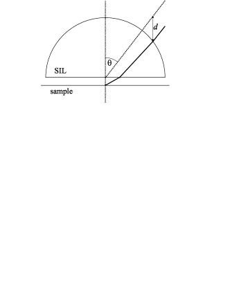
Here, we present a quantitative analysis on the enhancement of the collection efficiency introduced by using the SIL. Since the is smaller than the refraction index of the sample, , the SIL has the property to reduce the reflection losses, i.e., enhance the transmission of both the luminescence and the laser. The enhancement of the collection efficiency by this factor, , can be calculated by using Fresnel formula. Figure 5(a) shows the configurations for our calculation of the by comparing the transmissions when the SIL is used (i) or not (ii). In case (i), since the light enters perpendicularly on the top of the SIL, the transmission coefficient of the intensity is given by for all rays.
However, when entering the sample, the transmission coefficient depends of the angle of incidence and the polarization of the ray. This angle dependency is weak in the range of angles given by the microscope objective. Thus, for average, we calculate for each polarization the transmission of a ray with an angle to the optical axes of . Furthermore, the transmissions of s and p polarizations are averaged to get the total transmission. Considering the reflection losses of both the laser and the luminescence, we get an enhancement factor .
Beside this transmission enhancement, the SIL can enlarge the collection angle of the –PL system, as shown in Fig. 5(b). The solid angle outside of the sample is independent of whether the SIL is used (i) or not (ii) and is directly given by . However, the solid angle inside the sample increases when the SIL is introduced. This is due to the smaller refraction of the light at the sample surface since the material on top of the sample having now a refractive index higher than that of air. As a result, a point source emitting light in all directions as shown in Fig. 5(b) experiences a larger solid angle in which the emitted photons can be collected by the objective. A ray emitted outside of this angle will miss the objective and not contribute to the signal, even if its angle to the optical axis is smaller than the critical angle of total internal reflection. In the approximation that the photons are emitted homogeneously in all directions, the enhancement of collection efficiency due to the larger PL collection angle, , is given by the ratio of the solid angles with SIL to without SIL:
| (6) |
Thus, the total enhancement of the collection efficiency by SIL is
| (7) |
In our set–up, we have , so . This calculated value is consistent with out experimental results.
III Influence of air gap
In the analyses of the previous section, we assume that the SIL is ideally attached on the sample surface. In a realistic experiment, there exists an air gap between the flat surface of the SIL and the sample surface due to the fluctuations of both surfaces as well as due to particles between them. In this section, we discuss the influence of such an air gap on the resolution and collection efficiency of the SIL–enhanced –PL system.
As discussed above, the , of a SIL–enhanced –PL system is determined by the and , i.e., for h–SIL and for s–SIL. The influence of the air gap on the resolution depends strongly on whether or not. In a system with , near–field coupling is required. Theoretical analysis shew that even an air gap with a thickness of one fifth of the wavelength can deteriorate the resolution seriously.jap6923 In contrast, a system with is still in far–field regime, and it has been shown theoretically that an air gap of several micrometers doesn’t influence the resolution.inp56 . In our set–up, we have thus far–field coupling. To check the influence of air gap on the resolution of our system, we load the SIL on the sample with and without cleaning procedure, respectively. In the latter case, an air gap of several micrometers is anticipated (we will prove this fact later). We focus the laser beam on the sample surface, and in both cases we get the same size of the laser spots. We even load the SIL on the surface of an optical grating without any special treatment and obtain the same resolution. Thus we confirm that in a system with , an air gap of several micrometers has no influence on the resolution.
Generally, an air gap introduces additional reflection losses between the sample and the SIL, thus reduces the collection efficiency. In a near–field system with , the collection efficiency can be deteriorated seriously by an air gap of several hundreds nanometers, i.e., comparable to the light wavelength.inp56 In contrast, a system with is anticipated to be more robust due to the far–field feature. In order to investigate the tolerance of our system to the air gap, we load the SIL on a ZnCdSe/ZnSe quantum dot sample without any cleaning procedure. By comparing the spectra measured beneath or outside the SIL at a sample temperature of 6 K, we find an enhancement of collection efficiency by a factor of 2.
The explain the observed enhancement, we calculate the collection efficiency of the system with an air gap. Figure 6 shows the configuration of the SIL, air gap and the sample. As measuring the spectrum, we focus on the sample surface. The path of the ray is shown as the solid line in Fig. 6. We can also find the focus of the flat surface of the SIL, as shown as the dots. Since the images of both surfaces are clearly observable, the distance between these two foci, , can be measured accurately. In this experiment, we have =40 m. By some simple geometrical considerations, we deduce the thickness of the air gap to be 5 m from the measured . Based on Fig. 6, we calculate the collection efficiency of this configuration by the method discussed in the previous section. We obtain , so . The calculation is well consistent with the experiment. We note that the deterioration of enhancement from 5.76 to 2.36 by the 5 m air gap originates mainly from the increasing of the reflection losses ( drops from 1.2 to 0.55). The enhancement due to the enlarged collection angle, , is not sensitive to the presence of the air gap.
Thus, we prove the tolerance of the SIL–enhanced –PL system to an air gap of several micrometers. This feature is quite difference from a near–field system with . In a typical measurement, there exists an air gap of about 1 thick between the SIL and the sample surface after a regular cleaning procedure. The enhancement factor of collection efficiency is about 5 in our experiments, as mentioned above. In principle, by increasing the or , or using a s–SIL, one can further improve the resolution of a SIL–enhanced –PL system. But, if the is increased beyond 1, the near–field regime is reached, and the tolerance to the air gap drops seriously. In this sense, our choice of is a good compromise between the enhancement of spatial resolution and collection efficiency as well as the feasibility in practical operations. Further, it is worth noting that such a system can be used even for samples with rough surfaces with fluctuations of several micrometers.
IV Applications
Generally, the SIL–enhance –PL system described above can be applied to any semiconductor spectroscopy experiments whenever the spatial resolution is needed and the sample has a relative flat surface. In some cases, this system is even more suitable than any other spatially resolved methods. We present in the following two kinds of applications where the SIL–enhanced –PL system shows its unique advantages.
IV.1 Exciton Transport in Quantum Wells
The exciton in-plane transport process is an important part of exciton dynamics in QWs. Due to the continues miniaturization of electronic and optical devices thus the increasing importance of nanostructures, the transport has to be understood on a length scale comparable to the light wavelength. The resolution of a conventional –PL system, about 1 m, is not enough for this kind of studies. In SNOM, one can achieve a resolution of 100 nm by using the coated tip. But the collection efficiency is very poor. By using a uncoated tip, the collection efficiency can be improved, but simultaneously the resolution drops.apl76203 Furthermore, a SNOM experiment has another disadvantage for transport measurement: one cannot detect spatially resolved spectra from positions outside the excitation spot. Thus, one can only study the transport process indirectly.
In contrast, the SIL–enhanced –PL can be used to investigate the transport behavior in a rather direct way with sub-m resolution. By scanning the pinhole in the image plane of the objective, one can detect luminescence from positions which are different from the position where the sample is locally excited. This enables one to get the spatial profile of the luminescence intensity, thus the spatial distributions of the carrier density. The field of view of the SILinp56 (35 m in our setup) is far beyond the typical transport length of carriers. In Fig. 7, we show an example of the
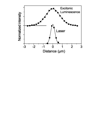
spatial profiles of the luminescence intensity measured for a ZnSe/ZnSSe multiple quantum well at 6 K. The excitation laser used for this measurement is a tunable cw Ti:Sapphire laser pumped by an Ar–ion laser and frequency–doubled using a BBO crystal. Comparing with the profile of the laser excitation spot, measured in the same pinhole–scanning, the spatial distribution of the luminescence is significantly wider due to exciton in-plane transport. The improved resolution enables us to access the hot exciton transport regime.apl801391
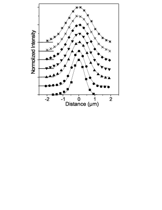
This kind of direct transport measurement can also be performed with time resolution by using a short pulse Ti:Sapphire laser and a synchroscan streak camera and CCD with photon counting. In this configuration, one can detect the time evolution of the spatial profile of luminescence, as shown in Fig. 8(b) for a ZnSe/ZnMgSSe multiple QW. The combination of the 200 nm spatial resolution with the 2 ps temporal resolution enables one to investigate more details of the exciton transport. We note that for the time-resolved measurements, the high collection efficiency introduced by the SIL is particularly crucial, not only because of the signal losses at the pinhole but also because signal intensity spread due to the time resolution.
IV.2 Single Quantum Dot Spectroscopy
Investigation on properties of individual quantum dot requires single dot spectroscopy. This can be achieved by small dot density (e.g. by nano–aperture or mesa) or high spatial resolution (e.g. SNOM). In SIL–enhanced –PL, single dot spectroscopy can also be achieved for samples with low quantum dot density. In such a system, the choice of dots is more flexible. Since there is no patterning required, it is a non–destructive method.
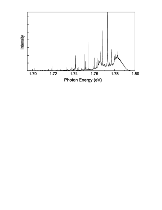
The high spatial and spectral resolutions of the SIL–enhance –PL system enable us to detect isolated narrow lines from single quantum dot undisturbed by the luminescence from other dots. Figure 9 shows a spectrum of a GaAs/AlAs superlattices. In this kind of samples, quantum dots are formed due to the interface fluctuations.s27387 . A He–Ne laser is used for excitation, with an excitation density of 0.5 W/. By using the SIL and the 20 m pinhole, isolated sharp lines from individual quantum dots are well resolved.
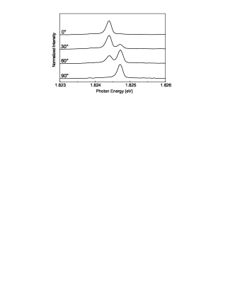
Furthermore, we confirm that the polarization information of the luminescence, which is of crucial importance e.g. in the investigations of spin dynamics, is preserved in this set–up. In Fig. 10 we show the spectra of a single quantum dot in a quantum well of 6.5 monolayers ZnCdTe embedded in ZnTe barriers. The sample is excited with the 488 nm line from the cw Ar–ion laser. To determine the polarization of luminescence, a linear polarizer is placed in the detection path. The spectra show a doublet structure composed of two lines which are linearly polarized along two orthogonal directions. Such line doublets are ascribed to fine–structure splitting of excitons in asymmetric quantum dots.jcg742 Our measurement demonstrates that SIL can be applied to -PL when the polarization of the light is of interest. It is typically very difficult to extract the polarization from other spatially resolved techniques like near-field spectroscopy.apl3929
V Summary
We demonstrate for the first time the combination of a h–SIL with a –PL set–up. Two advantages introduced by the SIL, an improved resolution of 0.4 and a 5 times enhancement of the collection efficiency, make it an ideal system for spatially resolved spectroscopy applications. We analyze the improvement of the resolution by using the pinhole, and find the optimal pinhole size. The influence of the air gap between the SIL and the sample surface is investigated in detail. We confirm the tolerance of the set–up to an air gap of several micrometers. Such a system is proven to be ideal system in the studies of exciton transport and polarization dependent single quantum dot spectroscopy.
VI Acknowledgments
We gratefully acknowledge the growth of the samples by the group of M. Heuken (Aachen) and the group of D. Hommel (Bremen). This work was supported by the Deutsche Forschungsgemeinschaft.
References
- (1) M. Vollmer, H. Giessen, W. Stolz, W. W. R hle, L. Ghislain, and V. Elings, Appl. Phys. Lett. 74, 1791 (1999).
- (2) S. M. Mansfield and G. S. Kino, Appl. Phys. Lett. 57, 2615 (1990).
- (3) B. D. Terris, H. J. Mamin, D. Rugar, W. R. Studenmund, and G. S. Kino, Appl. Phys. Lett. 65, 388 (1994).
- (4) M. Vollmer, H. Giessen, W. Stolz, W. W. Rühle, A. Knorr, S. W. Kock, L. Ghislain, and V. Elings, J. Microscopy 194, 523 (1999).
- (5) M. Born and E. Wolf, Principles of Optics (Pergamon, Oxford, 1970).
- (6) T. Sasaki, M. Baba, M. Yoshita, and H. Akiyama, Jpn. J. Appl. Phys. Part2 36, L962 (1997).
- (7) M. Yoshita, T. Sasaki, M. Baba, and H. Akiyama, Appl. Phys. Lett. 73, 635 (1998).
- (8) M. Yoshita, M. Baba, S. Koshiba, H. Sakaki, and H. Akiyama, Appl. Phys. Lett. 73, 2965 (1998).
- (9) Q. Wu, R. D. Grober, D. Gammon, and D. S. Katzer, Phys. Rev. Lett. 83, 2652 (1999).
- (10) Q. Wu, R. D. Grober, D. Gammon, and D. S. Katzer, Phys. Stat. Sol. B 221, 505 (2000).
- (11) B. Richards and E. Wolf, Proc. R. Soc. London A253, 358 (1959).
- (12) R. H. Webb, Rep. Prog. Phys. 59, 427 (1996).
- (13) M. Baba, T. Sasaki, M. Yoshita, and H. Akiyama, J. Appl. Phys. 85, 6923 (1999).
- (14) G. S. Kino, in Optical pulse and beam propagation (SPIE, Washington, 1999), vol. 3609 of Proceedings of the SPIE, p. 56.
- (15) G. von Freymann, D. Lüeren, C. Rabenstein, M. Mikolaiczyk, H. Richter, H. Kalt, T. Schimmel, M. Wegener, K. Okhawa, and D. Hommel, Appl. Phys. Lett. 76, 203 (2000).
- (16) H. Zhao, S. Moehl, S. Wachter, and H. Kalt, Appl. Phys. Lett. 80, 1391 (2002).
- (17) D. Gammon, E. S. Snow, B. V. Shanabrook, D. S. Katzer, and D. Park, Science 273, 87 (1996).
- (18) L. Besombes, L. Marsal, K. Kheng, T. Charvolin, L. S. Dang, A. Wasiela, and H. Mariette, J. Cryst. Growth 214/215, 742 (2000).
- (19) G. Eggers, A. Rosenberger, N. Held, G. Güntherodt, and P. Fumagalli, Appl. Phys. Lett. 79, 3929 (2001).