Trends in Pixel Detectors: Tracking and Imaging
Abstract
For large scale applications, hybrid pixel detectors, in which sensor and read-out IC are separate entities, constitute the state of the art in pixel detector technology to date. They have been developed and start to be used as tracking detectors and also imaging devices in radiography, autoradiography, protein crystallography and in X-ray astronomy. A number of trends and possibilities for future applications in these fields with improved performance, less material, high read-out speed, large radiation tolerance, and potential off-the-shelf availability have appeared and are momentarily matured. Among them are monolithic or semi-monolithic approaches which do not require complicated hybridization but come as single sensor/IC entities. Most of these are presently still in the development phase waiting to be used as detectors in experiments. The present state in pixel detector development including hybrid and (semi-)monolithic pixel techniques and their suitability for particle detection and for imaging, is reviewed.
Index Terms:
pixel detector, hybrid pixels, monolithic pixels, tracking, imagingI Introduction
Albeit being similar at first sight, the requirements for charged particle detection in high energy physics compared to imaging applications with pixel detectors can be very different. In particle physics experiments charged particles, usually triggered by other subdetectors, have to be identified with high demands on spatial resolution and timing. In imaging applications the image is obtained by the un-triggered accumulation (integrating or counting) of the quanta of the impinging radiation, often also with high demands (e.g. 1 MHz per pixel in certain radiography or CT applications). Si pixel detectors for high energy charge particle detection can assume typical signal charges collected at an electrode in the order of 5,000-10,000 electrons even taking into account charge sharing between cells and detector deterioration after irradiation to doses as high as Mrad. In 3H-autoradiography, on the contrary, or in X-ray astronomy the amount of charge to be collected with high efficiency can be much below e. The spatial resolution is governed by the attainable pixel granularity from a few to about 10m at best, obtained with pixel dimensions in the order of m to m. The requirements from radiology are similar. Mammography ( 80m pixel dimensions) is most demanding with respect to space resolution. Some applications in autoradiography, however, require sub-m resolutions, not attainable with present day semiconductor detectors. For applications with lower demands on the spatial resolution (5-10m) but with requirements on real time and time resolved data acquisition, semiconductor pixel detectors are very attractive.
Very thin detector assemblies are mandatory for vertex detectors at collider experiments, in particular for the planned linear collider. This imposes high demands on the detector development. While silicon is almost a perfect material for particle physics detectors, allowing the shaping of electric fields by tailored impurity doping, the need of high photon absorption efficiency in radiological applications requires the study and use of semiconductor materials with high atomic charge, such as GaAs or CdTe. For such materials the charge collection properties are much less understood and mechanical issues in particular those related to hybrid pixels are abundant, most notably regarding the hybridization of detectors when they are not available in wafer scale sizes. Finally, for applications in high radiation environments, such as hadron colliders, radiation hard sensors are developed using either Si with a dedicated design or CVD-diamond.
II Hybrid Pixels: The State of the Art in Pixel Detector Technology
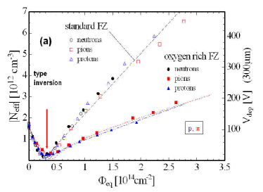
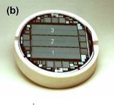
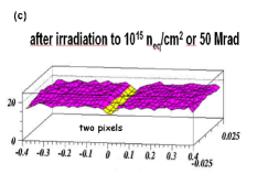
In the hybrid pixel technique sensor and FE-chips are separate parts of the detector module connected by small conducting bumps applied by using the bumping and flip-chip technology. All LHC-collider-detectors [1, 2, 3] ALICE, ATLAS, and CMS, LHCb for the RICH system [4], as well as some fixed target experiments (NA60[5] at CERN and BTeV[6] at Fermilab) employ the hybrid pixel technique to build large scale (m2) pixel detectors. Pixel area sizes are typically m m as for ATLAS or m m as for CMS. The detectors are arranged in cylindrical barrels of layers and disks covering the forward and backward regions. The main purpose of the detectors at LHC is (a) the identification of short lived particles (e.g. b-tagging for Higgs and SUSY signals), (b) pattern recognition and event reconstruction and (c) momentum measurement. The detectors need to withstand a total (10 yr) particle fluence of neq corresponding to a radiation dose of about Mrad. The discovery that oxygenated silicon is radiation hard with respect to the non-ionizing energy loss of protons and pions [7] saves pixel detectors at the LHC for which the radiation is most severe due to their proximity to the interaction point. electrode in n-bulk material sensors have been chosen to cope with the fact that type inversion occurs after about cm-2. After type inversion the -diode sits on the electrode side thus allowing the sensor to be operated partially depleted. Figure 1(a) shows the development of the effective doping concentration and the depletion voltage as a function of the fluence expected for 10 years of operation at the LHC (see also [8]). Figures 1(b) and (c) show the ATLAS pixel sensor wafer with 3 tiles [9] and the detector response after irradiation over two adjacent pixels showing a very homogeneous charge collection except for some tolerable loss at the outer edges and in an area between the pixels. These are due to the bump contact and a bias grid, respectively, which has been designed to allow testing of the sensors before bonding them to the electronics ICs.
The challenge in the design of the front-end pixel electronics [10, 11] can be summarized by the following requirements: low power ( 50W per pixel), low noise and threshold dispersion (together 200e), zero suppression in every pixel, on-chip hit buffering, and small time-walk to be able to assign the hits to their respective LHC bunch crossing. The pixel groups have reached these goals in several design iterations using first radiation-soft prototypes, then dedicated radhard designs, and finally using deep submicron technologies [11]. While CMS uses analog readout of hits up to the counting house, ATLAS obtains pulse height information by means of measuring the time over threshold (ToT) for every hit.
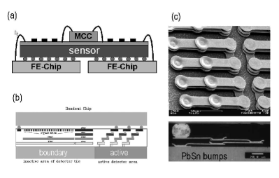
The chip and sensor connection is done by fine pitch bumping and subsequent flip-chip which is achieved with either PbSn (solder) or Indium bumps at a failure rate of . Figure 3 shows rows of m pitch bumps obtained by these techniques.
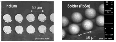
Indium bumping is done using a wet lift-off technique applied on both sides (sensor and IC) [12]. The connection is obtained by thermo-compression. The Indium joint is comparatively soft and the gap between IC and sensor is about m. PbSn bumps are applied by electroplating [13]. Here the bump is galvanically grown on the chip wafer only. The bump is connected by flip-chipping to an under-bump metallization on the sensor substrate pixel. Both technologies have been successfully used with 8” IC-wafers and 4” sensor wafers.
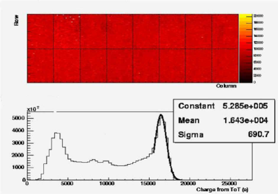
In the case of ATLAS a module of 2.1x6.4 cm2 area consists of FE-chips bump-connected to one silicon sensor. The I/O lines of the chips are connected via wire bonds to a kapton flex circuit glued atop the sensor. The flex houses a module control chip (MCC) responsible for front end time/trigger control and event building. The total thickness at normal incidence is in excess of . Figure 3 shows a 241Am (60 keV ) source scan of an ATLAS module with 46080 pixels and an amplitude spectrum obtained using the ToT analog information without clustering of pixels.
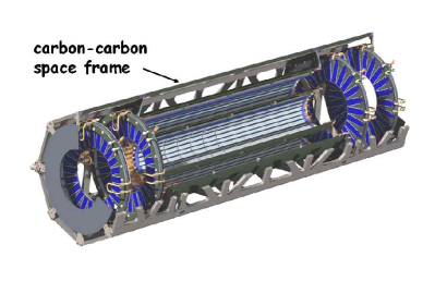
The modules are positioned by dedicated robots on carbon-carbon ladders (staves) and cooled by evaporation of a fluorinert liquid () at an input temperature below in order to maintain the entire detector below to minimize the damage induced by radiation. This operation requires pumping and the cooling tubes must stand bar pressure if pipe blocking occurs. All detector components must survive temperature cycles between and room temperature. The LHC pixel detectors are presently in production. A sketch of the final ATLAS pixel detector is shown in fig. 4.
III Trends in Hybrid Pixel Detectors
To improve the performance of Hybrid Pixel detectors in certain aspects several ideas and developments are being pursued.
III-A HAPS
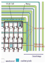
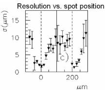
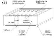
Hybrid (Active) Pixel Sensors (HAPS) [14] exploit capacitive coupling between pixels to obtain smaller pixel cells and pixel pitch with a larger readout pitch resulting in interleaved pixels. The pixel pitch is designed for best spatial resolution using charge sharing between neighbors while the readout pitch is tailored to the needs for the size of the front-end electronics cell. This way resolutions between 3m and 10m can be obtained with pixel (readout) pitches of 100m (200m) as is shown in fig. 5(b) together with the layout of a prototype sensor in fig. 5(a).
III-B MCM-D
The present hybrid-pixel modules of the LHC experiments use an additional flex-kapton fine-print layer on top of the Si-sensor (fig. 6(a)) to provide power and signal distribution to and from the module front-end chips. An interesting alternative to the flex-kapton solution is the so-called Multi-Chip-Module Technology deposited on Si-substrate (MCM-D) [16]. A multi-conductor-layer structure is built up on the silicon sensor. This allows to bury all bus structures in four layers in the inactive area of the module thus avoiding the kapton flex layer and any wire bonding at the expense of a small thickness increase of . In addition, the extra freedom in routing makes it possible to design pixel detectors which have the same pixel dimensions throughout the sensor, i.e. without larger edge pixels usually necessary to accommodate the sensor area which remains uncovered by electronics in between chips. Figure 6(b) illustrates the principle and fig. 6(c) shows scanning electron microphotographs (curtesy IZM, Berlin) of a via structure made in MCM-D technology.
III-C Active edge 3-D silicon
The features of doped Si allow interesting geometries with respect to field shapes and charge collection. So-called 3D silicon detectors have been proposed [17] to overcome several limitations of conventional planar Si-pixel detectors, in particular in high radiation environments, in applications with inhomogeneous irradiation and in applications which require a large active/inactive area ratio such as protein crystallography [18].
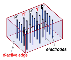
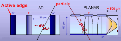
A a 3D-Si-structure (fig. 7(a)) is obtained by processing the n+ and p+ electrodes into the detector bulk rather than by conventional implantation on the surface. This is done by combining VLSI and MEMS (Micro Electro Mechanical Systems) technologies. Charge carriers drift inside the bulk parallel to the detector surface over a short drift distance of typically 50m. Another feature is the fact that the edge of the sensor can be a collection electrode itself thus extending the active area of the sensor to within about 10m to the edge. This results from the undepleted depth at this electrode. Edge electrodes also avoid inhomogeneous fields and surface leakage currents which usually occur due to chips and cracks at the sensor edges. This is seen in fig. 7(b) which shows the two structures in comparison. The main advantages of 3D-silicon detectors come from the fact that the electrode distance is short (50m) in comparison to conventional planar devices at the same total charge, resulting in a fast (1-2 ns) collection time, low ( 10V) depletion voltage and, in addition, a large active/inactive area ratio of the device.
The technical fabrication is much more involved than for planar processes and requires a bonded support wafer and reactive ion etching of the electrodes into the bulk. A compromise between 3D and planar detectors, so called planar-3D detectors maintaining the large active area, use planar technology but with edge electrodes [19], obtained by diffusing the dopant from the deeply etched edge and then filling it with poly-silicon. Prototype detectors using strip or pixel electronics have been fabricated and show encouraging results with respect to speed (3.5 ns rise time) and radiation hardness ( 1015 protons/cm2) [20].
III-D Diamond Pixel Sensors
Diamond as a potentially very radiation hard material has been explored intensively by the RD collaboration RD42 at CERN [21]. Charge collection distances up to 300m have been achieved. Diamond pixel detectors have been built with pixel electronics developed for the ATLAS pixel detector and operated as single-chip modules in testbeams [22]. A spatial resolution of = 22m has been measured with 50m pixel pitch, compared to about 12m with Si pixel detectors of the same geometry and using the same electronics. This reveals the characteristic systematic spatial shifts observed in CVD diamond due to the crystal growth. Grain structures are formed in which trapped charges at the boundaries produce polarization fields inside the sensor which cause the observed spatial shifts of the order of 100-150 m.
IV Hybrid Pixels in Imaging Applications
IV-A Counting Pixel Detectors for (Auto-)Radiography
A potentially new route in radiography techniques is the counting of individual X-ray photons in every pixel cell. This approach offers many features which are very attractive for X-ray imaging: full linearity in the response function and a principally infinite dynamic range, optimal exposure times and a good image contrast compared to conventional film-foil based radiography. It thus avoids over- and underexposed images. Counting pixel detectors must be considered as a very direct spin-off of the detector development for particle physics into biomedical applications. The analog part of the pixel electronics is in parts close to identical to the one for LHC pixel detectors while the periphery has been replaced by the counting circuitry [23].
The challenges to be addressed in order to be competitive with integrating radiography systems are: high speed ( 1 MHz) counting with a range of at least 15 bit, operation with very little dead time, low noise and particularly low threshold operation with small threshold dispersion values. In particular the last item is important in order to allow homogeneous imaging of soft X-rays. It is also mandatory for a differential energy measurement, realized so far as a double threshold with energy windowing logic [24, 25]. A differential measurement of the energy, exploiting the different shapes of X-ray spectra behind for example tissue or bone, can enhance the contrast performance of an image. Finally, for radiography high photon absorption efficiency is mandatory, which renders the not easy task of high Z sensors and their hybridization necessary.
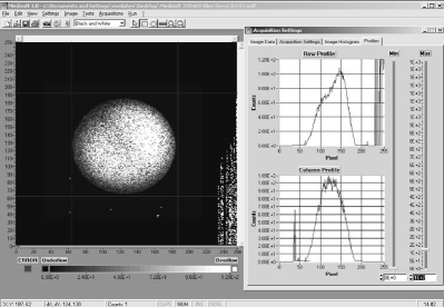
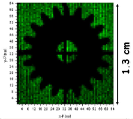
Progress with counting pixel systems have been reported at this conference [26, 27, 28]. The MEDIPIX chip developed by the MEDIPIX collaboration [29, 25] uses , 5555m2 pixels fabricated in m technology, energy windowing via two tunable discriminator thresholds, and a 13 bit counter. The maximum count rate per pixel is about 1 MHz. Figure 8 shows an image of a 55Fe point source obtained with the Medipix2 chip bonded to a 14x14 mm2, 300m thick Si sensor [26]. A similar image with a single chip CdTe detector and a higher energy 109Cd source (122 keV ) has also been taken and the capability to detect low energy beta decays from tritium has been demonstrated [26].
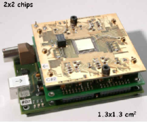
A Multi-Chip module with 2x2 chips using high-Z CdTe sensors with the MPEC chip [27] is shown in fig. 9. The MPEC chip features pixels (200200m2), double threshold operation, 18-bit counting at 1 MHz per pixel as well as low noise values (120e with CdTe sensor) and threshold dispersion (e after tuning) [30, 27]. A technical issue here is the bumping of individual die CdTe sensors which has been solved using Au-stud bumping with In-filling [31].
IV-B Protein Crystallography
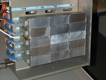
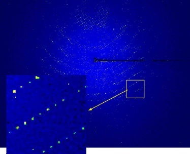
Hybrid Pixel detectors as counting imagers lead the way to new classes of experiments in protein crystallography with synchrotron radiation [34]. Here the challenge is to image, with high rate (1-1.5 MHz/pixel) and high dynamic range, many thousands of Bragg spots from X-ray photons of typically 12 keV or higher (corresponding to resolutions at the 1 range), scattered off protein crystals. The typical spot size of a diffraction maximum is m, calling for pixel sizes in the order of m. The high linearity of the hit counting method and the absence of so-called ”blooming effects”, i.e. the response of non-hit pixels in the close neighborhood of a Bragg maximum, makes counting pixel detectors very appealing for protein crystallography experiments. A systematic limitation and difficulty is the problem that homogeneous hit/count responses in all pixels, also for hits at the pixel boundaries or between pixels where charge sharing plays a role must be maintained by delicate threshold tuning. Counting pixel developments are made for ESRF (Grenoble, France) [35] and SLS (Swiss Light Source at the Paul-Scherrer Institute, Switzerland) beam lines. The PILATUS 1M detector [36] at the SLS (m m pixels) is made of fifteen 16-chip-modules each covering cm2, i.e. a total area of cm2. Figure 10(a) shows a photograph of this detector with 15 modules and close to 106 pixels covering an area of 2024 cm2 [37]. It is the first large scale hybrid pixel detector in operation. Figure 10(b) shows a Bragg image of a Lysozyme with 10s exposure to 12 keV sychrotron X-rays [37]. Many spots are contained in one pixel which is the limit of the achievable point spread resolution.
In summary hybrid pixel detectors are the present state of the art in pixel detector technology. For tracking as well as for imaging applications large (m2) detectors are being built or already in operation (PILATUS). On the negative side are the comparatively large material budget, the complicated assembling (hybridization) with potential yield pitfalls, and the difficulty to obtain high assembly yields with non-wafer scale high-Z sensor materials. As trends within this technology, interleaved pixels and MCM-D promise better resolution and more homogeneous modules, while 3D-silicon detectors can address applications in high radiation environments or those where a large active/inactive area ratio is mandatory.
V Monolithic and Semi-Monolithic Pixel Detectors
Monolithic pixel detectors, in which amplifying and logic circuitry as well as the radiation detecting sensor are one entity, produced in a commercially available technology, are the dream of semiconductor detector developers. This will not be possible in the near future without compromising. Developments and trends in this direction have much been influenced by RD for vertex tracking detectors at future colliders such as a Linear Collider [38]. Very low (1 X0) material per detector layer, small pixel sizes (20mm) and a good rate capability (80 hits/mm2/ms) is required, due to the very intense beamstrahlung of narrowly focussed electron beams close to the interaction region which produce electron positron pairs in vast numbers. High readout speeds of MHz line rate with 40s frame time are necessary.
Among the developments of monolithic or semi-monolithic pixel devices perhaps the following classifying list can be made.
-
-
Non-standard CMOS on high resistivity bulk
The first monolithic pixel detector, successfully operated in a particle beam already in 1992 [39], used a high resistivity p-type bulk p-i-n detector in which the junction had been created by an n-type diffusion layer. On one side, an array of ohmic contacts to the substrate served as collection electrodes (fig. 11(a)). Due to this only simple pMOS transistor circuits sitting in n-wells were possible in the active area. The technology was certainly non-standard and non-commercial. No further development emerged. -
-
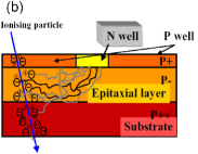
CMOS technology with charge collection in epi-layer
Commercial CMOS technologies use low resistivity silicon which is not suited for charge collection. However, in some technologies an epitaxial silicon layer of a few to 15m thickness can be used [40, 41, 42]. The generated charge is kept in the epi-layer by potential wells at the boundary and reaches an n-well collection diode by thermal diffusion (fig. 11(b)). The signal charge is therefore very small (1000e) and low noise electronics is a real challenge. As this development uses standard processing technologies it is potentially very cheap. Despite using CMOS technology the potential of full CMOS circuitry in the active area is not available (only nMOS) because of the n-well/p-epi collecting diode which does not permit other n-wells.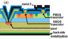
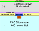
Figure 12: (a) Cross section through a monolithic CMOS on SOI pixel detector using high resistivity silicon bulk insolated from the low resistivity CMOS layer with connecting vias in between [15, 47], (b) cross section through a structure using amorphous silicon on top of standard CMOS VLSI electronics [48, 49]. -
-
CMOS on SOI (non-standard)
In order to exploit high resistivity bulk material, the authors of [47] develop pixel sensors with full CMOS circuitry using the Silicon-on-Insulator (SOI) technology. The connection to the charge collecting bulk is done by vias (fig. 12(a)). The technology offers full charge collection in 200–300m high resistive silicon with full CMOS electronics on top. At present the technology is however definitely not a commercial standard and the development is still in its beginnings. -
-
Amorphous silicon on standard CMOS ASICs
Hydrogenated amorphous-Silicon (a-Si:H), where the H-content is up to 20, can be put as a film on top of CMOS ASIC electronics. a-Si:H has been studied as a sensor material long ago and has gained interest again [48, 49] with the advancement in low noise, low power electronics. The signal charge collected in the 30m thick film is in the range of 500-1500 electrons. A cross section through a typical a-Si:H device is shown in fig. 12(b). From a puristic view it is more a hybrid technology, but the main disadvantage of the hybridization connection is absent. The radiation hardness of these detectors appears to be very high 1015cm-2 due to the defect tolerance and defect reversing ability of the amorphous structure and the larger band gap (1.8 eV). The carrier mobility is very low ( = 2-5 cm2/Vs, = 0.005 cm2/Vs), i.e. essentially only electrons contribute to the signal. Basically any CMOS circuit and IC technology can be used and technology changes are uncritical for this development. For high-Z applications poly-crystalline HgI2 constitutes a possible semiconductor film material. The potential advantages are small thickness, radiation hardness, and low cost. The development is still in its beginnings and – as for CMOS active pixel sensors – a real challenge to analog VLSI design. -
-
Amplification transistor implanted in high resistivity bulk
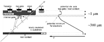
In so-called DEPFET pixel sensors [50] a JFET or MOSFET transistor is implanted in every pixel on a sidewards depleted [56] bulk. Electrons generated by radiation in the bulk are collected in a potential minimum underneath the transistor channel thus modulating its current (fig. 13). The bulk is fully depleted rendering large signals. The small capacitance of the internal gate offers low noise operation. Both together can be used to fabricate thin devices. The sensor technology is non-standard and the operation of DEPFET pixel detectors requires separate steering and amplification ICs (see below).
Because CMOS active pixels and DEPFET pixels are most advanced in their development, they are discussed in more detail below.
V-A CMOS Active Pixels
The main difference of CMOS monolithic active pixel sensors [40] to CMOS camera chips is that they are larger in area and must have a 100 fill factor for efficient particle detection. Standard commercial CMOS technologies are used which have a lightly doped epitaxial layer between the low resistivity silicon bulk and the planar processing layer. The epi-layer is – technology dependent – at most 15m thick and can also be completely absent. Collaborating groups around IReSLEPSI [42, 43], RAL [44] and Irvine-LBNL-Ohio [45] use similar approaches to develop large scale CMOS active pixels also called MAPS (Monolithic Active Pixel Sensors) [41]. Prototype detectors have been produced in m, m and m CMOS technologies [54, 52].
In the MAPS device (fig. 11(b)) electron-hole pairs created by ionization energy loss in the epitaxial layer remain trapped between potential barriers on both sides of the epi-layer and reach, by thermal diffusion, an n-well/p-epi collection diode. The sensor is depleted only directly under the n-well collection diode where full charge collection is obtained; the charge collection is incomplete in all other areas. With small pixel cells collection times in the order of are obtained. The signal is small, some hundred to 1000e, depending on the thickness of the epi-layer. A chip submission using a process with no epi-layer, but with a low doped substrate of larger resistivity has also been tried (MIMOSA-4) [53] which proved to function with high detection efficiency for minimum ionizing particles. This renders the uncertainty and dependence on the future of the epi-layer thickness in different technologies less constraining.
Matrix readout performed using a standard 3-transistor circuit (line select, source-follower stage, reset) commonly employed by CMOS matrix devices, but can also include current amplification and current memory [54]. For an image two complete frames are subtracted from each other (CDS) which suppresses switching noise. Noise figures of 10-30e and S/N 20 have been achieved with spatial resolutions below 5m. The radiation hardness of CMOS devices is always a crucial question for particle detection in high intensity colliders. MAPS appear to sustain non-ionizing radiation (NIEL) to 1012neq while the effects of ionizing radiation damage (IEL) are at present still unclear [55]. Apart from this the focus of further development lies in making larger area devices and in increasing the charge collection performance in the epi-layer. For the former, first results in reticle stitching, that is electrically connecting IC area over the reticle border, have been encouraging (fig. 14(a)) [52]. Full CMOS stitching over the reticle boarder still has to be demonstrated. The poor charge collection by thermal diffusion is another area calling for ideas. Approaches using more than one n-well collecting diode [44], a photo-FET [54, 42, 43], or a photo-GATE [46] are currently investigated. The photo-FET called technique (fig. 14(b)) has features similar to those of DEPFET pixels (see below). A pMOS FET is implanted in the charge collecting n-well and signal charges affect its gate voltage and modulate the transistor current.
Above all, the advantages of a fully CMOS monolithic device relate to the adoption of standard VLSI technology and its resulting low cost potential (potentially 25 per cm2). In turn the disadvantages also come largely from the dependence on commercial standards. The thickness of the epi-layer varies for different technologies. It becomes thinner for smaller processes and with it also the number of produced signal electrons vanishes. Only a few processing technologies are suited. With the rapid change of commercial process technologies this is an issue of concern. The fact that good detector performance has been seen with non-epi wafers material provides some relief. Furthermore, in the active area, due to the n-well collection diode, no CMOS (only nMOS) circuitry is possible. The voltage signals are very small (mV), of the same order as transistor threshold dispersions requiring very low noise VLSI design. The radiation tolerance of CMOS pixel detectors for particle detection beyond 1012 neq is still a problem although the achieved tolerance should be sufficient for a Linear Collider. Improved readout concepts and device development for high rate particle detection at a linear collider is under development [38]. For the upgrade of the STAR microvertex detector the use of CMOS active pixels is planned [54].
V-B DEPFET Pixels
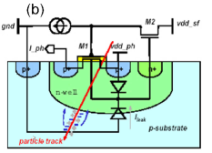
The Depleted Field Effect Transistor structure (DEPFET) [50] provides detection and amplification properties jointly and has been experimentally confirmed and successfully operated as single pixel structures and as large (64x64) pixel matrices [51]. The DEPFET detector and implanted amplification structure is shown in fig. 13. Sidewards depletion [56] provides a parabolic potential which has – by appropriate biasing and a so-called deep-n implantation – a local minimum for electrons (m) underneath the transistor channel. The channel current can be steered and modulated by the voltage at the external gate and - important for the detector operation - also by the deep-n potential (internal gate). Electrons collected in the internal gate are removed by a clear pulse applied to a dedicated CLEAR contact outside the transistor region or by other clear mechanisms. The very low input capacitance ( few fF) and the in situ amplification makes DEPFET pixel detectors very attractive for low noise operation [57]. Amplification values of 400 pA per electron collected in the internal gate have been achieved. Further amplification enters at the second level stage (current based readout chip).
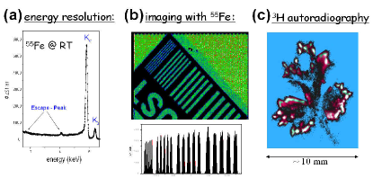
DEPFET pixels are currently being developed for three very different application areas: vertex detection in particle physics [58, 59], X-ray astronomy [60] and for biomedical autoradiography [57]. Figure 15 summarizes the achieved performance in noise and energy resolution with single pixels structures (fig. 15(a)) and in spatial resolutions with 64x64 pixels matrices (fig. 15(b)). With round single pixel structures noise figures of 2.2e at room temperature and energy resolutions of 131 keV for 6 keV X-rays have been obtained. With small (20x30 m2) linear structures fabricated for particle detection at a Linear Collider the noise figures are about 10e. The spacial resolution read off from fig. 15(b) in matrices operated with 50 kHz line rates is [59]
The capability to observe tritium in autoradiographical applications is shown in fig. 15(c).
The very good noise capabilities of DEPFET pixels are very important for low energy X-ray astronomy and for autoradiography applications. For particle physics, where the signal charge is large in comparison, this feature is used to design very thin detectors (50m) with very low power consumption when operated as a row-wise selected matrix [59]. Thinning of sensors to a thickness of 50m using a technology based on deep anisotropic etching has been successfully demonstrated [61]. For the development of DEPFET pixels for a Linear Collider matrix row rates of 50 MHz and frame rates for 520x4000 pixels of 25 kHz, read out at two sides, are targeted. Sensors with cell sizes of 20x30m2 have been fabricated and complete clearing of the internal gate, which is important for high speed on-chip pedestal subtraction, has been demonstrated [59]. A large matrix is readout using sequencer chips for row selection and current based chip for column readout [59]. Both chips have been developed at close to the desired speed for a Linear Collider. The estimated power consumption for a five layer DEPFET pixel vertex vertex detector is only 5W rendering a very low mass detector without cooling pipes feasible. The most recent structures use MOSFETs as DEPFET transistors for which the radiation tolerance still has to be investigated.
VI Summary
Driven by the demands for high spatial resolution and high rate particle detection in high energy physics, semiconductor pixel detectors have started to also become exploited for imaging applications. Hybrid pixel detectors, in which sensor and electronic chip are separate entities, connected via bump bonding techniques represent today’s state of the art for both, particle detection and imaging applications. New trends include interleaved pixels having different pixel- and readout-pitches, MCM-D structures and 3D-silicon detectors with active edges. Monolithic or semi-monolithic detectors, in which detector and readout ultimately are one entity, are currently developed in various forms, largely driven by the needs for particle detection at future colliders. CMOS active pixel sensors using standard commercial technologies on low resistivity bulk and SOI pixels, a-SI:H, and DEPFET-pixels, which try to maintain high bulk resistivity for charge collection, classify the different ways to monolithic detectors which are presently carried out.
Acknowledgment
The author would like to thank W. Dulinski, M. Caccia, P. Jarron, P. Russo, C. da Via’, and S. Parker for providing new material and information for this presentation.
References
-
[1]
Technical Design Report of the ATLAS Pixel Detector,
CERN/LHCC/98-13 (1998);
N. Wermes, Design and Prototype Performance of the ATLAS Pixel Detector, Nucl. Inst. Meth. A447 (2002) 121-128. -
[2]
CMS, the Tracker System Project, Technical Design Report,
CERN/LHCC/98-006 (1998);
W. Erdmann, The CMS pixel detector, Nucl. Inst. Meth. A447 (2000) 178-83. -
[3]
ALICE Technical Design Report, CERN/LHCC 99-12 (1999);
P. Chochula et al., The ALICE Silicon Pixel Detector, Nucl. Phys. A 715 (2003) 849-852. - [4] T. Gys, The pixel hybrid photon detectors for the LHCb-RICH project, Nucl. Inst. Meth. A465 (2001) 240-246.
-
[5]
A. Baldit et al., CERN-SPSC-2000-010 (2000);
C. Lourenco, E. Radermacher, CERN-SPSC-2002-025 (2002). - [6] S. Kwan (BTeV Collaboration), The BTEV Pixel and Microstrip Detectors, Nucl. Inst. Meth. A511 (2003) 48-51.
-
[7]
ROSE Collaboration, G. Lindström et al.,
Nucl. Inst. Meth. A466 (2001) 308-326;
G. Lindström, Radiation Damage in Silicon Detectors, Nucl. Inst. Meth. A512 (2003) 92. - [8] O. Krasel et al., Measurement of the trapping time constants in Proton-Irradiated Silicon Pad Detectors, IEEE Nuclear Science Symposium Portland 2003, these proceedings.
- [9] M. S. Alam et al., The ATLAS Silicon Pixel Sensors, Nucl. Inst. Meth. A456 (2001) 217-232.
- [10] L. Blanquart et al. Analog front-end cell designed in a commercial 0.25 m process for the ATLAS pixel detector at LHC, IEEE Trans. Nucl. Sci. vol.49(4), (2002) 1778-1782
- [11] L. Blanquart et al., FE-I2: A Front-End Readout Chip Designed in a commercial 0.25 m Process for the ATLAS Pixel detector at LHC, IEEE Nuclear Science Symposium Portland 2003, these proceedings.
- [12] C. Gemme, Study of Indium bumping for the ATLAS pixel detector, Nucl. Inst. Meth. A465 (2001) 200–203.
-
[13]
G. Engelmann, J. Wolf, L. Dietrich, S. Fehlberg, O. Ehrmann and
H. Reichl, Proc. 1999 Joint International Meeting of the
Electrochemical Society, Hawaii 1999, Vol. 99-2 p. 907;
J. Wolf, PbSn60 Solder Bumping by Electroplating, Pixel2000 Workshop, Genova, Italy, June 2000. - [14] W. Kucewicz, G. Deptuch, A. Zalewska, M. Battaglia, K. Osterberg, R. Orava, M. Caccia, C. Meroni, G. Vegni, P. Grabiec, B. Jaroszewicz, J. Marczewski, Capacitively coupled active pixel sensors with analog readout for future e+e- colliders, Acta Phys.Polon. B30 (1999) 2075–2083.
- [15] M. Amati, M. Baranski, A. Bulgheroni, M. Caccia, K. Domanski, P. Grabiec, M. Grodner, B. Jaroszewicz, W. Kucewicz, K. Kucharski, S. Kuta, W. Machowski, J. Marczewski, H. Niemiec, M. Sapor, D. Tomaszewski, Hybrid Active Pixel Sensors and SOI Inspired Option, Nucl. Inst. Meth. A511 (2003) 265–270.
-
[16]
P. Gerlach, C. Linder, K.H. Becks, Nucl. Inst. Meth. A473 (2001) 102-106 and
references therein;
M. Töpper, Intl. Conf. on High Density Packaging and MCMs, Denver, Colorado, April 1999. -
[17]
C. Kenney, S. Parker, J. Segal, C. Storment, Silicon
detectors with 3-D electrode arrays: fabrication and initial test
results, IEEE Trans. Nucl. Sci. vol.46(4), (1999) 1224–1236;
C.J. Kenney, S.I. Parker, B. Krieger, B. Ludewigt, T.P. Dubbs, H. Sadrozinski, Observation of beta and X rays with 3-D-architecture silicon microstrip sensors, IEEE Trans. Nucl. Sci. vol.48(2), (2001) 189-193;
C.J. Kenney, S. Parker, E. Walckiers, Results from 3-D silicon sensors with wall electrodes: near-cell-edge sensitivity measurements as a preview of active-edge sensors, IEEE Trans. Nucl. Sci. vol.48(6), (2001) 2405. -
[18]
E. M. Westbrook, Pixels and Proteins: Better Detectors for
Biological Crystallography, Review given at IEEE Nuclear Science Symposium, Portland Oct. 2003, these proceedings;
S.I. Parker, C.J. Kenney, J.D. Segal, E. Westbrook, J. Hasi, C. Da Via’, E. Mandelli, G. Meddeleer, J. Morse, Direct X-ray Detector with 3D Silicon Pixel Sensors for Structural Molecular Biology, IEEE Nuclear Science Symposium Portland 2003, these proceedings. - [19] C.J. Kenney, E. Westbrook, J.D. Segal, S.I. Parker, J. Morse, J. Hasi, C. Da Via’, First Results from Active-Edge, Planar radiation Sensors, IEEE Nuclear Science Symposium Portland 2003, these proceedings.
-
[20]
S.I. Parker, A. Kok, C. Da Via’, J. Hasi, G. Anelli, P. Jarron,
C.J. Kenney, J.D. Segal, Measurements of Fast Rise-time
Pulses from 3D Silicon Sensors, IEEE Nuclear Science Symposium Portland 2003, these proceedings;
C.J. Kenney, E. Westbrook, J.D. Segal, E. Perozzielo, S.I. Parker, J. Hasi, C. Da Via’, J. Morse, First Results from Active Edge 3D Architecture radiation Sensors, IEEE Nuclear Science Symposium Portland 2003, these proceedings. -
[21]
RD42 Collaboration, Diamond as a particle detector, Proc.
Itatial Phys. Socienty, Torino, vol. 52 (1996), 105;
R. Wedenig et al., CVD Diamond Pixel Detectors for LHC Experiments, Nucl. Phys. B. (Proc. Suppl.) 78 (1999) 497. - [22] M. Keil et al., New Results on Diamond Pixel Sensors using ATLAS Frontend Electronics, Nucl. Inst. Meth. A501 (2003) 153-159.
- [23] P. Fischer, An area efficient 128 channel counter chip, Nucl. Inst. Meth. A378 (1996) 297–300.
-
[24]
P. Fischer, A. Helmich, M. Lindner, N. Wermes, L. Blanquart,
A Photon Counting Chip with Energy Windowing,
IEEE Trans. Nucl. Sci. vol.47(3), (2000) 881–884;
M. Lindner, L. Blanquart, P. Fischer, H. Krüger, N. Wermes, Medical X-ray imaging with energy windowing, Nucl. Inst. Meth. A465 (2000) 229–234. - [25] X. Llopart, M. Campbell, R. Dinapoli, D. SanSegundo, E. Pernigotti, Medipix2: A 64-k pixel readout chip with 55- mu m square elements working in single photon counting mode, IEEE Trans. Nucl. Sci. vol.49(5), (2002) 2279–2283.
-
[26]
G. Mettivier, M.C. Montesi, P. Russo, Digital
Autoradiography with a Medipix2 Hybrid Silicon Pixel Detector,
Poster given at IEEE Medical Imaging Conference, Portland Oct. 2003;
G. Mettivier, M.C. Montesi, P. Russo, Tritium digital autoradiography with a Medipix2 hybrid silicon pixel detector, submitted to Nucl. Inst. Meth. A - [27] M. Löcker, P. Fischer, M. Kouda, S. Krimmel, H. Krüger, M. Lindner, K. Nakazawa, T. Takahashi, N. Wermes, Single photon Counting X-ray Imaging with Si and CdTe Single Chip Pixel Detectors and Multichip Pixel Modules, IEEE Nuclear Science Symposium Portland 2003, these proceedings.
- [28] F. Edling, R. Brenner, N. Bingefors, K. Fransson, L. Gustafsson, L. del Risco Norrlid, C. Rönnqvist, A Hybrid Pixel Detector with Two Counters for X-ray Imaging, Poster given at IEEE-NS Symposium, Portland Oct. 2003, these proceedings.
- [29] Medipix Collaboration, S.R. Amendiola et al., Nucl. Inst. Meth. A466 (2001) 74-78.
-
[30]
P. Fischer, J. Hausmann, A. Helmich, M. Lindner, N. Wermes, L.
Blanquart, A counting pixel readout chip and sensor system
for X-ray imaging, IEEE Trans. Nucl. Sci., Vol 46, No. 4
(1999)1070 ;
L. Blanquart, V. Bonzon, G. Comes, P. Delpierre, P. Fischer, J. Hausmann, M. Keil, M. Lindner, S. Meuser, N. Wermes, Pixel Readout Electronics for LHC and Biomedical Applications, Nucl. Inst. Meth. A439 (2000) 80–90. - [31] P. Fischer, M. Kouda, H. Krüger, M. Lindner, G. Sato, T. Takahashi, S. Watanabe, N. Wermes, A counting CdTe pixel detector for hard X-ray and gamma-ray imaging, IEEE Trans. Nucl. Sci. vol.48, (2001) 2401-2404.
-
[32]
T. Ducourant, M. Michel, G. Vieux, T. Peppler, J.C. Trochet, R.F.
Bastiaens, F. Busse, Optimization of key building blocks
for a large-area radiographic and fluoroscopic dynamic digital
X-ray detector based on a-Si:H/CsI:Tl flat panel technology,
Proc. SPIE 3977 (2000) 14-25;
N. Jung et al., Proc. SPIE 3336 (1998) 396-407. - [33] O. Tousignant, M. Choquette, Y. Demers, L. Laperriere, J. Leboeuf, M. Honda, M. Nishiki, A. Takahashi, A. Tsukamoto, Progress report on the performance of real-time selenium flat-panel detectors for direct X-ray imaging, Proc. SPIE 4682 (2002) 503-510.
- [34] H. Graafsma, Detector Needs at Current and Future Synchrotron Sources, Review given at IEEE Nuclear Science Symposium, Portland Oct. 2003, these proceedings.
-
[35]
P. Delpierre, J.F. Berar, L. Blanquart, B. Caillot, J.C. Clemens,
C. Mouget, IEEE Trans. Nucl. Sci. vol.48(4), (2001) 987-991;
P. Delpierre, J.F. Berar, L. Blanquart, N. Boudet, P. Breugnon, B. Caillot, J.C. Clemens, I. Koudobine, C. Mouget, R. Potheau, I. Valin, NSS-MIC/IEEE, San Diego (USA), Nov 4-10, 2001, accepted for publication in IEEE Trans. Nucl. Sci., Sept. 2002. - [36] C. Brönnimann et al., Journal of Syn. Rad. 7 (2000) 301.
- [37] E. Eikenberry, C. Broennimann, G. Huelsen, H. Toyokawa, M. Suzuki, R. Horisberger, B. Schmitt, C. Schulze-Briese, T. Tomizaki, The PILATUS X-ray Detector, 13th International Workshop on Room-Temperature Semiconductor X- and Gamma-Ray Detectors, Portland 2003.
- [38] TESLA Technical Design Report, Vol. IV, DESY-01-011 (2001).
- [39] W. Snoeys, J. Plummer, S. Parker, C. Kenney, A new integrated pixel detector for high energy physics, IEEE Trans. Nucl. Sci. vol.39, (1992) 1263–1269.
-
[40]
B. Dierickx, G. Meynants, D. Scheffer, Near 100 fill
factor CMOS active pixel, Proc. IEEE CDDAIS Workshop, Brugge,
Belgium, June 1997 ;
G. Meynants, B. Dierickx, D. Scheffer, CMOS active pixel image sensor with CCD performance, Proceedings SPIE - Int. Soc. Opt. Eng. (USA), vol.3410 (1998) 68–76, 9. - [41] R. Turchetta, J.D. Bertst, B. Casadei, G. Claus, C. Colledani, W. Dulinski, Y. Hu, D. Husson, J.-P. Le-Normand, J.L. Riester, G. Deptuch, U. Goerlach, S. Higueret, M. Winter, A monolithic active pixel sensor for charged particle tracking and imaging using standard VLSI CMOS technology, Nucl. Inst. Meth. A458 (2001) 677-689; G. Claus, C. Colledani, W. Dulinski, D. Husson, R. Turchetta, J.L. Riester, D. Deptuch, G. Orazi, M. Winter, Particle tracking using CMOS monolithic active pixel sensor, Nucl. Inst. Meth. A465 (2001) 120–124.
-
[42]
G. Deptuch, W. Dulinski, Y. Gornushkin, C. Hu-Guo, I. Valin,
Monolithic Active Pixel Sensor with on-pixel amplification
and Double Sampling Operation, Nucl. Inst. Meth. A512 (2003) 299-309;
G. Claus et al., Monolithic Active Pixel Sensors for a Linear Collider, Nucl. Inst. Meth. A473 (2001) 83–85. - [43] G. Deptuch et al., Monolithic Active Pixel Sensor with In-pixel Double Sampling and Columns-level Disrcrimination, Poster submitted to this conference.
- [44] R. Turchetta et al., Monolithic Active Pixel Sensors (MAPS) for Particle Physics and Space Science, Proceedings VERTEX 2003, Lake Windermere, UK, September 2003.
- [45] H. Matis, F. Bieser, S. Kleinfelder, G. Rai, F. Retiere, H. Ritter, K. Singh, S. Wurzel, H. Wiemann, E. Yamamoto, Charged Particle Detection using a CMOS Active Pixel Sensor, IEEE Trans. Nucl. Sci. vol.50, (() 2003)1020-1025.
- [46] S. Kleinfelder, F. Bieser, Y. Chen, I. Kotov, H.S. MAtis, M. Oldenburg, F. Retiere, K.D. Singh, H.H. Wiemann, E. Yamamoto, Novel Integrated CMOS Pixel Structures for Vertex Detectors, IEEE Nuclear Science Symposium Portland 2003, these proceedings.
- [47] J. Marczewski, K. Domanski, P. Grabiec, M. Grodner, B. Jaroscewicz, A. Kociubinski, D. Tomaszewski, W. Kucewicz, S. Kuta, W. Machowski, H. Niemiec, M Sapor, M. Caccia, SOI Active Pixel Detectors of Ionizing Radiation - Technology and Design Development, IEEE Nuclear Science Symposium Portland 2003, these proceedings.
- [48] J.A. Theil et al., a-Si:H photodiode technology for advanced CMOS active pixel sensor imagers, 19th Intl. Conf. on Amorphous Materials and Semiconductors, Nice, France, August 2001
- [49] P. Jarron, Deposition of amorphous silicon above integrated circuits, 19th Intl. Conf. on Advanced Detectors, Elba, Italy, May 2003
- [50] J. Kemmer, G. Lutz, New Semiconductor Detector Concepts, Nucl. Inst. Meth. A253 (1987) 356.
-
[51]
W. Neeser et al., The DEPFET Pixel BIOSCOPE,
IEEE Trans. Nucl. Sci. vol.47(3), (2000) 1246;
P. Klein et al., A DEPFET Pixel Bioscope for the Use in Autoradiography, Nucl. Inst. Meth. A454 (2000) 152–157;
J. Ulrici, S. Adler, P. Buchholz, P. Fischer, P. Klein, M. Löcker, G. Lutz, W. Neeser, L. Strüder, M. Trimpl, N. Wermes, Spectroscopic and imaging performance of DEPFET pixel sensors, Nucl. Inst. Meth. A465 (2001) 247–252. - [52] A. Gay et al., High Resolution CMOS Sensors for a Vertex Detector at the Linear Collider, Vertex03 Conference, Lake Windermere, UK, September 2003, Proceedings.
- [53] W. Dulinski et al., CMOS Monolithic Active Pixel Sensors for Minimum Ionizing Particle Tracking using non-epitaxial silicon substrate, IEEE Nuclear Science Symposium Portland 2003, these proceedings.
- [54] W. Dulisnki et al., CMOS monolithic active pixel sensors for high resolution particle tracking and ionizing radiation imaging, Frontier Detectors for Frontier Physics 2003, Elba, May 2003.
- [55] W. Dulinksi, private communication.
- [56] E. Gatti, P. Rehak, Semiconductor driftchamber-An application of a novel charge transport scheme, Nucl. Inst. Meth. A225 (1984) 608.
-
[57]
J. Ulrici, S. Adler, P. Buchholz, P. Fischer, P. Klein, M. L cker,
G. Lutz, W. Neeser, L. Str der, M. Trimpl, N. Wermes,
Spectroscopic and imaging performance of DEPFET pixel
sensors, Nucl. Inst. Meth. A465 (2001) 247 ;
J. Ulrici, P. Fischer, P. Klein, G. Lutz, W. Neeser, R. Richter, L. Str der, M. Trimpl, N. Wermes, Imaging Performance of a DEPFET Bioscope system in Tritium Autoradiography, submitted to IEEE Trans. Nucl. Sci. vol., (2003) . -
[58]
P. Fischer, et al., Desy Linear Collider Note
LC-DET-2002-004 (2002) and Desy PRC RD 03/01;
M. Trimpl, L. Andricek, P. Fischer, G. Lutz, R.H. Richter, L. Struder, J. Ulrici, N. Wermes, A fast readout using switched current techniques for a DEPFET-pixel vertex detector at TESLA, Nucl. Inst. Meth. A511 (2003) 257–264;
R.H. Richter, L. Andricek, P. Fischer, K. Heinzinger, P. Lechner, G. Lutz, I. Peric, M. Reiche, G. Schaller, M. Schnecke, F. Schopper, H. Soltau, L. Struder, J. Treis, M. Trimpl, J. Ulrici, N. Wermes, Design and Technology of DEPFET Pixel Sensors for Linear Collider Applications, Nucl. Inst. Meth. A511 (2003) 250–256. - [59] N. Wermes, New Results on DEPFET Pixel Detectors for Radiation Imaging and High Energy Particle Detection, IEEE Nuclear Science Symposium Portland 2003, these proceedings.
-
[60]
P. Holl, P. Fischer, P. Klein, G. Lutz, W. Neeser, L. Strüder,
N. Wermes, Active Pixel Matrix for X-ray Satellite
Missions, IEEE Trans. Nucl. Sci. vol.47(4), (2000) 1441–1425;
L. Strüder et al., Proc. SPIE Vol. 4012 (2000) 200–217;
L. Strüder, 13th International Workshop on Room-Temperature Semiconductor X- and Gamma-Ray Detectors, Portland 2003. - [61] L. Andricek, Processing of Ultra Thin Silicon Sensors for Future Linear Collider Experiments, IEEE Nuclear Science Symposium Portland 2003, these proceedings.