Current address: ] van der Waals-Zeeman Instituut, Universiteit van Amsterdam, Valckenierstraat 65, 1018 XE Amsterdam, The Netherlands Current address: ] Centre for Atom Optics and Ultrafast Spectroscopy, Swinburne University of Technology, Hawthorn 3122, Australia
Calibration of a single atom detector for atomic micro chips
Abstract
We experimentally investigate a scheme for detecting single atoms magnetically trapped on an atom chip. The detector is based on the photoionization of atoms and the subsequent detection of the generated ions. We describe the characterization of the ion detector with emphasis on its calibration via the correlation of ions with simultaneously generated electrons. A detection efficiency of 47.8 2.6% is measured, which is useful for single atom detection, and close to the limit allowing atom counting with sub-Poissonian uncertainty.
pacs:
32.80.Pj 32.80.Rm 41.75.Ak 42.50.-p 42.79.AgI Introduction
Trapping and manipulating a small number of cold atoms in optical or magnetic traps is one of the most intriguing fields of research with ultra cold atoms. Degenerate quantum gases with small atom numbers allow for the investigation of physics beyond the mean field approach such as the Mott-Insulator transition Greiner2002a , revival of coherence Greiner2002b , number squeezing chuu2005 ; Jo2006a ; li2007 , Tonks-Girardau gases Paredes2004a ; Kinoshita2004a and Luttinger liquids Voit1995a ; Wonneberger2006a . Furthermore controlled quantum engineering of few atom entanglement is a mandatory prerequisite for quantum computation with cold atoms. The implementation of such scenarios is one of the main motivations for trapping atoms in miniaturized magnetic traps near the surface of a microchip Zimmermann2007a . In addition, such magnetic micro traps offer unique opportunities for atom interferometry Jo2006a ; Schumm2005a ; wang2005 ; Guenther2006a and surface diagnostics Wildermuth2005a ; Guenther2005a .
To date, micro traps are exclusively operated with ensembles such as clouds of thermal atoms or quantum degenerate gases Zimmermann2007a . The ability to detect single atoms near the surface of a chip would open the door to a new class of experiments. Besides future applications in quantum computation birkl2007 , a continuous flux of atoms transmitted through an on-chip atom interferometer could for instance be detected in real time while the resonance of the interferometer is varied. A complete interferometer spectrum could thus be recorded with atoms from a single Bose-Einstein condensate. In combination with an integrated atom laser fortagh2003a , a sensitive matter wave based spectrometer could be realized similar to its optical analog involving tunable lasers and photo detectors.
Besides the well known experiments with single atoms in cavities Pinkse2000a ; Haroche2001a , there has recently been significant progress towards the detection of single cold atoms. In the special situation of metastable helium, direct single atom detection with micro channel plates is possible due to the large internal energy of the atoms that is released at the surface of the detector Schellekens2005a ; Jeltes2006a . Sensitive single atom detection has also been demonstrated with optical cavities placed either at some distance from the atom source Bourdel2006a or, very recently, integrated on an atom chip Teper2006a ; Treutlein2006a . Alternatively, the atoms can be ionized by optical excitation with the resulting ions being subsequently detected with a suitable ion detector. Photoionization of atoms in an atom chip trap has recently been demonstrated Kraft2007a . By introducing an efficient ion detector that is compatible with the chip geometry, single atom detection is possible.
In this paper we experimentally investigate an ion detection scheme that is compatible with atom chip traps. The first step of single atom detection i.e. the photoionization of atoms in the micro trap, is described elsewhere Kraft2007a . Here, we describe the ion detection scheme and demonstrate a calibration procedure for a single ion detector which involves ionizing a large number of atoms and correlating the ions with the simultaneously generated electrons. The experimentally observed ion detection efficiency of about 50% is limited mainly by the sensitivity of the channel electron multiplier (CEM) used for ion detection. There are standard methods to increase this sensitivity. The total sensitivity would then exceed the critical single atom detection efficiency of 50% which marks the threshold above which total atom number determination with sub-Poissonian resolution is in principle possible campey2006a .
II Ion detection scheme
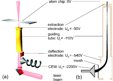
The proposed ion detection scheme is shown in Fig. 1(a). Single atoms propagating in a magnetic waveguide near the surface of an atom chip are photoionized by stepwise excitation with two co-axial laser beams Kraft2007a . The beams are oriented perpendicular to the chip surface and pass through it via a 150 m diameter hole. This allows the detection of atoms at very small distances from the surface of 1 m and below. Ionization occurs within the 30 m beam waist and the spatial selectivity of ionization could potentially be reduced further to 100 nm Kraft2007a . To allow optical access to the trapped atoms and to create a well-defined detection region, ion optics are used to guide the ions away from the chip and into the CEM. To allow access for the ionization lasers, the CEM is mounted at the end of the ion optics at 90∘ to the axis of the laser beams, and an additional electrode deflects the ions into the CEM.
The first part of the ion optics consists of a disc (extraction electrode) of 8 mm diameter which is placed parallel to the chip surface at a distance of 1.6 mm. The chip is grounded and the extraction electrode is biased at a negative voltage , creating an electric field in the region between them. This field accelerates the ions from the ionization region towards a 1 mm diameter aperture in the the extraction electrode, through which they enter a 36 mm long tube set to a voltage . The two electrodes together form a lens which focuses the ions within the tube. At the end of the tube, 40 mm from the extraction electrode, a third electrode, set to voltage , deflects the ions, which leave the ion optics through a fine mesh with 87% transmission. Outside the ion optics they are attracted by the horn of the CEM burle set to a negative voltage . Any ions produced by the ionisation lasers within the ion optics are screened from the CEM potential by the mesh. At the surface of the CEM an ion impact causes the emission of secondary electrons which starts an avalanche inside the multiplier tube. The resulting charge pulse is observed with standard counting electronics srs .
Fig. 1(b) shows numerically simulated ion trajectories for this setup. To a very good approximation, the ions move along straight lines normal to the surface of the extraction electrode such that the ion detection volume is simply given by the projection of the extraction electrode aperture. This means that ions can only be detected from the cylindrical region of diameter 1 mm running between the aperture and the chip, effectively eliminating background counts.
III Detector calibration
In order to calibrate the ion detector we made use of a scheme in which atoms are ionized and the resulting electrons and electron-ion coincidences are detected and counted campey2006a ; ncrp . By only counting ions for which the correlated electron is also detected, it is possible to measure the ion detection efficiency without any knowledge of the electron detection efficiency. If atoms are ionized, the number of electrons detected, corrected for background electrons, is , where is the electron detection efficiency. The number of electron-ion coincidences detected, corrected for false coincidences, is , where is the ion detection efficiency. Then,
| (1) |
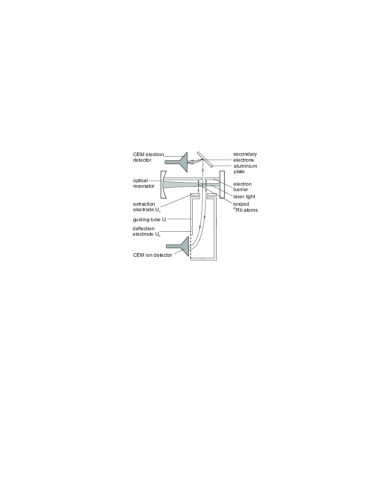
The calibration setup is shown in Fig. 2. Ions are produced by photoionizing 87Rb atoms within a standing wave optical resonator. A commercial rubidium dispenser provides an even rubidium pressure throughout the vacuum chamber containing the apparatus. The background pressure, measured with an ion gauge, is mbar. The optical resonator is located adjacent to the ion optics with its optical axis parallel to the extraction electrode. The resonator is comprised of a flat mirror and a curved mirror (18 mm radius of curvature) separated by 12 mm, resulting in a Gaussian fundamental mode with a beam radius of 46 m. Laser light is coupled into the resonator through the flat mirror with an incoupling efficiency of 80%. The light is taken from a cw single mode diode laser system with a wavelength of 778.1066 nm, resonant to the 5S 5D5/2 transition of 87Rb. We observe a finesse of around 250 and a circulating power of up to 1.5 W within the resonator. The cavity is electronically locked to the side of the resonance peak by controlling the mirror separation with a piezo element. The cavity, including the two mirrors, is shielded from stray electric fields (in particular from the piezo element).
Rubidium atoms that enter the resonator mode are excited from the 5S1/2 to the 5D5/2 state by two photon absorption which is resonantly enhanced by the 5P3/2 state. The transition is Doppler free such that the atoms are excited independent of their velocity. Under these conditions, the transition, which has a natural linewidth below 500 kHz nez1993 , saturates for circulating power greater than 5 mW. The population of the 5D5/2 state is ionized by absorbing a third photon from the resonator mode. The ionization rate is far from saturated due to the short amount of time the atoms spend in the laser field. Together with the strong saturation of the two photon transition, this guarantees that the ionization rate grows linearly with the local intensity. Consequently, the number of generated ions is constant along the axis of the resonator and depends linearly on the circulating power.
A grounded barrier, simulating the atom chip, is located on the other side of the cavity mode from the ion optics. Electrons from the ion detection region pass through the barrier via a 0.5 mm diameter aperture. The fact that this aperture is smaller than the ion extraction aperture, together with the straight field lines between the barrier and the ion extraction electrode, ensure that no electrons from outside the ion detection region are detected, preserving the validity of Eq. 1. The electrons that pass through the aperture impact a grounded aluminium plate, from which secondary electrons are detected with a second CEM with a horn voltage of 300 V. The detection of secondary electrons was necessary due to space limitations preventing mounting the CEM directly adjacent to the aperture.
IV Results
IV.1 Optimization of electrode voltages
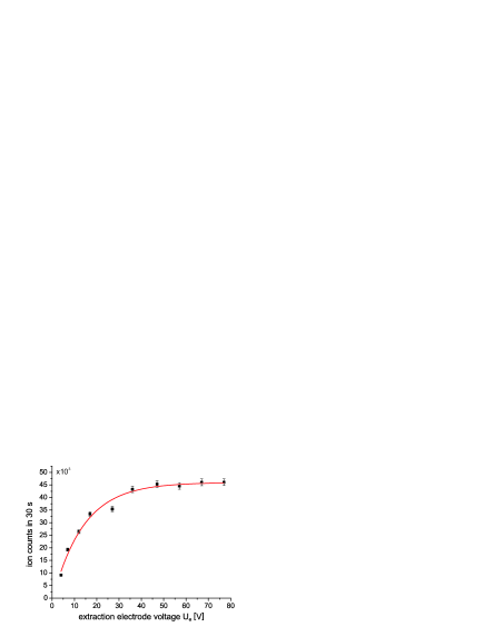
The ion optics electrode voltages were optimized in order to maximize the ion detection rate. For a given value of the extraction electrode voltage , the tube voltage and the deflection electrode voltage were independently varied and the resulting ion detection rate was measured. The maximized ion detection rate is plotted in Fig. 3 as a function of , with and optimized. Since the ion optics contain only electrostatic elements, in the absence of stray fields the ion trajectories, and hence ion detection rate, depend only on the ratios of the electrode voltages. In Fig. 3 the ion detection rate shows an initial increase, followed by a leveling off for values of greater than about 40 V. This indicates that below this voltage, stray fields in the ionization region reduce the detection rate.
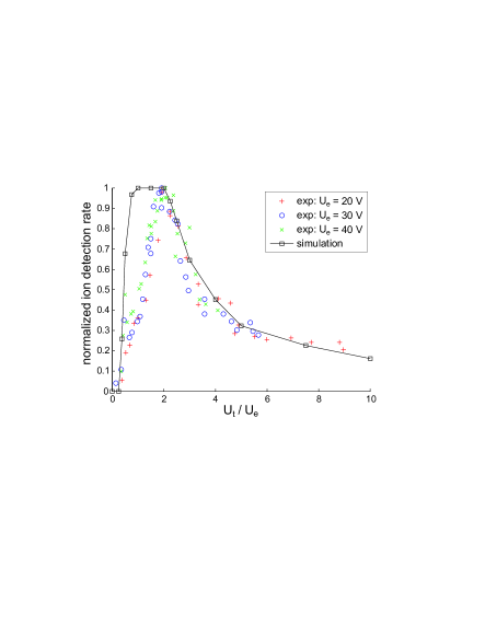
Fig. 4 shows the normalized ion detection rate as a function of the ratio , which determines the focal length of the ion lens. The deflection voltage was optimized for each value of . Experimental results are shown for three different values of and show good agreement with each other, consistent with the fact that the normalized ion detection rate depends on the ratios between the electrode voltages, and not on their absolute values. The curve predicted from the simulation is also shown, and agrees broadly with the experimental results. The difference for low values of is probably due to small variations between the actual and the simulated geometry. In particular, due to the fact that the atoms are ionized less than 1 mm from the electron barrier, the ion trajectories are very sensitive to the position of the hole in the electron barrier relative to the ion optics.
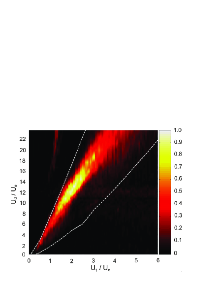
The full dependence of the normalized detection efficiency on the ratios between the electrode voltages is shown in Fig. 5. This data is for V, although essentially the same dependence was observed for other voltages. A non-zero count rate is obtained for relatively large variations in and from their optimal values. Also shown on the plot is the region for which ions impact the CEM, as predicted by numerical simulations. The large region of non-zero count rate and the good agreement between the simulations and experiment means that it is straightforward to set the electrode voltages to values that produce an ion signal. This is an important consideration in setting up an on-chip experiment, in which ions are produced by ionizing atoms from a BEC. This represents a pulsed source with relatively small ion numbers, in contrast to the current situation in which ions are produced by a high flux continuous source.
IV.2 Coincidence spectrum
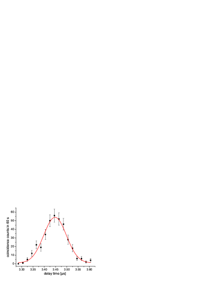
Due to the low mass to charge ratio of electrons relative to the ions, following the ionization of an atom, the electron is detected before the ion. Coincidences were therefore detected by using the electron pulses to trigger a time window for the detection of ion pulses. In order to define this window, it was necessary to measure the coincidence spectrum for the delay times between ions and electrons. This was done by counting the ions arriving within a narrow time window (of width 20 ns) triggered by each electron pulse and following a certain delay time. For a given delay time, the number of ions detected in the 20 ns window was counted over 60 s. By scanning the delay time of the window, the coincidence spectrum was generated (Fig. 6). A peak of true coincidence is observed against a background of false coincidences. The mean delay time given by a Gaussian fit was 3.45 s and the standard deviation was 50 ns. Within the calibration experiments, coincidences were counted using an 800 ns window centered on the peak of the coincidence spectrum.
IV.3 Ion detection efficiency
To measure the efficiency of the ion detector, calibration experiments were carried out with optimized voltages of the ion optics electrodes. In each experiment the numbers of electrons and coincidences were counted in periods of 100 s. The average number of background electrons was measured in separate 100 s periods with the laser detuned 44 GHz off-resonance. The average number of false coincidences was measured by counting the number of coincidences in 100 s periods, with the coincidence window displaced 4 s from the peak of the coincidence spectrum. For our system, the dead time following the detection of a pulse is of order 50 ns, which for the count rates used has a negligible impact on the measured ion detection efficiency.
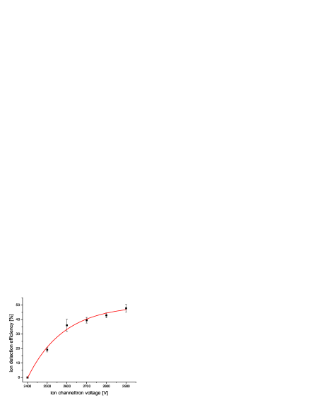
The ion detection efficiency was measured as a function of the voltage across the CEM. For each voltage, several calibration experiments were carried out and the ion detection efficiency for each experiment was calculated from Eq. 1. The curve of the ion detection efficiency was observed to saturate near 50% (Fig. 7). The highest voltage at which we measured the ion detection efficiency was limited by the CEM specifications to 2900 V. At this voltage, the mean value of the ion detection efficiency was and the standard deviation was .
V Discussion
The efficiency of our detector lies at the threshold of the regime in which sub-Poissonian counting is possible. The ion detection efficiency we measured is valid for ions originating from the region from which electrons were also detected. This is due to the fact that only ions correlated with detected electrons were counted in the calibration experiments. According to our ion optics simulations, all the ions from this region are guided to the CEM. Therefore, apart from transmission through the mesh in front of the CEM, the collection efficiency of the ion optics is not a limiting factor in the overall ion detection efficiency. The overall efficiency is then limited by the efficiency of the CEM. This is mainly due to secondary electron emission within the CEM. The number of secondary electrons emitted by an ion impact is approximately described by a Poisson distribution dietz1975 . With the ion energies and CEM material used here, there is a significant probability that no secondary electrons result from an ion impact, or that the electron cascade dies out in the channel. The efficiency could be increased by using a conversion dynode made of a material with a high secondary electron emission coefficient and set to a high voltage. Efficiencies close to 100% may be achieved in principle dietz1975 . However, the required voltages of order 10 kV present a technical challenge in regards to their implementation in an atom chip setup.
In addition to a high detection efficiency, sub-Poissonian atom counting requires low uncertainty in the detection efficiency campey2006a . This uncertainty can result from a lack of knowledge of the detection efficiency, due to the binomial statistics involved in the calibration, and from technical fluctuations. The uncertainty of the ion detection efficiency due to the binomial counting statistics and to the uncertainties in the background electron and false coincidence rates was calculated according to campey2006a and found to be 1.7%. The measured value of 2.6% has an uncertainty of 0.4%, so while it is possible that the fluctuations in the measured values of the detection efficiency result only from the counting statistics, it is likely that technical fluctuations are also present. These fluctuations have a number of possible sources. Variations in the pulse height distribution of the CEM pulses can cause changes in the percentage of the CEM pulses that are above the discriminator level of the pulse counting electronics. Variations in noise on the CEM signals can also change the rate of background counts. Also, the detection efficiency of a CEM depends on the position at which ions impact gilmore1999 . Therefore, noise and drifts in the ion optics electrode voltages which cause small changes in the ion trajectories can introduce further fluctuations.
VI Conclusions
We have presented a detection scheme for single ultracold 87Rb atoms in a magnetic microtrap on an atom chip. In this scheme, the atoms are photoionized on the chip and the resulting ions are guided by ion optics from near the chip surface to a CEM. Using a low vacuum test chamber we were able to optimize and characterize the detector. In this setup the atoms were ionized in a cavity and the ions were collected by the ion optics. By using an additional CEM to count electrons, and by counting electron-ion coincidences with the ion CEM, we were able to measure an ion detection efficiency of 47.8 2.6%. This high detection efficiency make this detector suitable for use in single atom on-chip interferometry and allows the measurement of atom number correlations.
An additional feature of this detector is that when used with pulsed ionization it represents a time of flight mass spectrometer Wiley1955 . The detector has sufficient time resolution to distinguish between ultracold atoms and molecules sdkraft2006 , and thus would prove useful for experiments involving mixtures of different species on atom chips.
From our ion optics simulations, the ion detection efficiency is mainly limited by the efficiency of the CEM. Further improvements can therefore be made by using a conversion dynode for signal amplification. Despite the additional technical challenges this presents, with such an improvement atom counting with sub-Poissonian uncertainty and atom number squeezing experiments are feasible campey2006a . This, together with the detector’s high single atom detection efficiency and high spatial resolution, makes it a sophisticated tool for probing degenerate quantum gases with small particle numbers on atom chips, and allows the investigation of physics beyond the mean field approximation.
VII Acknowledgements
This work was supported by the Landesstiftung Baden-Württemberg through the project “Atomoptik”, by the European Commission through the Marie-Curie Research Training Network “Atom Chips” (MRTN-CT-2003-505032) and by the Australian Research Council. We acknowledge helpful discussions with Herwig Ott and Sebastian Slama.
References
- (1) M. Greiner, O. Mandel, T. Esslinger, T.W. Hänsch and I. Bloch, Nature 415, 39 (2002)
- (2) M. Greiner, O. Mandel, T.W. Hänsch and I. Bloch, Nature 419, 51 (2002)
- (3) C.-S. Chuu, F. Schreck, T. P. Meyrath, J. L. Hanssen, G. N. Price, and M. G. Raizen, Phys. Rev. Lett. 95, 260403 (2005)
- (4) G.B. Jo, Y. Shin, S. Will, T.A. Pasquini, M. Saba, W. Ketterle, D.E. Pritchard, M. Vengalattore, M. Prentiss, arXiv.org, cond-mat/0608585 (2006)
- (5) W. Li, A.K. Tuchman, H.-C. Chien, and M. A. Kasevich, Phys. Rev. Lett. 98, 040402 (2007)
- (6) B. Paredes, A. Widera, V. Murg, O. Mandel, S. Fölling, I. Cirac, G.V. Shlyapnikov, T.W. Hänsch and I. Bloch, Nature 429, 277 (2004)
- (7) T. Kinoshita, T. Wenger and D.S. Weiss, Science 305, 1125 (2004)
- (8) J. Voit, Rep. Prog. Phys. 58, 977 (1995)
- (9) W. Wonneberger, Phys. Lett. A 356, 272 (2006)
- (10) J. Fortágh and C. Zimmermann, Rev. Mod. Phys. 79, 235 (2007)
- (11) T. Schumm, S. Hofferberth, L.M. Anderson, S. Wildermuth, S. Groth, I. Bar-Joeseph, J. Schmiedmayer and P. Krüger, Nature Physics 1, 57 (2005)
- (12) Y.-J. Wang et al., Phys. Rev. Lett. 94, 090405 (2005)
- (13) A. Günther, S. Kraft, C. Zimmermann and J. Fortágh, arXiv.org, cond-mat/0603631 (2006)
- (14) S. Wildermuth, S. Hofferberth, I. Lesanovsky, E. Haller, M. Andersson, S. Groth, I. Bar-Joseph, P. Krüger and J. Schmiedmayer, Nature 435, 440 (2005)
- (15) A. Günther, M. Kemmler, S. Kraft, C. J. Vale, C. Zimmermann and J. Fortágh, Phys. Rev. A 71, 063619 (2005)
- (16) G. Birkl and J. Fortágh, Las. Phot. Rev. 1, 1-12 (2007)
- (17) J. Fortágh, H. Ott, S. Kraft, A. Günther and C. Zimmermann, Appl. Phys. B 76, 157 (2003)
- (18) P.W.H. Pinkse, T. Fischer, P. Maunz and G. Rempe, Nature 404, 365 (2000)
- (19) J.M. Raimond, M. Brune and S. Haroche, Rev. Mod. Phys. 73, 565 (2001)
- (20) M. Schellekens, R. Hoppeler, A. Perrin, J. Viana Gomes, D. Boiron, A. Aspect and C.I. Westbrook, Science 310, 648 (2005)
- (21) T. Jeltes, J.M. Mcnamara, W. Hogervorst, W. Vassen, V. Krachmalnicoff, M. Schellekens, A. Perrin, H. Chang, D. Boiron, A. Aspect and C.I. Westbrook, arXiv.org, cond-mat/0612278 (2006)
- (22) T. Bourdel, T. Donner, S. Ritter, A. Öttl, M. Köhl and T. Esslinger, Phys. Rev. A 73, 043602 (2006)
- (23) I. Teper, Y. Lin and V. Vuletić, Phys. Rev. Lett. 97, 023002 (2006)
- (24) P. Treutlein, T. Steinmetz, Y. Colombe, B. Lev, P. Hommelhoff, J. Reichel, M. Greiner, O. Mandel, A. Widera, T. Rom, I. Bloch and T.W. Hänsch, arXiv.org, quant-ph/0605163 (2006)
- (25) S. Kraft, A. Günther, J. Fortágh and C. Zimmermann, arXiv.org, cond-mat/0702216 (2007)
- (26) T. Campey, C. J. Vale, M. J. Davis, N. R. Heckenberg, H. Rubinsztein-Dunlop, S. Kraft, C. Zimmermann, and J. Fortágh, Phys. Rev. A 74, 043612 (2006)
- (27) Burle Channeltron, model 4502
- (28) SRS Gated Photon Counter, model SR400
- (29) NCRP Report 58, A Handbook of Radioactivity Measurements Procedures, second ed., 76 (1985).
- (30) F. Nez, F. Biraben, R. Felber and Y. Millerioux Opt. Comm. 102, 432 (1993).
- (31) L.A. Dietz and J.C. Sheffield, J. Appl. Phys. 46, 4361 (1975)
- (32) I.S. Gilmore and M.P. Seah, App. Surf. Sci. 144-145, 113 (1999)
- (33) W.C. Wiley and I.H. McLaren, Rev. Sci. Instr. 26, p 1150 (1955)
- (34) S.D. Kraft, P. Staanum, J. Lange, L. Vogel, R. Wester and M. Weidemüller, J. Phys. B 39 S993-S1000 (2006)