Genetic Optimization of Photonic Bandgap Structures
Joel Goh, Ilya Fushman, Dirk Englund, Jelena Vučković
Ginzton Laboratory, Stanford University, Stanford, CA 94305, USA
joelgoh@stanfordalumni.org; ifushman@stanford.edu; englund@stanford.edu; jela@stanford.edu
Abstract
We investigate the use of a Genetic Algorithm (GA) to design a set of photonic crystals (PCs) in one and two dimensions. Our flexible design methodology allows us to optimize PC structures which are optimized for specific objectives. In this paper, we report the results of several such GA-based PC optimizations. We show that the GA performs well even in very complex design spaces, and therefore has great potential for use as a robust design tool in present and future applications.
OCIS codes: (130) Integrated optics; (130.2790) Guided waves; (130.3210) Integrated optics devices; (140) Lasers and laser optics; (140.3410) Laser resonators; (140.5960) Semiconductor lasers; (230) Optical devices; (230.5750) Resonators; (230.6080) Sources; (250) Optoelectronics; (250.5300) Photonic integrated circuits; (260) Physical optics; (260.5740) Resonance;
References and links
- [1] Sajeev John. Strong localization of photons in certain disordered dielectric superlattices. Phys. Rev. Lett., 58(23):2486–2489, Jun 1987.
- [2] Eli Yablonovitch. Inhibited spontaneous emission in solid-state physics and electronics. Phys. Rev. Lett., 58(20):2059–2062, May 1987.
- [3] Dirk Englund, David Fattal, Edo Waks, Glenn Solomon, Bingyang Zhang, Toshihiro Nakaoka, Yasuhiko Arakawa, Yoshihisa Yamamoto, and Jelena Vučković. Controlling the spontaneous emission rate of single quantum dots in a two-dimensional photonic crystal. Phys. Rev. Lett., 95(013904), July 2005.
- [4] Misha Boroditsky, Rutger Vrijen, Thomas Krauss, Roberto Coccioli, Raj Bhat, and Eli Yablonovitch. Control of spontaneous emission in photonic crystals. Proceedings of SPIE - The International Society for Optical Engineering, 3621:190–197, 1999.
- [5] Hatice Altug and Jelena Vučković. Experimental demonstration of the slow group velocity of light in two-dimensional coupled photonic crystal microcavity arrays. Applied Phys. Lett., 86(111102), March 2005.
- [6] Yurii A. Vlasov, Martin O’Boyle, Hendrik F. Hamann, and Sharee J. McNab. Active control of slow light on a chip with photonic crystal waveguides. Nature, 438:65–69, November 2005.
- [7] Hatice Altug and Jelena Vučković. Photonic crystal nanocavity array laser. Opt. Express, 13:8819 – 8828, October 2005.
- [8] Bong-Shik Song, Susumu Noda, Takashi Asano, and Yoshihiro Akahane. Ultra-high-Q photonic double-heterostructure nanocavity. Nature Materials, 4:207–210, 2005.
- [9] Jelena Vučković, Marko Lončar, Hideo Mabuchi, and Axel Scherer. Design of photonic crystal microcavities for cavity QED. Phys. Rev. E, 65(1):016608, Dec 2001.
- [10] Dirk Englund, Ilya Fushman, and Jelena Vučković. General recipe for designing photonic crystal cavities. Opt. Express, 13:5961–5975, August 2005.
- [11] David A.B. Miller Yang Jiao, Shanhui Fan. Demonstration of systematic photonic crystal device design and optimization by low-rank adjustments: an extremely compact mode separator. Opt. Lett., 30:141–143, 2005.
- [12] Stefan Preble, Hod Lipson, and Michal Lipson. Two-dimensional photonic crystals designed by evolutionary algorithms. Applied Phys. Lett., 86(061111), 2005.
- [13] Robert P. Drupp, Jeremy A. Bossard, Douglas H. Werner, and Theresa S. Mayer. Single-layer multiband infrared metallodielectric photonic crystals designed by genetic algorithm optimization. Applied Phys. Lett., 86, Feb 2005.
- [14] J. H. Holland. Adaptation in Natural and Artificial Systems: An Introductory Analysis with Applications to Biology, Control and Artificial Intelligence. Univ. of Michigan Press, 1975.
- [15] D. E. Goldberg. Genetic Algorithms in Search, Optimization and Machine Learning. Addison Wesley, 1989.
- [16] L. Davis. Genetic Algorithms and Simulated Annealing. Morgan Kaufmann, 1987.
- [17] Linfang Shen, Zhuo Ye, and Sailing He. Design of two-dimensional photonic crystals with large absolute band gaps using a genetic algorithm. Phys. Rev. B, 68(035109), 2003.
- [18] E. Kerrinckx, L. Bigot, M. Douay, and Y. Quiquempois. Photonic crystal fiber design by means of a genetic algorithm. Opt. Express, 12, May 2004.
- [19] Steven G. Johnson and J. D. Joannopoulos. Block-iterative frequency-domain methods for maxwell’s equations in a planewave basis. Opt. Express, 8(3):173–190, 2001.
- [20] Yoshihiro Akahane, Takashi Asano, Bong-Shik Song, and Susumu Noda. High-Q photonic nanocavity in a two-dimensional photonic crystal. Nature, 425:944–947, 2003.
- [21] P. Lalanne, S. Mias, and J. Hugonin. Two physical mechanisms for boosting the quality factor to cavity volume ratio of photonic crystal microcavities. Opt. Express, 12:458–467, Feb 2004.
- [22] A. Yariv and P. Yeh. Optical Waves in Crystals: Propagation and Control of Laser Radiation. John Wiley and Sons Inc, 2002.
1 Introduction
Photonic crystals (PCs) describe a class of semiconductor structures which exhibit a periodic variation of refractive index in 1, 2, or 3 dimensions. As a result of this periodic variation, PCs possess a photonic band gap – a range of frequencies in which the propagation of light is forbidden [1, 2]. This is the analog of the electronic bandgap in traditional semiconductors. This unique characteristic of PCs enables them to be used to effectively manipulate light. PCs have already been used for applications such as modifying the spontaneous emission rate of emitters [3, 4], slowing down the group velocity of light [5, 6], and designing highly efficient nanoscale lasers [7].
Given that Photonic Crystals find applications in a myriad of areas, we proceed to investigate the question: What is the best possible PC design for a given application? Traditionally, the design of optimal PC structures has been largely done by either trial-and-error, iterative searches through a design space, by physical intuition, or some combination of the above methods [8, 9]. However, such methods of design have their limitations, and recent developments in PC design optimization have instead taken on a more systematic and algorithmic nature [10, 11, 12, 13]. In this work, we report the results of a Genetic Algorithm to optimize the design of a set of one and two-dimensional PC structures. We show that the Genetic Algorithm can effectively optimize PC structures for any given design objective, and is thus a highly robust and useful design tool.
2 Genetic Algorithms
Genetic Algorithms (also known as Evolutionary Algorithms) are a class of optimization algorithms that apply principles of natural evolution to optimize a given objective [14, 15, 16]. In the genetic optimization of a problem, different solutions to the problem are picked (usually randomly), and a measure of fitness is assigned to each solution. On a given generation of the design, a set of operations, analogous to mutation and reproduction in natural selection, are performed on these solutions to create a new generation of solutions, which should theoretically be “fitter” than their parents. This process is repeated until the algorithm terminates, typically after a pre-defined number of generations, or after a particularly “fit” solution is found, or more generally, when a generation of solutions meets some pre-defined convergence criterion.
3 Implementation
Genetic Algorithms have already been used in PC design - to find non-intuitive large-bandgap designs [12, 17] and for designing PC fibers [18]. In our work, we performed the genetic optimization by varying the sizes of circular holes in a triangular lattice. This approach was chosen because the search space is conveniently constrained in this paradigm, and the optimized structures can be easily fabricated, if desired. A freely available software package [19] was used to simulate the designed structures.
In addition, we used the following parameters for the implementation of our Genetic Algorithm:
-
Chromosome Encoding. We used a direct-chromosome encoding, where the various optimization parameters were stored in a vector. For the current simulations, for simplicity, we only varied the radii of cylindrical holes in a triangular lattice. Our implementation can be easily modified to include other optimization parameters as well, such as the positions of the various holes, or the refractive index of the dielectric material.
-
Selection. We used fitness-proportionate selection (also known as roulette-wheel selection), to choose parent chromosomes for mating. In this selection scheme, a chromosome is selected with a probability that is proportional to its fitness , as shown in Eq. (1).
(1) -
Mating. After a pair of parent chromosomes and were selected, they were mated to produce a child chromosome by taking a random convex combination of the parent vectors, as in Eq. (3).
(2) -
Mutation. Mutation was used to introduce diversity in the population. We used two types of mutation in our simulations, a random-point crossover and a gaussian mutation.
1) Random-point crossover: For an original chromosome vector of length , we select a random index, , from 0 to as the crossover point, and swap the two halves of to produce the mutated vector, , as represented in Eq. (3).
(3) 2) Gaussian mutation: To mutate a chromosome vector by Gaussian mutation, we define each element of to be independent and identically distributed Gaussian Random Variables with mean and a standard deviation proportional to the corresponding elements of . This searches the space in the vicinity of the original chromosome vector .
(4) is a algorithm-specific variance, and can be tuned to change the extent of parameter-space exploration due to mutation.
-
Cloning. To ensure that the maximum fitness of the population was would never decrease, we copied (cloned) the top few chromosomes with the highest fitness in each generation and inserted them into the next generation.
4 Simulation Results
4.1 Optimizing Planar Photonic Cavity Cavities
4.1.1 Q-factor Maximization
One problem of interest in PC design is the inverse problem, where one tries to find a dielectric structure to confine a given (target) electromagnetic mode. Here we consider the inverse design problem of optimizing a linear-defect cavity in a planar photonic crystal cavity. The Q-factor is a common figure of merit measuring how well a cavity can confine a given mode, and can be approximated (assuming no material absorption) by the following expression:
| (5) |
where represents the Q-factor in the direction parallel to the slab, and represents the Q-factor perpendicular to the slab. is usually the limiting factor for . As was shown previously [10, 20], the vertical mode confinement, which occurs through total internal reflection (TIR), can be improved if the mode has minimal k-space components inside the light cone.
In the subsequent sections, we report the results where we employed our GA to minimize the light cone radiation of such cavities. We used one-dimensional photonic crystals as approximations to these cavities [21], and simulated these cavities using the standard Transfer Matrix method for the E-field [22].
4.1.2 Matching to a Target Function
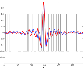
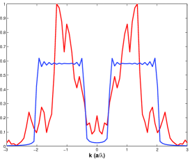
In [10] it was noted that minimization of light cone radiation could be performed via mode-matching to a target function which already possessed such a property. We therefore used a fitness function that was equal (up to a normalizing factor) to the reciprocal of the mean-squared difference between our simulated mode and a target mode (see Eq (6)). For this simulation, our chromosome encoded the thicknesses of the dielectric slabs in the structure, and was a vector of length 10. We used 100 chromosomes in each generation and allowed them to evolve for 80 generations.
| (6) |
We used target modes that were sinusoidal functions multiplied by sinc and sinc-squared envelope respectively. Such target modes have theoretically no radiation at or near the Gamma point and are therefore ideal candidates as target functions. The results, shown in Fig. 1, clearly feature a suppression of k-vector components at low spatial-frequencies. Matching using the the sinc-squared envelope target function appeared to produce a better match. From the k-space plots, the GA evidently had difficulty matching the sharp edges for the sinc-envelope target mode.
4.1.3 Direct Minimization of Light Cone Radiation
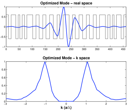
In the preceding subsection, we observed that when we formulated our objective as a matching problem, in the case of the sinc-envelope, the GA sacrificed the desired low spatial-frequency suppression in an effort to match the overall shape of the function. The preceding formulation therefore poses an implicit constraint on our optimization. By reformulating the optimization problem, we were able to effectively remove this constraint, and obtain a better result.
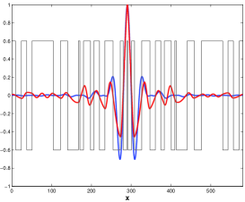
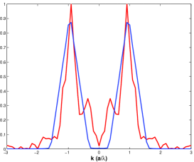
Our reformulation directly minimized the k-vector components in the light cone, by minimizing the integrated square-magnitude of the simulated E-field mode in k-space inside the light cone. The fitness function that we used is given as in Eq (7), where V represents the set of k-vectors within the light cone.
| (7) |
The final, evolved structure, together with the corresponding real-space and k-space mode profiles are shown in Fig 2. The k-space mode profile features a strong suppression of radiation at low frequencies, to a greater extent as compared to the optimized fields from the preceding simulations. By relaxing our constraint and performing a direct optimization, our GA has designed a structure that achieves better light cone suppression than before. Our direct optimization paradigm has exploited the extreme generality of the GA, which simply requires that a fitness function be defined, with little further constraint thereafter.
4.2 Maximal Gap at any k-vector Point
Moving on to the more generic case of 2D photonic crystals, we will proceed to show the results of simulations for maximizing the TE bandgap at any point in k-space for a 2-Dimensional PC structure with a triangular lattice of air holes. This could be useful for PC design applications where the target mode to be confined is centered around a particular point in k-space [10]. By maximizing the bandgap at that k-space point, we would effectively design a better mirror for a mode resonating along this k-space direction.
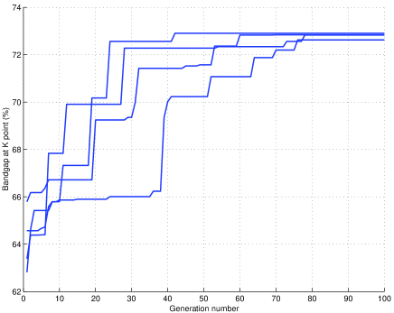
We used a supercell which was three periods wide in each dimension and varied the radii of the nine holes in total, and we encoded the chromosome as a vector of these nine holes. We used a population size of 60 chromosomes for each generation, and allowed the optimization to run for a total of 100 generations.
To evaluate the fitness of each chromosome, we used the eigensolver in Ref [19] to calculate the gap-to-midgap ratio at the K-point of the band diagram. We then scaled the calculated ratio exponentially to tune the selection pressure of the optimization. Figure 3 shows the variation of the gap-to-midgap ratio of our structures as the algorithm progressed.
Our Genetic Algorithm performs as expected, and we get a general increase of fitness as the algorithm progresses. All the four runs do not show any significant increase in fitness after Generation 80, at which point they have maximum fitnesses (i.e. ratio of their bandgap to midgap value) of around 72%. All the optimized structures after the run have similar dielectric structures and band diagrams. The dielectric structures and a sample band diagram is shown in Figure 4.
4.3 Optimal dual PC structures
As a more complex example, let us consider two similar PC designs, (1) a triangular lattice of air holes in a dielectric slab, and (2) a triangular lattice of dielectric rods in air. Structure (1) possesses a bandgap for TE light, but no bandgap for TM light, while structure (2) possesses a bandgap for TM light, but not for TE light.
Our objective is to use the Genetic Algorithm to find a PC design in which the TE eigenmode for structure (1) and the TM eigenmode for structure (2) are most similar. Maxwell’s equations can be cast as eigenproblems for the Electric or Magnetic fields, and our approach could be potentially useful in future PC design, because solving the inverse problem is analytically simpler (at least intuitively) for the eigenproblem involving the E-field.
We used a 3x3 supercell for the optimization, and we minimize the mean-square difference of the z-components of the electric and magnetic fields of the dual structures at the K-point of the band diagram. We recognize a priori that a trivial solution, which we wish to avoid, is a structure that has a uniform refractive index (either dielectric or air) throughout, and so we prevent the genetic algorithm from obtaining this by restricting our mutation to only a Gaussian mutation (see Eq. 4). This preferentially searches the locality of points, and is a necessary trade-off for obtaining a reasonable solution. This illustrates the versatility of the Genetic approach - the extent of the search can be easily modified by a simple change of algorithm parameters. Fig. 5 shows the optimal dual structures with the corresponding simulated fields.
5 Conclusion
From the results above, we have shown that our Genetic Algorithm is able to effectively optimize PC designs to meet specific design criteria. Furthermore, by our choice of encoding, we could easily impose constraints upon the design space to ensure that every design searched by the algorithm could be realistically fabricated. Between different optimizations, all that needed to be changed was the measure of how well a given structure complied with our design criterion - the ”fitness function” in Genetic Algorithm parlance. Our Genetic Algorithm is therefore highly robust and can be easily modified to optimize any user-defined objective function.