Present address: ]Van der Waals-Zeeman Instituut, Universiteit van Amsterdam, Valckenierstraat 65-67, 1018 XE Amsterdam, The Netherlands
Scanning magnetoresistance microscopy of atom chips
Abstract
Surface based geometries of microfabricated wires or patterned magnetic films can be used to magnetically trap and manipulate ultracold neutral atoms or Bose-Einstein condensates. We investigate the magnetic properties of such atom chips using a scanning magnetoresistive (MR) microscope with high spatial resolution and high field sensitivity. We show that MR sensors are ideally suited to observe small variations of the magnetic field caused by imperfections in the wires or magnetic materials which ultimately lead to fragmentation of ultracold atom clouds. Measurements are also provided for the magnetic field produced by a thin current-carrying wire with small geometric modulations along the edge. Comparisons of our measurements with a full numeric calculation of the current flow in the wire and the subsequent magnetic field show excellent agreement. Our results highlight the use of scanning MR microscopy as a convenient and powerful technique for precisely characterizing the magnetic fields produced near the surface of atom chips.
pacs:
39.25.+k,07.55.GeI Introduction
Surface based potentials for manipulating neutral atoms on a micron scale have attracted widespread interest in recent years. Atom chips Folman et al. (2002); Fortágh and Zimmermann (2007) consisting of planar geometries of microfabricated wires or patterned magnetic materials provide intricate magnetic potentials and have become a practical and robust tool for producing, trapping and manipulating Bose-Einstein condensates. Atoms chips have recently been used to precisely position Bose-Einstein condensates Günther et al. (2005), realize trapped atom interferometers Schumm et al. (2005); Jo et al. (2007) and have provided new and sensitive techniques for detecting tiny forces on a small spatial scale Hall et al. (2007). The fabricated wires or magnetic materials used for atom chips have been the topic of several recent studies, finding that their quality must be exceptionally high since even the smallest imperfections, for example roughness of the wire edge, can lead to uncontrolled magnetic field variations. These variations subsequently corrugate the bottom of the trapping potential Wang et al. (2004); Estève et al. (2004). Recently, fragmentation of ultracold atoms has also been observed in close proximity to magnetic materials Sinclair et al. (2005); Whitlock et al. (2007a); Boyd et al. (2006) and has been traced to long range spatial variations in the film magnetization Whitlock et al. (2007a). As the energy scales associated with ultracold atoms and Bose-Einstein condensates are in the nanokelvin regime, even the smallest magnetic field variations of only a few nanotesla can dramatically alter their properties Wildermuth et al. (2005).
Until now, characterizing the smoothness of the potentials produced by atom chips has relied on the atom clouds themselves, through either the equilibrium atomic density distribution Estève et al. (2004) or radio frequency spectroscopy of trapped atom clouds Whitlock et al. (2007a). With the increasing complexity of atom chips, however, it is necessary to obtain fast and reliable methods of characterizing the magnetic potentials prior to installing the atom chips in ultrahigh vacuum and trapping ultracold atoms.
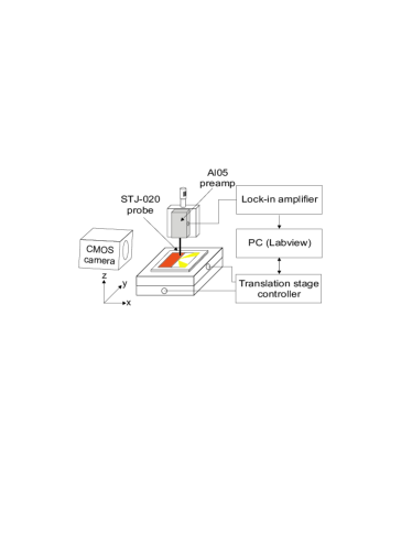
In this paper we describe the application of a micron sized magnetoresistance (MR) sensor to accurately profile the magnetic fields generated by magnetic film and current-carrying wire atom chips. Our home-built magnetoresistance microscope (Fig. 1) is used to measure small magnetic field variations above a permanent magnetic film atom chip which causes fragmentation of ultracold atom clouds. The MR measurements support independent measurements performed using trapped ultracold atoms as the magnetic field probe Whitlock et al. (2007a). The study indicates the variations occur predominately near the edge of the film and are associated with heating of the film during vacuum bake-out. In addition, we have fabricated a new current-carrying wire atom chip using femtosecond laser ablation of a gold film Whitlock et al. (2007b). A wire is sculpted with a periodically modulated edge to produce a complex magnetic potential for ultracold atoms. Two dimensional images of the field produced by the wire are obtained and are in excellent agreement with numeric calculations of the expected field strength. The measurements show that it is possible to fabricate and characterize a linear array of magnetic potentials produced by modifying the edge of a straight current carrying wire.
II Apparatus
Analysis of the atom chips is performed using an ultra-sensitive low-field magnetoresistive sensor based on magnetic tunneling junction technology Moodera et al. (1995); Lacoura et al. (2002). A magnetic tunneling junction sensor consists of two ferromagnetic layers separated by an ultra-thin insulating interlayer. One magnetic layer has fixed ‘pinned’ magnetization while the other responds to the local magnetic field. The interlayer resistance depends on the relative magnetization of the neighboring magnetic layers. These devices provide an absolute measure of the magnetic field with high sensitivity and high spatial resolution. They provide a linear response over a large field range (typically about 0.5 mT) and are ideal for studying the magnetic fields produced by microfabricated current-carrying wires or patterned magnetic materials on atom chips. Here the sensor is incorporated into a home-built scanning magnetic field microscope, schematically depicted in Figure 1, and used to study the corrugated field produced by the atom chip.
The microscope (Fig. 1) consists of the MR sensor probe, the preamplification electronics, a lock-in amplifier, a motorized x-y translation stage and a computer interfaced via LabView to both stage and lock-in amplifier. The probe tip is manually positioned above the sample using a micrometer stage and a CMOS camera for height calibration. This setup allows us to acquire one-dimensional scans as well as two-dimensional maps of the -component, i.e. the out-of-plane component, of the magnetic field at variable heights above the sample surface.
Our scanning magnetoresistance microscope incorporates a commercially available magnetic tunnel junction probe (MicroMagnetics STJ-020), polished to allow very close approaches to the surface (10 m). The active area of the sensor is approximately m2 and it detects the magnetic field oriented along the sensor tip ( direction). The sensor is interfaced using an Anderson loop Anderson (1992) to convert small changes in the sensor resistance to a signal voltage. The output is then amplified using a signal amplification board (MicroMagnetics AL-05) with a gain of 2500 and a bandwidth of 1 MHz. The sensor and preamplifier are calibrated to give an output of 20 V/mT. Due to its small size the sensor exhibits significant noise which can be overcome by reducing the bandwidth of the output signal.
To increase the signal-to-noise ratio we use an AC modulation technique. In the case of current-carrying wires this is simply done by modulating the wire current at kHz frequencies and detecting the signal with a lock-in amplifier (Stanford Research Systems SR830). When studying permanent magnetic films we use mechanical modulation of the probe. The tip of the probe is oscillated along the scanning direction at its mechanical resonance frequency (18 kHz) using a piezo actuator. At this frequency the noise level of the sensor is reduced to less than 15% compared to DC; however the output of the lock-in amplifier is now proportional to the first derivative of the magnetic field. This output is calibrated against a known magnetic field gradient by first measuring the field in DC mode 200 m above the edge of the film. The field is large enough to provide good signal-to-noise and features a large gradient of 1 Tm-1. We then compare the numerical derivative of this measurement to the data obtained while oscillating the tip. This allows us to determine the oscillation amplitude of the probe and hence to reconstruct the magnetic field up to a constant offset by numerical integration of the data. The oscillation amplitude and subsequently the spatial resolution of this measurement is approximately 50 m. The AC modulation technique reduces the noise levels to about T, equivalent to that obtained using ultracold atoms as a probe Whitlock et al. (2007a) and a factor of 5 lower than what is obtained for an equivalent measurement time using just low-pass filtering.
III Permanent magnet atom chip
As a first application of the magnetic field microscope we investigated the random variations in the magnetic potential created near the surface of a magnetic film atom chip used in previous experiments to trap ultracold atoms and Bose-Einstein condensates and is described in detail elsewhere Hall et al. (2006). It uses a multilayer Tb6Gd10Fe80Co4 film which exhibits strong perpendicular anisotropy. The film is deposited on a 300 m thick glass substrate where one edge is polished to optical quality prior to film deposition. At this edge the magnetic film produces a field that is analogous to that of a thin current-carrying wire aligned with the edge (I = 0.2 A). A magnetic microtrap is formed by the field from the film, a uniform magnetic bias field, and two current-carrying end-wires. To account for the need of a reflecting surface for the mirror magneto-optical trap the chip is completed by a second glass slide and both sides are coated with gold.
Due to their narrow energy distribution, ultracold atoms are very sensitive to small fluctuations of the magnetic trapping potential. In a recent paper Whitlock et al. (2007a) we used radio frequency (rf) spectroscopy of trapped atoms to measure the absolute magnetic field strength above the edge of the film. This provided an accurate measurement of the corrugation of the longitudinal component of the magnetic field produced by the permanent magnetic atom chip, i.e. the component parallel to the film edge. We also developed a model describing the spatial decay of random magnetic fields from the surface due to inhomogeneity in the film magnetization.
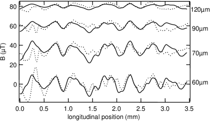
After removing the atom chip from the vacuum chamber we used the magnetoresistance microscope to further characterize the film properties. Our first measurement consists of a series of scans of the magnetic field parallel to the film edge over a region of 3.5 mm at various heights ranging from m down to m, the minimum distance limited by the adjacent protruding gold coated glass slide. Four of these profiles are depicted in Figure 2. Due to the large field gradient produced at the film edge it was necessary to carefully align the measurement direction and subtract a third order polynomial from the data. Also plotted in the same figure are the corresponding profiles previously measured by rf spectroscopy of ultracold atoms. The results from the two different methods are in remarkable agreement. It should be noted however that a quantitative comparison is difficult as the two methods are sensitive to different components of the corrugated magnetic field: the magnetoresistive sensing direction is perpendicular to the surface while the trap bottom probed by the rf spectroscopy is defined by the in-plane component of the magnetic field.
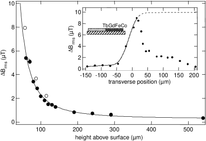
The results of the complete series of magnetoresistance scans as well as the rf spectroscopy measurements are summarized in Figure 3 where the root mean square (rms) noise is plotted as a function of distance to the surface. For random white noise fluctuations of the film magnetization our model described in Whitlock et al. (2007a) predicts a decay of the field roughness. A power law fit to the data obtained by the MR scans gives in excellent agreement with this prediction.
We have also performed a series of scans at constant height (m) above the film surface but variable transverse distance to the film edge. The rms noise levels of these scans are depicted in the inset of Figure 3 (circles) together with the prediction of the random magnetization model (lines). While the model describes the results adequately above the non-magnetic half plane of the atom chip the measured inhomogeneity decreases away from the edge above the magnetic film side, whereas in the case of homogeneous magnetization fluctuations is expected to stay constant (dotted line in Fig. 3).
IV Tailored magnetic microtraps
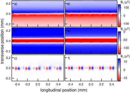
Section III of this paper focused on MR studies of the corrugated potential produced by a partially inhomogeneous magnetic film atom chip. In this section, we describe the analysis of a current-carrying wire atom chip fabricated using micron-scale femtosecond laser ablation of a thin metal film. We have produced a tailored magnetic potential by sculpting the shape of a wire to create a linear array of magnetic traps for cold atoms. Two-dimensional magnetoresistance microscopy provides an image of the perpendicular magnetic field component produced by the wire at a fixed distance to the surface. A solution to the magnetostatic inverse problem is then applied to obtain the remaining two field components, allowing a complete reconstruction of the magnetic trapping potential. Of particular interest is the field component parallel to the wire, which defines the bottom of the trapping potential. A comparison of the measured and reconstructed field components with full numeric calculations of the field produced by the sculptured wire shows excellent agreement.
IV.1 Sculptured wire atom chip
Femtosecond laser ablation can be used to pattern micron and submicron scale structures on a wide variety of materials Nolte et al. (1997) and can be used to produce atom chips Whitlock et al. (2007b). In this work we use the technique to directly fabricate complex wire patterns in an evaporatively deposited gold film to form a current-carrying wire atom chip Fortágh and Zimmermann (2007). The chip consists of a glass slide substrate with a 25 nm thick Cr bonding layer and a 150 nm thick Au layer. The wire structure is patterned by cutting three m wide insulating channels into the Au film.
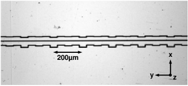
We have patterned two parallel Au wires with widths of 20 and 30 m and lengths of 10 mm which can be used to create a magnetic potential for trapping Bose-Einstein condensates (Fig. 4). Each wire has been sculptured with one periodically modulated boundary with a period of m. Deliberately modulating the wire boundary slightly modifies the current path and produces a small field component oriented parallel to the wire, which modulates the corresponding longitudinal magnetic potential experienced by the trapped atoms Pietra et al. (2005). This is used to realize a linear array of asymmetric double wells which are separated by potential barriers with small amplitudes which can be precisely controlled by varying the wire current or the distance of the trap to the wire surface Schumm et al. (2005); Hall et al. (2007); Sidorov et al. (2006).
The m wire is chosen for the magnetoresistance measurements. We use the reference source of the lock-in amplifier to drive a small AC current of 37 mA rms through the wire at a frequency of 1 kHz. The output of the lock-in amplifier is recorded by a computer. Two computer controlled translations stages are used to position the wire sample with respect to the MR probe. The probe is calibrated against the expected field produced by the wire calculated using Biot-Savart’s law, neglecting the effect of the small modulations. We record an image of the perpendicular magnetic field component produced by the wire over a 21.5 mm2 spatial region at a distance of m above the wire. The spatial resolution is m which corresponds to data points. The lock-in integration time is set to 300 ms and each line of the image is scanned twice and averaged, which results in a measurement time of approximately 5 hours for the whole two-dimensional magnetic field image. Figure 5a shows the result of this measurement (only the central part of the full image is shown). The field amplitude produced across the wire at this height is T. Directly above the wire the perpendicular field is nearly zero apart from a small modulated field component with amplitude of about T. The noise level for this measurement determined from a region about 0.7 mm away from the wire was as low as 50 nT.
IV.2 Reconstruction of the in-plane field components
With a two-dimensional image of the out-of-plane field component at a given height it is possible to convert to a uniquely defined in-plane current distribution Roth et al. (1989) and subsequently back to any other field component. Given that the height of the wire is small compared to the measurement distance above the surface, the current density can be considered as a two-dimensional distribution. The Fourier transforms of the magnetic field components and are then simply related to :
| (1) |
where .
Shown in Figure 5 (b) and (c) are the reconstructed in-plane field components and derived from the measured component. The field image clearly shows the modulated component along the length of the wire which defines the bottom of the trapping potential.
IV.3 Numeric calculations of magnetic fields
We have also performed detailed numeric calculations of the field produced by the sculptured wire to compare them with our measurements. The current density distribution of the wire is computed from the solution of Laplace’s equation satisfied by the electrostatic potential . We assume that the conductivity is uniform throughout the wire and, since we are interested in the field at distances much larger than the wire thickness, we assume that depends only on and . Exact analytical solutions for this problem can be obtained for particular geometries; however in general one has to rely on numerical methods.
Here, solutions of Laplace’s equation were computed using the finite element method which provides an approximate solution of partial differential equations with defined boundary conditions. For this problem we have used the Matlab Partial Differential Equation (PDE) toolbox. The boundary conditions are specified such that the normal component of the current density on the wire edge is zero (Neumann conditions). The wire geometry is then decomposed into a set of triangular elements which define a mesh of nodes, for each of which the electrostatic potential is solved. From this it is straight forward to compute the current distribution and the associated magnetic field. The results of these calculations are depicted in Figure 5 (d) to (f) next to the corresponding measurements.
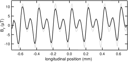
The component of the magnetic field produced by the atom chip is of particular interest because it determines the potential minimum experienced by the trapped atoms. Figure 6 compares field profiles of along the wire extracted from the measurement and the simulation. We note that the two profiles differ by about 10% in amplitude and attribute this to a systematic error in the calibration of the sensor which was done assuming that the measured profile was produced by an infinitely thin wire. In addition to that, the measured field amplitude decreases slightly over the 2 mm scan region which is most likely due to a tilt between the sample surface and the measurement plane on the order of 2 mrad.
V Conclusion
We have demonstrated a scanning magnetic microscopy technique for characterizing atom chips. The microscope is based on a commercially available magnetoresistive probe. It has been used to scan the corrugation of the magnetic field produced by a permanent magnet atom chip as well as to investigate the field produced by a sculptured current-carrying wire.
The spatial resolution of the device is in principle limited by the size of the active area of the probe, i.e., about m for the sensor used in this work; however submicron resolution has been demonstrated in similar applications Schrag and Xiao (2003). For our demonstration the smallest measurable feature sizes were determined by the minimum distance to the surface (m) and the scaling laws for magnetic fields. The scan range is limited only by the computer controlled translation stages which can easily be extended to several centimeters.
By simple low pass filtering of the output signal and averaging we were able to achieve a sensitivity of 0.5 T when measuring a permanent magnetic film. Using AC modulation techniques we could reduce this down to 0.1 T in case of stationary magnetic fields and even 50 nT for current carrying wires.
In conclusion, the high field sensitivity, large scan range, ease of use and low cost makes the magnetoresistance microscope the quintessential tool for ex-situ characterization of cold atom magnetic microtraps.
Acknowledgements.
The authors would like to thank J. Wang for the deposition of the films. This project is supported by the ARC Centre of Excellence for Quantum-Atom Optics.References
- Folman et al. (2002) R. Folman, P. Krüger, J. Schmiedmayer, J. Denschlag, and C. Henkel, Adv. At. Mol. Opt. Phys. 48, 263 (2002).
- Fortágh and Zimmermann (2007) J. Fortágh and C. Zimmermann, Rev. Mod. Phys. 79, 235 (2007).
- Günther et al. (2005) A. Günther, M. Kemmler, S. Kraft, C. J. Vale, C. Zimmermann, and J. Fortágh, Phys. Rev. A 71, 063619 (2005).
- Schumm et al. (2005) T. Schumm, S. Hofferberth, L. M. Andersson, S. Wildermuth, S. Groth, I. Bar-Joseph, J. Schmiedmayer, and P. Krüger, Nature 1, 57 (2005).
- Jo et al. (2007) G.-B. Jo, Y. Shin, S. Will, T. A. Pasquini, M. Saba, W. Ketterle, and D. E. Pritchard, Phys. Rev. Lett. 98, 030407 (2007).
- Hall et al. (2007) B. V. Hall, S. Whitlock, R. Anderson, P. Hannaford, and A. Sidorov, Phys. Rev. Lett. 98, 030402 (2007).
- Wang et al. (2004) D. W. Wang, M. D. Lukin, and E. Demler, Phys. Rev. Lett. 92, 076802 (2004).
- Estève et al. (2004) J. Estève, C. Aussibal, T. Schumm, C. Figl, D. Mailly, I. Bouchoule, C. I. Westbrook, and A. Aspect, Phys. Rev. A 70, 043629 (2004).
- Sinclair et al. (2005) C. D. J. Sinclair, J. A. Retter, E. A. Curtis, B. V. Hall, I. Llorente-Garcia, S. Eriksson, B. E. Sauer, and E. A. Hinds, Eur. Phys. J. D 35, 105 (2005).
- Whitlock et al. (2007a) S. Whitlock, B. V. Hall, T. Roach, R. Anderson, M. Volk, P. Hannaford, and A. I. Sidorov, Phys. Rev. A 75, 043602 (2007a).
- Boyd et al. (2006) M. Boyd, E. W. Streed, P. Medley, G. K. Campbell, J. Mun, W. Ketterle, and D. E. Pritchard, cond-mat/0608370 (2006).
- Wildermuth et al. (2005) S. Wildermuth, S. Hofferberth, I. Lesanovsky, E. Haller, L. M. Andersson, S. Groth, I. Bar-Joseph, P. Krüger, and J. Schmiedmayer, Nature (London) 435, 440 (2005).
- Whitlock et al. (2007b) S. Whitlock et al., unpublished (2007b).
- Moodera et al. (1995) J. S. Moodera, L. R. Kinder, T. M. Wong, and R. Meservey, Phys. Rev. Lett. 74, 3273 (1995).
- Lacoura et al. (2002) D. Lacoura, H. Jaffre’s, F. N. V. Dau, F. Petroff, A. Vaure’s, and J. Humbert, J. Appl. Phys. 91, 4655 (2002).
- Anderson (1992) K. F. Anderson, NASA TM-104260 (1992).
- Hall et al. (2006) B. V. Hall, S. Whitlock, F. Scharnberg, P. Hannaford, and A. Sidorov, J. Phys. B: At. Mol. Opt. Phys. 39, 27 (2006).
- Nolte et al. (1997) S. Nolte, C. Momma, H. Jacobs, A. Tünnermann, B. N. Chichkov, B. Wellegehausen, and H. Welling, J. Opt. Soc. Am. B 14, 2716 (1997).
- Pietra et al. (2005) L. D. Pietra, S. Aigner, C. v. Hagen, H. J. Lezec, and J. Schmiedmayer, J. Phys.: Conf. Ser. 19, 30 (2005).
- Sidorov et al. (2006) A. I. Sidorov, B. J. Dalton, S. M. Whitlock, and F. Scharnberg, Phys. Rev. A 74, 023612 (2006).
- Roth et al. (1989) B. J. Roth, N. G. Sepulveda, and J. P. Wilkswo, J. Appl. Phys. 65, 361 (1989).
- Schrag and Xiao (2003) B. D. Schrag and G. Xiao, Appl. Phys. Lett. 82, 3272 (2003).