Local and Non-local Shot Noise in Multiwalled Carbon Nanotubes
Abstract
We have investigated shot noise in multiterminal, diffusive multiwalled carbon nanotubes (MWNTs) at 4.2 K over the frequency MHz. Quantitative comparison of our data to semiclassical theory, based on non-equilibrium distribution functions, indicates that a major part of the noise is caused by a non-equilibrium state imposed by the contacts. Our data exhibits non-local shot noise across weakly transmitting contacts while a low-impedance contact eliminates such noise almost fully. We obtain for the intrinsic Fano factor of our MWNTs.
pacs:
PACS numbers: 67.57.Fg, 47.32.-yMultiwalled carbon nanotubes (MWNTs) are miniscule systems, their diameter being only a few nanometers. Yet, in surprisingly many cases their transport properties can be described with incoherent theories, interference effects showing up only through weak localization Schonenberger ; Strunk . This is in contrast to single-walled tubes, where interference effects dominate, and give rise for example to Fabry-Perot resonances with distinctive features in conductance and current noise wu07 .
When interference effects are washed out, semiclassical analysis based on non-equilibrium distribution functions is adequate, and the circuit theory of noise becomes a powerful tool in considering nanoscale objects semiclassical ; Nazarov02 . This theory makes it straightforward to calculate current noise of incoherent dots and wires, and to relate the current noise to the transmission properties of the corresponding section of the mesoscopic object. Semiclassical analysis provides a way to make a distinction between sample and contact effects, and thereby it allows one to investigate contact phenomena, of which only a little is known in carbon nanotube systems.
We have investigated the influence of contacts on the shot noise in multiterminal, diffusive carbon nanotubes. We have made four-lead measurements on MWNTs in which two middle probes have been employed for noise measurements. We show that quantitative information can be obtained from such measurements using semiclassical circuit theory in the analysis. We find that probes with contact resistance k act as strongly inelastic probes, resulting in incoherent, classical addition of noise of two adjacent sections, while ”bad” contacts ( k) act as weakly perturbing probes which need to be analysed on the same footing as the other parts of the sample. We also find that good contacts eliminate noise that couples to the probe from a non-neighboring voltage biased section. In addition, we find from our analysis that the tubes themselves are quite noise-free, with a Fano-factor . As far as we know, our results are the first shot noise measurements addressing the contact issues in carbon nanotubes.
To clarify the results of our multi-probe noise measurements, let us consider the three-terminal structure depicted schematically in Fig. 1. Assume that the average current flows between 1 and 2, and the average potential of the terminal 3 adjusts to the potential of the node. In our work, terminal 3 is disconnected from the ground at low frequencies, but at the high frequencies of the noise measurement, the impedance to the ground is much lower than that of the contacts. As a result, the effect of voltage fluctuations in the third terminal on the overall noise can be neglected. We describe two kinds of noise measurements: “local”, where the noise is measured from one of the terminals 1 or 2, and “nonlocal”, where the noise is measured from terminal 3. The shot noise can thus be characterized by the local and non-local Fano factors, defined as , , and . Here, is the low-frequency current noise measured in terminal .
For strong inelastic scattering inside the node, the resulting expressions for and would be obtained from the classical circuit theory, yielding
| (1) |
where . If the nonlocal terminal 3 is well connected to the node, , the local noise measurements measure only the local Fano factor, and , whereas the nonlocal noise is the sum of them, . This is because in this limit the terminal 3 suppresses the voltage fluctuations from the node, and the resulting noise is only due to the contacts. In the opposite limit , the nonlocal noise vanishes, and the local noise is given by the classical addition of voltage fluctuations, .
At low temperatures the inelastic scattering inside the nanotubes is suppressed. In this case, assuming that the momentum of the electrons inside the node is isotropized BB ; Nazarov02 , the noise can be calculated with the semiclassical Langevin approach semiclassical ; BB . It considers the electron energy distribution function inside each node as a fluctuating quantity , where are induced by intrinsic fluctuations of currents between the nodes . Properties of are known from scattering theory, which allows calculating all noise correlators in the circuit BB .
The fluctuation-averaged energy distribution at the node is given by a weighted average of (Fermi) distributions at the terminals, . In the general case, the resulting expressions for Fano factors , , are lengthy, but in the case of strongly coupled terminal 3, , one obtains the same expressions as in the classical case. This is because in this limit the distribution function of the node is given by the Fermi function of terminal 3. In the opposite limit the nonlocal noise vanishes and the local noise is given by the semiclassical sum rule,
| (2) |
This sum rule applies for any pair of neighboring nodes of an arbitrary one-dimensional chain of junctions, assuming that inelastic scattering can be neglected. In the limit of a long chain with many nodes, applying this rule repeatedly makes the Fano factor approach the universal value characteristic for a diffusive wire oberholzer .
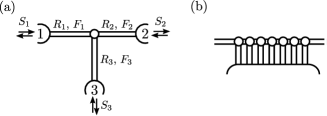
When comparing the semiclassical model to the experiments, we ignore the resistance of the wires under the contacts and use a model of localized contacts. In practice, the large width and low interfacial resistance of the contacts makes the current flow through them non-uniform. Including this fact in the theoretical model by describing the tube using a large number of nodes on top of the contacts (see Fig. 1b) did not improve the fit between the model and the experimental noise data, whereas some improvement was obtained in the fit to the resistance data. This means that a situation between the localized and distributed contacts is realized — however including this fact in the model would increase the number of fitting parameters.
Our individual nanotube samples S1 and S2 were made out of a plasma enhanced CVD MWNTs Koshio with the length of and 5 m and the diameter of nm and 4.0 nm, respectively. The main parameters of the samples are given in Table 1; the noise data is summarized in Tables 2 and 3. The contacts on the PECVD tubes were made using standard e-beam overlay lithography. In these contacts, 2 nm of Ti was employed as an adhesive layer before depositing 30 nm of gold. The width of the four contacts were nm and nm for samples 1 and 2, respectively. The strongly doped Si substrate was employed as the back gate ( aF), separated from the sample by 150 nm of SiO2.
| (nm) | (nm) | (nm) | (nm) | (k) | (k) | (k) | (k) | (k) | (k) | (k) | (k) |
|---|---|---|---|---|---|---|---|---|---|---|---|
| 8.9 | 430 | 300 | 540 | 35 | 30 | 34 | 17.5 | - | 0.5 | 12 | - |
| 27 | 27 | 41 | 17 | 2.4 | 0.1 | 9.7 | |||||
| 4.0 | 940 | 440 | 1110 | 21 | 25 | 28 | 16.5 | - | 5 | 1.7 | - |
| 27 | 16 | 31 | 12 | 2.0 | 1.8 |
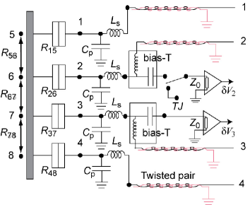
Our measurement setup is illustrated in Fig. 2. Bias-tees are used to separate dc bias and the bias-dependent noise signal at microwave frequencies. We use a LHe-cooled, low-noise amplifier Cryogenics04 with operating frequency range of MHz. A microwave switch and a high-impedance tunnel junction were used to calibrate the gain. Our setup measures voltage fluctuations with respect to ground at the node next to the contact terminal; the voltage fluctuations are converted to current fluctuations by the contact resistance of the measuring terminal. The sample was biased using one voltage source, one lead connected to (virtual) ground of the input of DL1211 current preamplifier and with the remaining two terminals floating.
From four-point measurements at 0.1 - 0.2 V, we get k and k (section 6-7 in Fig. 2) for samples S1 and S2, respectively. Within diffusive transport, this yields for the resistance per unit length km, which amounts to k over the length of a contact. The contact resistances for contacts 2 and 3 of S1 and S2 were determined as averages from a set of two-lead measurements: and ; this scheme was adopted as there is a non-local contribution in voltage Nonlocal . and were found to be nearly constant except for a small region near zero bias. Variation of V changes from to 6 k and from to 3 k on S2 on average. In both cases, increases when going from to (cf. Table 3). We cannot determine the contact resistance of contacts 1 and 4, only the sum of the contact and the nanotube section. For sample 1, we find k, indicating that we have an excellent contact, while k points to a weak, tunneling contact.
The measured noise as a function of current is displayed in Fig. 3 for sample S2. We measured current noise both using DC current, and using AC modulation on top of DC bias: , where represents the noise power integrated over the 250 MHz bandwidth (divided by 50 ) and denotes the differentially measured noise. As seen in Fig. 3, the measured noise for each section of the tube is quite well linear with current at A, while at larger currents the Fano factor decreases gradually with . We determine the Fano factor using linear fits to in the range A: the results vary over 0.1 - 0.5 as seen in Tables 2 and 3.
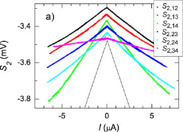
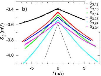
The basic finding of our measurement is that the noise of the sections adjacent to probes 2 and 3 may behave quite differently, depending on how strong the contact is between the gold lead and the nanotube. For terminal 2 of S1, the noise adds in a classical fashion as expected for a good contact, i.e., ( in Table 2). Here, the first index indicates that noise is measured from contact 2 while the bias is applied to the terminal specified by the middle index and the last index tells the grounded contact. For the terminal 3 of S1, on the other hand, we find that . In sample S2, the results are intermediate to the above extreme cases (for example, and ). All the above basic relations are in accordance with semiclassical circuit analysis, while the results related over a good contact can be accounted for by purely classical circuit theory (cf. Eq. (1)).
We fit the semiclassical theory to our data using basically three types of fitting parameters: the tube resistance per unit length , the interfacial resistances in the contact regions, and the Fano factor for the parts of the tube away from contacts. For contacts we use as it makes only a small contribution to noise in good quality contacts. The model thus contains 7 adjustable quantities, and can be used to predict the measured four resistances and the 12 noise correlators. These are fit through a least-square minimization procedure.
Tables 2 and 3 display the calculated results for the noise correlators, while the corresponding resistances are shown in Table I. In both samples the optimum is found with . The classical model, even though consistent with data with good contacts, does not provide a good overall account for either of our samples. The overall agreement of calculated noise with the measurement is %, excluding the two smallest non-local noise values. Within the error bars for the measured data, especially due to the difficulties in determining the exact linear-response resistance values (see below), we obtain an upper limit , i.e. most of the noise comes from the non-equilibrium state generated by the current (as in the last term in Eq. (2)), not from the transport in the tube itself NOTE .
| terminal 2 | terminal 3 | |||||||
|---|---|---|---|---|---|---|---|---|
| Fit | Dev % | Fit | Dev % | |||||
| 0.11 | 0.080 | 0.11 | 15 | 0.006 | 20 | |||
| 0.48 | 0.46 | 0.39 | 16 | 0.41 | 0.39 | 0.38 | 5 | |
| 0.51 | 0.50 | 0.46 | 9 | 0.50 | 0.46 | 0.45 | 7 | |
| 0.41 | 0.40 | 0.29 | 28 | 0.42 | 0.38 | 0.38 | 6 | |
| 0.43 | 0.42 | 0.35 | 17 | 0.54 | 0.47 | 0.45 | 12 | |
| 0.24 | 0.24 | 0.30 | 26 | 0.46 | 0.50 | 0.40 | 18 | |
| Fit | Dev % | |||||||
|---|---|---|---|---|---|---|---|---|
| (k) | 5.8 | 6.4 | 5.3 | 4.9 | 1.8 | 65 | 3.9 | 5.1 |
| 0.26 | 0.24 | 0.21 | 0.20 | 0.19 | 10 | 0.24 | 0.23 | |
| 0.37 | 0.34 | 0.33 | 0.32 | 0.35 | 6 | 0.38 | 0.35 | |
| 0.42 | 0.38 | 0.37 | 0.36 | 0.41 | 11 | 0.36 | 0.36 | |
| 0.25 | 0.23 | 0.24 | 0.25 | 0.23 | 5 | 0.25 | 0.24 | |
| 0.36 | 0.32 | 0.27 | 0.28 | 0.29 | 7 | 0.28 | 0.21 | |
| 0.075 | 0.11 | 0.061 | 0.082 | 0.12 | 64 | 0.055 | 0.053 | |
| Fit | Dev % | |||||||
|---|---|---|---|---|---|---|---|---|
| (k) | 2.4 | 3.3 | 1.4 | 2.1 | 1.7 | 5 | 0.9 | 2.9 |
| 0.081 | 0.079 | 0.13 | 0.13 | 0.13 | 2 | 0.043 | 0.052 | |
| 0.14 | 0.15 | 0.29 | 0.27 | 0.29 | 4 | 0.14 | 0.14 | |
| 0.34 | 0.24 | 0.31 | 0.30 | 0.40 | 30 | 0.20 | 0.21 | |
| - | - | 0.24 | 0.25 | 0.23 | 8 | - | - | |
| 0.26 | 0.19 | 0.40 | 0.35 | 0.33 | 12 | 0.17 | 0.18 | |
| 0.12 | 0.087 | 0.24 | 0.19 | 0.17 | 23 | 0.085 | 0.077 | |
We get from Table 3 average Fano factors and at V for terminals 2 and 3, respectively. These values correspond to ensemble averaged values which describe the combined properties of the tube and its contacts. On the other hand, if we take only the noise from single sections 12 and 23 (or 23 and 34), then the average (0.16), pretty close to the above values. Altogether, the variation of local, single section measurements is 0.10-0.48, quite distinct from simple diffusive wire expectations, and the semiclassical analysis is able to account for all these under the premise that the tube is noise-free! This conclusion is in line with results in SWNT bundles that have shown small noise as well Roche02 . In semiconducting MWNTs rather large noise at 1 GHz has been observed, which has been assigned to the presence of Schottky barriers WuSemi .
The fitted resistances are slightly off from the measured values. This must be partly because in nanotubes it is difficult to avoid uncertainties in four-probe measurements (current goes in part through the voltage probes), and partly because the presence of non-local voltages. In addition, the quality of our MWNTs may be so good that the conduction becomes semiballistic and our analysis is not valid any more. For example, in section 1-2 of S1, the IV curve displays a power law which clearly differs from the rest of the sample. The fitted contact resistances range over k, which is in agreement with typical measured values Schonenberger ; deHeer .
In summary, we have investigated experimentally shot noise of multiterminal MWNTs under several biasing conditions. The noise was found to depend strongly on the contact resistance. At small interfacial resistance, our 0.4-0.5 micron contacts acted as inelastic probes and classical noise analysis was found sufficient. Weaker contacts could be accounted for by using semiclassical theory. The latter allows to comprehend the observed, broad spectrum of Fano-factors, but it leads to the conclusion that the intrinsic noise of MWNTs is nearly zero, at most . Most of the observed noise is generated by metal-nanotube contacts, which govern the non-equilibrium distributions of charge carriers on the tube.
We thank L. Lechner, B. Placais, and E. Sonin for fruitful discussions and S. Iijima, A. Koshio, and M. Yudasaka for the carbon nanotube material employed in our work. This work was supported by the Academy of Finland and by the EU contract FP6-IST-021285-2.
References
- (1) C. Schönenberger, A. Bachtold, C. Strunk, J.-P. Salvetat and L. Forro, Appl. Phys. A 69, 283 (1999).
- (2) See, e.g., B. Stojetz, C. Miko, L. Forró, and C. Strunk Phys. Rev. Lett. 94, 186802 (2005).
- (3) See, F. Wu, et al. cond-mat/0702332, and references therein.
- (4) K.E. Nagaev, Phys. Lett. A 169, 103 (1992); P. Virtanen and T. T. Heikkilä, New J. Phys. 8, 50 (2006).
- (5) Y. Nazarov and D. Bagrets, Phys. Rev. Lett. 88 (2002).
- (6) Ya.M. Blanter, M. Büttiker, Phys. Rep. 336, 1 (2000).
- (7) S. Oberholzer, E. V. Sukhorukov, C. Strunk, and C. Schönenberger, Phys. Rev. B 66, 233304 (2002).
- (8) A. Koshio, M. Yudasaka, and S. Iijima, Chem. Phys. Lett. 356, 595 (2002).
- (9) L. Roschier and P. Hakonen, Cryogenics 44, 783 (2004).
- (10) We recorded the non-local voltage produced by current where ij and kl were 12 (34) and 34 (12), respectively. We obtained for k and k on S1. This is a bit stronger coupling than found in B. Bourlon, et al. Phys. Rev. Lett. 93, 176806 (2004).
- (11) This upper limit was obtained with the localized contact model and assuming for the contacts.
- (12) P. E. Roche, et al., Eur. Phys. J. B 28, 217 (2002).
- (13) F. Wu, et al. Phys. Rev. B 75, 125419 (2007).
- (14) P. Poncharal, C. Berger, Yan Yi, Z. L. Wang, and W. A. de Heer, J. Phys. Chem. B 106, 12104 (2002).