Spin qubits in antidot lattices
Abstract
We suggest and study designed defects in an otherwise periodic potential modulation of a two-dimensional electron gas as an alternative approach to electron spin based quantum information processing in the solid-state using conventional gate-defined quantum dots. We calculate the band structure and density of states for a periodic potential modulation, referred to as an antidot lattice, and find that localized states appear, when designed defects are introduced in the lattice. Such defect states may form the building blocks for quantum computing in a large antidot lattice, allowing for coherent electron transport between distant defect states in the lattice and tunnel coupling of neighboring defect states with corresponding electrostatically controllable exchange coupling between different electron spins.
pacs:
73.21.Cd, 75.30.Et, 73.22.-fI Introduction
Localized electrons spins in a solid state structure have been suggested as a possible implementation of a future device for large-scale quantum information processing.Loss and DiVincenzo (1998) Together with single spin rotations, the exchange coupling between spins in tunnel coupled electronic levels would provide a universal set of quantum gate operations.Burkard et al. (1999) Recently, both of these operations have been realized in experiments on electron spins in double quantum dots, demonstrating electron spin resonance (ESR) driven single spin rotationsKoppens et al. (2006) and electrostatic control of the exchange coupling between two electron spins.Petta et al. (2005) Combined with the long coherence time of the electron spin due to its weak coupling to the environment, and the experimental ability to initialize a spin and reading it out,Elzerman et al. (2004) four of DiVincenzo’s five criteriaDiVincenzo (2000) for implementing a quantum computer may essentially be considered fulfilled. This leaves only the question of scalability experimentally unaddressed.
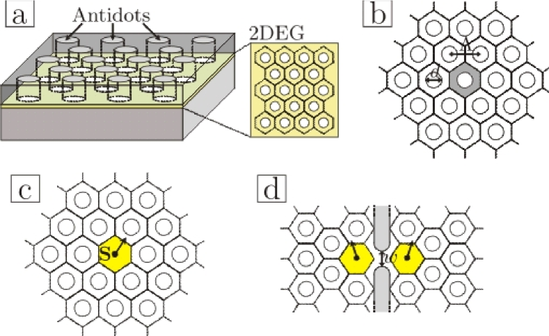
While large-scale quantum information processing with conventional gate-defined quantum dots is a topic of ongoing theoretical research,Taylor et al. (2005) we here suggest and study an alternative approach based on so-called defect states that form at designed defects in a periodic potential modulation of a two-dimensional electron gas (2DEG) residing at the interface of a semiconductor heterostructure.Flindt et al. (2005) One way of implementing the potential modulation would be similar to the periodic antidot latticesEnsslin and Petroff (1990); Weiss et al. (1993) that are now routinely fabricated. Such lattices can be fabricated on top of a semiconductor heterostructure using local oxidation techniques that allow for a precise patterning of arrays of insulating islands, with a spacing on the order of 100 nm, in the underlying 2DEG.Dorn et al. (2005) Even though the origin of these depletion spots is not essential for our proposal, we refer to them as antidots, and a missing antidot in the lattice as a defect. Alternative fabrication methods include electron beam and photo lithography. Luo and Misra (2006); Martín et al. (2003) In Ref. Dorn et al., 2005 a square lattice consisting of antidots was patterned on an approximately 2.5 m 2.5 m area, and the available fabrication methods suggest that even larger antidot lattices with more than 1000 antidots and many defect states may be within experimental reach.
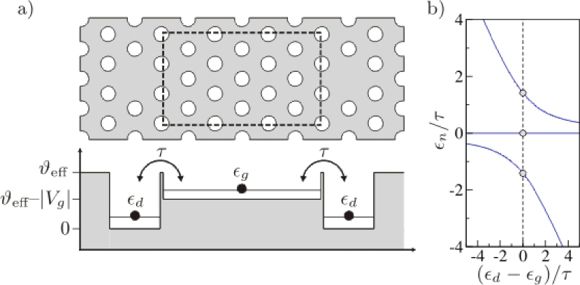
The idea of using designed defects in antidot lattices as a possible quantum computing architecture was originally proposed by some of us in Ref. Flindt et al., 2005, where we presented simple calculations of the single-particle level structure of an antidot lattice with one or two designed defects. Here, we take these ideas further and present detailed band structure and density of states calculations for a periodic lattice, describe a resonant tunneling phenomenon allowing for electron transport between distant defects in the lattice, and calculate numerically the exchange coupling between spins in two neighboring defects, showing that the suggested architecture could be useful for spin-based quantum information processing. The envisioned structure and the basic building blocks are shown schematically in Fig. 1.
The paper is organized as follows: In Section II we introduce our model of the antidot lattice and present numerical results for the band structure and density of states of a periodic antidot lattice. In particular, we show that the periodic potential modulation gives rise to band gaps in the otherwise parabolic free electron band structure. In Section III we introduce a single missing antidot, a defect, in the lattice and calculate numerically the eigenvalue spectrum of the localized defect states that form at the location of the defect. We develop a semi-analytic model that explains the level-structure of the lowest-lying defect states. In Section IV we consider two neighboring defect states and calculate numerically the tunnel coupling between them. In Section V we describe a principle for coherent electron transport between distant defect states in the antidot lattice, and illustrate this phenomenon by wavepacket propagations. In Section VI we present numerically exact results for the exchange coupling between electron spins in tunnel coupled defect states, before we finally in Section VII present our conclusions.
II Periodic antidot lattice
We first consider a triangular lattice of antidots with lattice constant superimposed on a two-dimensional electron gas (2DEG). The structure is shown schematically together with the Wigner-Seitz cell in Fig. 1(b). While experiments on antidot lattices are often performed in a semi-classical regime, where the typical feature sizes and distances, e.g., the lattice constant , are much larger than the electron wavelength, we here consider the opposite regime, where these length scales are comparable, and a full quantum mechanical treatment is necessary. In the effective-mass approximation we thus model the periodic lattice with a two-dimensional single-electron Hamiltonian reading
| (1) |
where is the effective mass of the electron and is the potential of the ’th antidot positioned at . We model each antidot as a circular potential barrier of diameter so that for and zero otherwise. In the limit the eigenfunctions do not penetrate into the antidots, and the Schrödinger equation may be written as
| (2) |
with the boundary condition in the antidots, and where we have introduced the dimensionless eigenvalues
| (3) |
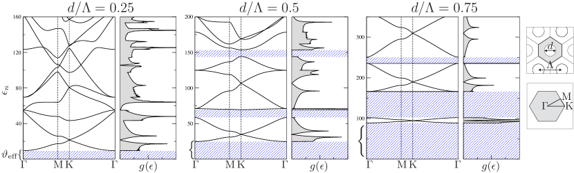
In the following we use parameter values typical of GaAs, for which eV nm2 with , although the choice of material is not essential. We have checked numerically that our results are not critically sensitive to the approximation , so long as the height is significantly larger than any energies under consideration. All results presented in this work have thus been calculated in this limit, for which the simple form of the Schrödinger equation Eq. (2) applies. In this limit, the band structures presented below are of a purely geometrical origin. The band structure can be calculated by imposing periodic boundary conditions and solving Eq. (2) on the finite domain of the Wigner–Seitz cell. We solve this problem using a finite-element method.com The corresponding density of states is calculated using the linear tetrahedron method in its symmetry corrected form.Lehmann and Taut (1972); Hama et al. (1990); Pedersen et al. (2007a)
In Fig. 2 we show the band structure and density of states of the periodic antidot lattice for three different values of the relative antidot diameter . We note that an increasing antidot diameter raises the kinetic energy of the Bloch states due to the increased confinement and that several band gaps open up. We have indicated the gap below which no states exist for the periodic structure. We shall denote as band gaps only those gaps occurring between two bands, and thus we do not refer to the gap below as a band gap in the following. This is motivated by the difference in the underlying mechanisms responsible for the gaps: While the band gaps rely on the periodicity of the antidot lattice, similar to Bragg reflection in the solid state, the gap below represents an averaging of the potential landscape generated by the antidots, and is thus robust against lattice disorder as we have also checked numerically.Pedersen (2007) The lowest band gap is thus present for while the higher-energy band gap only develops for . As the antidot diameter is increased, several flat bands appear with , giving rise to van Hove singularities in the corresponding density of states.
III Defect states
We now introduce a defect in the lattice by leaving out a single antidot. Topologically, this structure resembles a planar 2D photonic crystal, and relying on this analogy we expect one or more localized defect states to form inside the defect.Mortensen (2005) The gap indicated in Fig. 2 may be considered as the height of an effective two-dimensional potential surrounding the defect, and thus gives an upper limit to the existence of defect states in this gap. Similar states are expected to form in the band gaps of the periodic structure, which are highlighted in Fig. 2. As defect states decay to zero far from the location of the defect, we have a large freedom in the way we spatially truncate the problem at large distances. For simplicity we use a super-cell approximation, but with imposed on the edge, thus leaving Eq. (2) a Hermitian eigenvalue problem which we may conveniently solve with a finite-element method.com Other choices, such as periodic boundary conditions, do not influence our numerical results. The size of the super-cell has been chosen sufficiently large, such that the results are unaffected by a further increase in size.
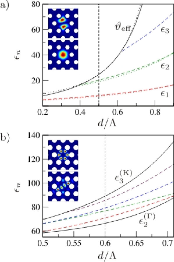
In the insets of Fig. 3(a) we show the calculated eigenfunctions corresponding to the two lowest energy eigenvalues for a relative antidot diameter . As expected, we find that defect states form that to a high degree are localized within the defect. The second-lowest eigenvalue is two-fold degenerate and we only show one of the corresponding eigenstates. The figure shows the energy eigenvalues of the defect states as a function of the relative antidot diameter together with the gap . As this effective potential is increased, additional defect states become available and we may thus tune the number of levels in the defect by adjusting the relative antidot diameter. In particular, we note that for only a single defect state forms. As the sizes of the antidots are increased, the confinement of the defect states becomes stronger, leading to an increase in their energy eigenvalues. For GaAs with and nm the energy splitting of the two lowest defect states is approximately 1.1 meV, which is much larger than at subkelvin temperatures, and the level structure is thus robust against thermal dephasing.
In Fig. 3(b) we show similar results for defect states residing in the lowest band gap of the periodic structure. While the states residing below resemble those occurring due to the confining potential in conventional gate-defined quantum dots, these higher-lying states are of a very different nature, being dependent on the periodicity of the surrounding lattice. For the band gaps, the existence of bound states is limited by the relevant band edges as indicated in the figure. As the size of the band gap is increased, additional defect states become available and we may thus also tune the number of levels residing in the band gaps by adjusting the relative antidot diameter.
Because the formation of localized states residing below depends only on the existence of the effective potential surrounding the defect, the formation of such states is not critically dependent on perfect periodicity of the surrounding lattice, which we have checked numerically.Pedersen (2007) Also, the lifetimes of the states due to the finite size of the antidot lattice are of the order of seconds even for a relatively small number of rings of antidots surrounding the defect.Flindt et al. (2005) However, the localized states residing in the band gaps are more sensitive to lattice disorder, since they rely more crucially on the periodicity of the surrounding lattice. Introducing disorder may induce a finite density of states in the band gaps of the periodic structure and thus significantly decrease the lifetimes of the localized states residing in this region.
In order to gain a better understanding of the level-structure of the defect states confined by we develop a semi-analytic model for and the corresponding defect states. We first note that the effective potential is given by the energy of the lowest Bloch state at the point of the periodic lattice. At this point and Bloch’s theorem reduces to an ordinary Neumann boundary condition on the edge of the Wigner–Seitz cell. This problem may be solved using a conformal mapping, and we obtain the expressionMortensen (2006)
| (4) |
where , and are given by expressions involving the Bessel functions and . Mortensen (2006) We now consider the limit of and note that in this case the defect states residing below are subject to a potential which we may approximate as an infinite two-dimensional spherical potential well with radius . The lowest eigenvalue for this problem is , where is the first zero of the zeroth order Bessel function. This expression yields the correct scaling with , but is only accurate in the limit of . We correct for this by considering the limit of , in which we may solve the problem using ideas developed by Glazman et al. in studies of quantum conductance through narrow constrictions. Glazman et al. (1988) The problem may be approximated as a two-dimensional spherical potential well of height and radius . The lowest eigenvalues of this problem is the first root of the equation
| (5) |
where () is the ’th order Bessel function of the first (second) kind. If the height of the potential well is much larger than the energy eigenvalues, the first root would simply be . Lowering the confinement must obviously shift down the eigenvalue, and in the present case we find that . By expanding the equation to first order in around we may solve the equation to obtain , which is in excellent agreement with a full numerical solution of Eq. (5). Correcting for the low- behavior we thus find the approximate expression for the lowest energy eigenvalueFlindt et al. (2005)
| (6) | |||||
A similar analysis leads to an approximate expression for the first excited state . This mode has a finite angular momentum of and a radial solution yields
| (7) |
where is the second-lowest eigenvalue of the two-dimensional spherical potential well of height and radius , which can be found from an equation very similar to Eq. (5). The first root of the first-order Bessel function is . The scaling of the two lowest eigenvalues with is thus approximately the same. The approximate expressions are indicated by the dotted lines in Fig. 3, and we note an excellent agreement with the numerical results. We remark that the filling of the defect states can be controlled using a metallic back gate that changes the electron density and thus the occupation of the different defect states.foot
IV Tunnel coupled defect states
Two closely situated defect states can have a finite tunnel coupling, leading to the formation of hybridized defect states. The coupling between the two defects may be tuned via a metallic split gate defined on top of the 2DEG in order to control the opening between the two defects. As the voltage is increased the opening is squeezed, leading to a reduced overlap between the defect states. We model such a split gate as an infinite potential barrier shaped as shown in Fig. 1(d). Changing the applied voltage effectively leads to a change in the relative width of the opening, which we take as a control parameter in the following. If we consider just a single level in each defect we can calculate the tunnel matrix element as where are the eigenenergies of the bonding and anti-bonding states, respectively, of the double defect. In the following, we calculate the tunnel coupling between two defect states lying below , but the analysis applies equally well to defect states lying in the band gaps.
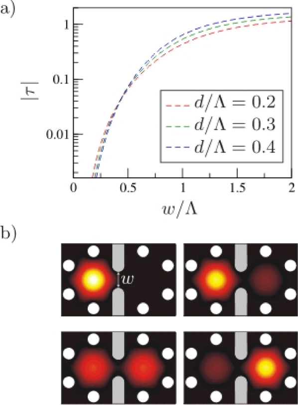
In Fig. 4 we show the tunnel matrix element as a function of the relative gate constriction width for three different values of in the single-level regime of each defect, i.e., . As expected, the tunnel coupling grows with increasing constriction width due to the increased overlap between the defect states. A saturation point is reached when the constriction width is on the order of the diameter of the defect states, after which the overlap is no longer increased significantly. An electron prepared in one of the defect states will oscillate coherently between the two defect states with a period given as , which for GaAs with nm, and implies an oscillation time of ns. A numerical wavepacket propagation of an electron initially prepared in the left defect state is shown in Fig. 4(b), confirming the expected oscillatory behavior. With a finite tunnel coupling between two defect states, two electron spins trapped in the defects will interact due to the exchange coupling, to which we return in Section VI.
V Resonant coupling of distant defect states
With a large antidot lattice and several defect states it may be convenient with quantum channels along which coherent electron transport can take place, connecting distant defect states. In Refs. Nikolopoulos et al., 2004a and Nikolopoulos et al., 2004b it was suggested to use arrays of tunnel coupled quantum dots as a means to obtain high-fidelity electron transfer between two distant quantum dots. We have applied this idea to an array of tunnel coupled defect states and confirmed that this mechanism may be used for coherent electron transport between distant defects in an antidot lattice.Pedersen (2007) This approach, however, relies on precise tunings of the tunnel couplings between each defect in the array, which may be difficult to implement experimentally. Instead, we suggest an alternative approach based on a resonant coupling phenomenon inspired by similar ideas used to couple light between different fiber cores in a photonic crystal fiber.Skorobogatiy et al. (2006a, b)
We consider two defects separated by a central line of antidots and a central back gate in the region between the defects, as shown in Fig. 5. Again, we consider defect states residing below , but the principle described here may equally well be applied to defect states in the band gaps. Using the back gate, the potential between the two defects can be controlled locally. If the potential is lowered below , a discrete spectrum of standing-wave solutions forms between the two defects. In the following we denote the energy of one of these standing-wave solutions by , while the energy of the two defect states is assumed to be identical and is denoted . A simple three-level analysis of this system, as illustrated in Fig. 5, reveals that by tuning the back gate so that the levels are aligned, , a resonant coupling between the two distant defects occurs, characterized by a symmetric splitting of the three lowest eigenvalues into and , where is the tunnel coupling between the defects and the standing-wave solution in the central back gate region. If an electron is prepared in one of the defects states, it will oscillate coherently between the two defects with an oscillation period of . By turning off the back gate at time we may thereby trap the electron in the opposite defect which may by situated a distance an order of magnitude larger than the lattice constant away from the other defect.
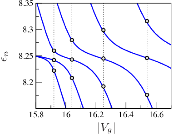
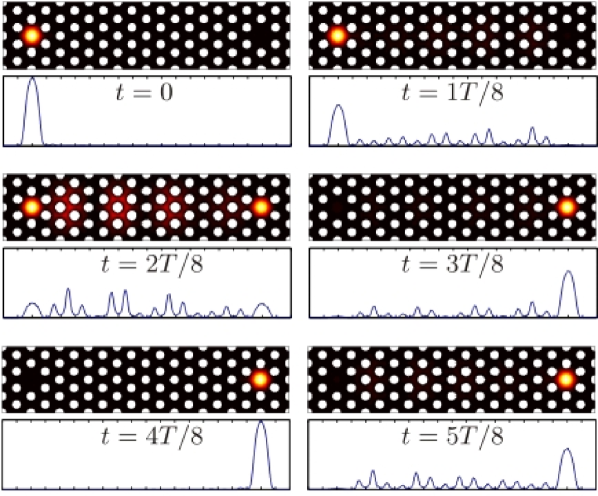
In Fig. 6 we show the numerically calculated eigenvalues as a function of the depth of the central potential square well of the structure illustrated in Fig. 5 for and a central line of antidots separating the two defects. Contrary to the simple three-level model, several resonances now occur as the back gate is lowered, corresponding to coupling to different standing-wave solutions in the multi-leveled central region. The energy splitting at resonance is larger when the defect states couple to higher-lying central states due to a large overlap between the defect states and the central standing-wave solution. In Fig. 7 we show a numerical time propagation of an electron initially prepared in the left defect, confirming the oscillatory behavior expected from the simple model. For GaAs and nm the results indicate an oscillation period of ns for the time propagation illustrated. The resonant phenomenon relies solely on the level alignment and on the symmetry condition that both defect states have the same energy and magnitude of tunnel coupling to the standing wave solution in the central region. It is in principle independent of the number of antidots separating the two defects, but in practice this range is limited by the coherence length of the sample and the fact that the levels of the central region grow too dense if becomes large.foot We have checked numerically that resonant coupling of defect levels below is robust against lattice disorder.Pedersen (2007)
VI Exchange coupling
So far we have only considered the single-particle electronic level-structure of the antidot lattice. However, as mentioned in the introduction, the exchange coupling between electron spins is a crucial building block for a spin based quantum computing architecture, and in fact suffices to implement a universal set of quantum gates. DiVincenzo et al. (2000) The exchange coupling is a result of the Pauli principle for identical fermions, which couples the symmetries of the orbital and spin degrees of freedom. If the orbital wavefunction of the two electrons is symmetric (i.e. preserves sign under particle-exchange), the spins must be in the antisymmetric singlet state, while an antisymmetric orbital wavefunction means that the spins are in a symmetric triplet state. One may thereby map the splitting between the ground state energy of the symmetric orbital subspace and the ground state energy of the antisymmetric orbital subspace onto an effective Heisenberg spin Hamiltonian , where is the exchange coupling between the two spins, and . The implementation of quantum gates based on the exchange coupling requires that can be varied over several orders of magnitude in order to effectively turn the coupling on and off. In this section we present numerically exact results for the exchange coupling between two electron spins residing in tunnel coupled defects as those illustrated in Fig. 1(d).
The Hamiltonian of two electrons in two tunnel coupled defects may be written as
| (8) |
where
| (9) |
is the Coulomb interaction and the single-electron Hamiltonians are
| (10) |
where is the potential due to the antidots and the coupled defects. As previously, we model the antidots and the split gate as potential barriers of infinite height, and use finite-element methods to solve the single-electron problem defined by Eq. (10). A Zeeman field applied perpendicularly to the electron gas splits the spin states, and we choose a corresponding vector potential reading .
In order to calculate the exchange coupling we employ a recently developed method for numerically exact finite-element calculations of the exchange coupling:Pedersen et al. (2007b) The full two-electron problem is solved by expressing the two-electron Hamiltonian in a basis of product states of single-electron solutions obtained using a finite element method.com The Coulomb matrix elements are evaluated by expanding the single-electron states in a basis of 2D Gaussians,Helle et al. (2005) and the two-particle Hamiltonian matrix resulting from this procedure may then be diagonalized in the subspaces spanned by the symmetric and antisymmetric product states, respectively, to yield the exchange coupling. The details of the numerical method are described elsewhere.Pedersen et al. (2007b); Pedersen (2007) The results presented below have all been obtained with a sufficient size of the 2D Gaussian basis set as well as the number of single-electron eigenstates, such that a further increase does not change the results.foot
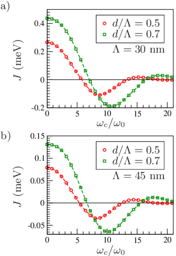
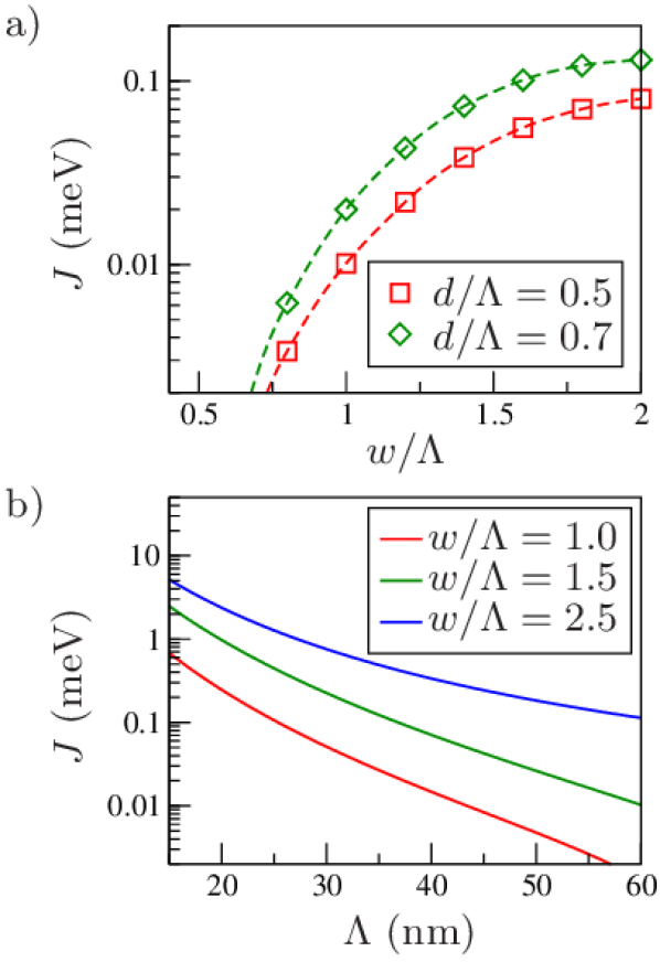
In Fig. 8 we show the calculated exchange coupling for a double defect structure. The exchange coupling varies by several orders of magnitude as the split gate constriction width is increased, showing that electrostatic control of the exchange coupling in an antidot lattice is possible, similarly to the principles proposedBurkard et al. (1999) and experimentally realizedPetta et al. (2005) for double quantum dots. Just as the tunnel coupling, the exchange coupling reaches a saturation point when the split gate constriction width is on the order of the diameter of the defect states. This is to be expected since the exchange coupling in the Hubbard approximation is proportional to the square of the tunnel coupling.Burkard et al. (1999) As illustrated in Fig. 8(b), the exchange coupling is highly dependent on the lattice constant, increasing several orders of magnitude as the lattice constant is decreased from nm to nm. This is in part due to the overall increase in the energies of the eigenstates and the between them with increased confinement, but also due to a decrease in the ratio of the Coulomb interaction strength to the confinement strength. As the relative strength of the Coulomb interaction is decreased, the defect states are effectively moved closer together, resulting in an increase in the exchange coupling.
The exchange coupling is also highly dependent on magnetic fields applied perpendicularly to the plane of the electrons.Burkard et al. (1999) In Fig. 9 we show the exchange coupling as a function of where and we define . For GaAs T-1nm. As expected, the results of Fig. 9 are very similar to those obtained for double quantum dots. Burkard et al. (1999); Helle et al. (2005) In all cases we note an initial transition from the anti-ferromagnetic () to the ferromagnetic () regime of exchange coupling, followed by a return to positive values of the exchange coupling at higher magnetic fields. The initial transition to negative exchange coupling is caused by long-range Coulomb interactions.Burkard et al. (1999) As the magnetic field is increased further, magnetic confinement becomes dominant, compressing the orbits and thus reducing the overlap between the single-defect wave functions. This leads to a strong reduction of the magnitude of the exchange coupling. Due to the increased confinement strength for smaller lattice constants , these transitions occur at larger magnetic fields. The same is the case for the larger relative antidot diameters, in which the ratio of magnetic confinement to confinement due to the antidots is reduced. We have only considered the case of a large constriction width , since this regime of relatively large exchange coupling is the most interesting for practical purposes. For small values of we expect to find results similar to those obtained in the limit of large interdot distances for double quantum dot systems.Burkard et al. (1999)
VII Conclusions
In conclusion, we have suggested and studied an alternative candidate for spin based quantum information processing in the solid-state, namely defect states forming at the location of designed defects in an otherwise periodic potential modulation of a two-dimensional electron gas, here referred to as an antidot lattice. We have performed numerical band structure and density of states calculations of a periodic antidot lattice, and shown how localized defect states form at the location of designed defects. The antidot lattice allows for resonant coupling of distant defect states, enabling coherent transport of electrons between distant defects. Finally, we have shown that electrostatic control of the exchange coupling between electron spins in tunnel coupled defect states is possible, which is an essential ingredient for spin based quantum computing. Altogether, we believe that designed defects in antidot lattices provide several prerequisites for a large quantum information processing device in the solid state.
Acknowledgements.
We thank A. Harju for helpful advice during the development of our numerical routines, and T. G. Pedersen for fruitful discussions during the preparation of this manuscript. APJ is grateful to the FiDiPro program of the Finnish Academy for support during the final stages of this work.References
- Loss and DiVincenzo (1998) D. Loss and D. P. DiVincenzo, Phys. Rev. A 57, 120 (1998).
- Burkard et al. (1999) G. Burkard, D. Loss, and D. P. DiVincenzo, Phys. Rev. B 59, 2070 (1999).
- Koppens et al. (2006) F. H. L. Koppens, C. Buizert, K. J. Tielrooij, I. T. Vink, K. C. Nowack, T. Meunier, L. P. Kouwenhoven, and L. M. K. Vandersypen, Nature 442, 766 (2006).
- Petta et al. (2005) J. R. Petta, A. C. Johnson, J. M. Taylor, E. A. Laird, A. Yacoby, M. D. Lukin, C. M. Marcus, M. P. Hanson, and A. C. Gossard, Science 309, 2180 (2005).
- Elzerman et al. (2004) J. M. Elzerman, R. Hanson, L. H. W. van Beveren, B. Witkamp, L. M. K. Vandersypen, and L. P. Kouwenhoven, Nature 430, 431 (2004).
- DiVincenzo (2000) D. P. DiVincenzo, Fortschr. Phys. 48, 771 (2000).
- Taylor et al. (2005) J. M. Taylor, H. A. Engel, W. Dur, A. Yacoby, C. M. Marcus, P. Zoller, and M. D. Lukin, Nat. Phys. 1, 177 (2005).
- Flindt et al. (2005) C. Flindt, N. A. Mortensen, and A. P. Jauho, Nano Lett. 5, 2515 (2005).
- Ensslin and Petroff (1990) K. Ensslin and P. M. Petroff, Phys. Rev. B 41, 12307 (1990).
- Weiss et al. (1993) D. Weiss, K. Richter, A. Menschig, R. Bergmann, H. Schweizer, K. von Klitzing, and G. Weimann, Phys. Rev. Lett. 70, 4118 (1993).
- Dorn et al. (2005) A. Dorn, E. Bieri, T. Ihn, K. Ensslin, D. D. Driscoll, and A. C. Gossard, Phys. Rev. B 71, 035343 (2005).
- Luo and Misra (2006) Y. Luo and V. Misra, Nanotechnology 17, 4909 (2006).
- Martín et al. (2003) J. I. Martín, J. Nogués, K. Liu, J. L. Vicent, I. K. Schuller, J. Magn. Magn. Mater. 256, 449 (2003).
- (14) We have used the COMSOL Multiphysics 3.2 package for all finite-element calculations. See www.comsol.com. Convergence with respect to the mesh size has been ensured.
- Lehmann and Taut (1972) G. Lehmann and M. Taut, Phys. Status Solidi B 54, 469 (1972).
- Hama et al. (1990) J. Hama, M. Watanabe, and T. Kato, J. Phys. Cond. Matt. 2, 7445 (1990).
- Pedersen et al. (2007a) J. Pedersen, C. Flindt, N. A. Mortensen, and A.-P. Jauho, AIP Conf. Proc. 893, 821 (2007a).
- Pedersen (2007) J. Pedersen, Master’s thesis, Technical University of Denmark (2007).
- Mortensen (2005) N. A. Mortensen, Opt. Lett. 30, 1455 (2005).
- Mortensen (2006) N. A. Mortensen, J. Eur. Opt. Soc., Rapid Publ. 1, 06009 (2006).
- Glazman et al. (1988) L. I. Glazman, G. K. Lesovik, D. E. Khmelnitskii, and R. I. Shekter, JEPT Lett. 48, 238 (1988).
- (22) In practice, reliable single-electron filling may pose a serious experimental challenge which could require further optimization of the architecture presented here.
- Nikolopoulos et al. (2004a) G. M. Nikolopoulos, D. Petrosyan, and P. Lambropoulos, J. Phys. Cond. Matt. 16, 4991 (2004a).
- Nikolopoulos et al. (2004b) G. M. Nikolopoulos, D. Petrosyan, and P. Lambropoulos, Europhys. Lett. 65, 297 (2004b).
- Skorobogatiy et al. (2006a) M. Skorobogatiy, K. Saitoh, and M. Koshiba, Opt. Lett. 31, 314 (2006a).
- Skorobogatiy et al. (2006b) M. Skorobogatiy, K. Saitoh, and M. Koshiba, Opt. Express 14, 1439 (2006b).
- (27) Another experimental challenge relates to the switching time of the back gate which grows with length, making it harder to control on short time scales.
- DiVincenzo et al. (2000) D. P. DiVincenzo, D. Bacon, J. Kempe, G. Burkard, and K. B. Whaley, Nature 408, 339 (2000).
- Pedersen et al. (2007b) J. Pedersen, C. Flindt, N. A. Mortensen, and A.-P. Jauho, Phys. Rev. B 76, 125323 (2007b), arXiv:0706.1859v1.
- Helle et al. (2005) M. Helle, A. Harju, and R. M. Nieminen, Phys. Rev. B 72, 205329 (2005).
- (31) Because we use an expansion in localized single-particle product states our method is most reliable for systems with several localized single-particle states. We consequently focus on relative antidot diameters above the single-level regime of the single defects (), see Fig. 3.