Doping graphene with metal contacts
Abstract
Making devices with graphene necessarily involves making contacts with metals. We use density functional theory to study how graphene is doped by adsorption on metal substrates and find that weak bonding on Al, Ag, Cu, Au and Pt, while preserving its unique electronic structure, can still shift the Fermi level with respect to the conical point by eV. At equilibrium separations, the crossover from -type to -type doping occurs for a metal work function of eV, a value much larger than the graphene work function of 4.5 eV. The numerical results for the Fermi level shift in graphene are described very well by a simple analytical model which characterizes the metal solely in terms of its work function, greatly extending their applicability.
pacs:
73.63.-b, 73.20.Hb, 73.40.Ns, 81.05.UwRecent progress in depositing a single graphene sheet on an insulating substrate by micromechanical cleavage enables electron transport experiments on this two-dimensional system Novoselov:sc04 ; Novoselov:nat05 . Such experiments demonstrate an exceptionally high electron mobility in graphene, quantization of the conductivity, and a zero-energy anomaly in the quantum Hall effect, in agreement with theoretical predictions Shon:jpsj98 ; Ando:jpsj02 ; Gusynin:prl05 ; Katsnelson:natp06 ; Brink:natn07 . The spectacular effects arise from graphene’s unique electronic structure. Although it has a zero band gap and a vanishing density of states at the Fermi energy, graphene exhibits metallic behavior due to topological singularities at the -points in the Brillouin zone Shon:jpsj98 ; Ando:jpsj02 where the conduction and valence bands touch in conical (Dirac) points and the dispersion is essentially linear within eV of the Fermi energy.
In a free-standing graphene layer the Fermi energy coincides with the conical points but adsorption on metallic (or insulating) substrates can alter its electronic properties significantly Oshima:jpcm97 ; Dedkov:prb01 ; Bertoni:prb05 ; NDiaye:prl06 ; Karpan:prl07 ; Giovannetti:prb07 ; Marchini:prb07 ; Uchoa:prb08 . Since electronic transport measurements through a graphene sheet require contacts to metal electrodes Novoselov:nat05 ; Karpan:prl07 ; Schomerus:prb07 ; Blanter:prb07 it is essential to have a full understanding of the physics of metal-graphene interfaces. In this paper we use first-principles calculations at the level of density functional theory (DFT) to study the adsorption of graphene on a series of metal substrates. The (111) surfaces of Al, Co, Ni, Cu, Pd, Ag, Pt and Au, covering a wide range of work functions and chemical bonding, form a suitable system for a systematic study.
Our results show that these substrates can be divided into two classes. The characteristic electronic structure of graphene is significantly altered by chemisorption on Co, Ni and Pd but is preserved by weak adsorption on Al, Cu, Ag, Au and Pt. Even when the bonding is weak, however, the metal substrates cause the Fermi level to move away from the conical points in graphene, resulting in doping with either electrons or holes. The sign and amount of doping can be deduced from the difference of the metal and graphene work functions only when they are so far apart that there is no wave function overlap. At the equilibrium separation, the doping level is strongly affected by an interface potential step arising from the direct metal-graphene interaction.
Based upon the DFT results, we develop a phenomenological model to describe the doping of graphene, taking into account the metal-graphene interaction. The model uses only the work functions of graphene and of the clean metal surfaces as input. For a given metal substrate, it allows us to predict the Fermi level shift in graphene with respect to the conical points i.e., both the type and concentration of the charge carriers. The model also predicts how metal work functions are modified by adsorption of graphene.
| Gr | Ni | Co | Pd | Al | Ag | Cu | Au | Pt | |
|---|---|---|---|---|---|---|---|---|---|
| (Å) | 2.05 | 2.05 | 2.30 | 3.41 | 3.33 | 3.26 | 3.31 | 3.30 | |
| (meV) | 125 | 160 | 84 | 27 | 43 | 33 | 30 | 38 | |
| (eV) | 5.47 | 5.44 | 5.67 | 4.22 | 4.92 | 5.22 | 5.54 | 6.13 | |
| (eV) | 4.48 | 3.66 | 3.78 | 4.03 | 4.04 | 4.24 | 4.40 | 4.74 | 4.87 |
| (eV) | 3.9111Ref. Oshima:jpcm97 |
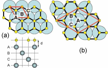
Some details of how DFT ground state energies and optimized geometries are calculated for graphene on metal (111) surfaces are given in Ref. compdetails . We fix the in-plane lattice constant of graphene to its optimized value Å and adapt the lattice constants of the metals accordingly. The graphene honeycomb lattice then matches the triangular lattice of the metal (111) surfaces in the unit cells shown in Fig. 1. The approximation made by this procedure is reasonable, since the mismatch with the optimized metal lattice parameters is only 0.8-3.8%. We have verified explicitly that the structures shown in Fig. 1 represent the most stable configurations of graphene on the metal substrates studied. The equilibrium separations, binding energies and work functions are listed in Table 1.
The results immediately show that the metals can be divided into two classes. Graphene is chemisorbed on Co, Ni and Pd(111), leading to binding energies eV/carbon atom and equilibrium separations Å. In contrast, adsorption on Al, Cu, Ag, Au and Pt(111) leads to a weaker bonding, eV/carbon atom, and larger equilibrium separations, Å. These results are in agreement with previous calculations and experimental data Oshima:jpcm97 ; Bertoni:prb05 ; Karpan:prl07 ; Gamo:ss97 ; Qi:ss05 .
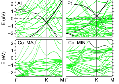
To identify the changes in the graphene electronic structure induced by adsorption, we calculate the band structures as illustrated in Fig. 2 for some typical examples. When graphene is chemisorbed (on Co, Ni, and Pd) the graphene bands are strongly perturbed and acquire a mixed graphene-metal character. In particular, the characteristic conical points at are destroyed, see the bottom panels of Fig. 2. When the interaction is weaker (Al, Cu, Ag, Au, Pt), the graphene bands, including their conical points at , can still be clearly identified; see the upper panels of Fig. 2. However, whereas in free-standing graphene the Fermi level coincides with the conical point, adsorption generally shifts the Fermi level. A shift upwards (downwards) means that electrons (holes) are donated by the metal substrate to graphene which becomes -type (-type) doped.
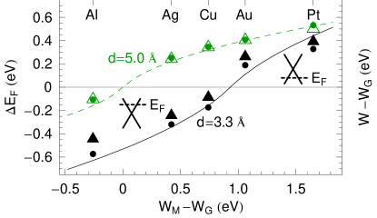
For metal-graphene equilibrium separations, graphene is doped -type on Al, Ag and Cu, and -type on Au and Pt; the corresponding Fermi level shifts are plotted in Fig. 3. Because the work functions of graphene, , and of most metal surfaces, , differ, as soon as graphene interacts with a metal, electrons are transferred from one to the other to equilibrate the Fermi levels. A schematic representation is shown in Fig. 4 for the case of electron transfer from graphene to the metal. To a good approximation, the graphene density of states (DOS) is described by , with /( unit cell) for within 1 eV of the conical points. Since this DOS is much lower than that of the metal, equilibrium is effectively achieved by moving the Fermi level in graphene and even a small electron transfer will shift the Fermi level significantly. A transfer of 0.01 electrons would lower the Fermi level by 0.47 eV.
This electron transfer results in the formation of an interface dipole layer and an accompanying potential step . We can use the plane-averaged electron densities to visualize the electron redistribution upon formation of the interface. As shown in Fig. 4, is localized at the interface. The sign and size of the interface dipole are consistent with the changes of the metal work function upon adsorption of graphene, see Table 1.
Naively one would assume that graphene is doped with electrons if and doped with holes if . The crossover point from - to -type doping would then be at . The results obtained at the equilibrium separations of the graphene sheet and the metal surfaces ( Å; see Fig. 3) show that this is clearly not the case. Instead, the crossover point lies at eV. Only when the graphene-metal separation is increased significantly does the crossover point decrease to its expected value, as illustrated by the upper curve for Å in Fig. 3. This clearly demonstrates that the charge redistribution at the graphene-metal interface is not only the result of an electron transfer between the metal and the graphene levels. There is also a contribution from a metal-graphene chemical interaction. Such an interaction, which has a significant repulsive contribution, has been found to play an important role in describing dipole formation when closed shell atoms and molecules are adsorbed on metal surfaces Silva:prl03 ; Rusu:thesis07 .
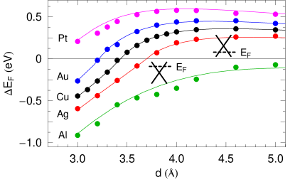
The dependence of this interaction on the metal-graphene separation is mapped out in Fig. 5 in terms of the dependence of the Fermi level shift on . We use the parameters shown in Fig. 4 to construct a simple and general model with which to understand these results. The work function of the graphene-covered metal is given by where is the potential change generated by the metal-graphene interaction. The Fermi level shift in graphene is modeled as . The key element is modeling the potential step in terms of a “non-interacting” charge transfer contribution driven by the difference in work functions and a contribution resulting from the metal-graphene chemical interaction.
The charge transfer contribution is modeled by a plane capacitor model as indicated in Fig. 4. where eV/Å with Å2 the area of the graphene unit cell and is the number of electrons (per unit cell) transferred from graphene to the metal (becoming negative if electrons are transferred from the metal to graphene). is the effective distance between the charge sheets on graphene and the metal. as most of the charge is located between the graphene layer and the metal surface as illustrated in Fig. 4. We model it as with a constant.
Integrating the (linear) density of states of graphene yields a simple relation between and : . Using the relations introduced in the previous two paragraphs we can then express as
| (1) |
where the sign of is given by the sign of . The parameters and turn out to depend only very weakly on the metal substrate. If we fit these quantities to the DFT results for one metal substrate, we can use them as universal parameters to predict the Fermi level shifts in graphene for all metal substrates. We use the DFT results obtained for graphene on Cu (111) to fix and , see Ref. footnote2 . Only the work function of the clean metal surface, , and that of free-standing graphene, , are then needed to calculate the Fermi level shift. The accuracy of the model represented by Eq. (1) is demonstrated in Figs. 3 and 5. From one can immediately obtain the work function of the metal-graphene system, as well as the sign and concentration of the charge carriers in graphene, .
The critical metal work function where the Fermi level is at the conical points of graphene, can be obtained from Eq. (1) for . It gives . The contribution of the chemical interaction term depends strongly on the distance between graphene and the metal surface. At a large distance Å, eV and eV, whereas at the equilibrium separation Å, eV and eV. This agrees with the DFT results shown in Fig. 3. The chemical interaction thus leads to a sizeable potential step at the equilibrium separation, which is downwards from metal to graphene as indicated in Fig. 4. The sign of this step and its insensitivity to the metal substrate are consistent with its interpretation in terms of an exchange repulsion between the electrons on graphene and the metal substrate Rusu:thesis07 .
In conclusion, we have used DFT calculations to study the doping of graphene induced by adsorption on metal surfaces and developed a simple model that takes into account the electron transfer between the metal and graphene levels driven by the work function difference, as well as the chemical interaction between graphene and the metal. The model extends the applicability of the detailed DFT results to the more complex systems encountered in practical devices and suggests combinations of metal (strips) to be used to realize - junctions Cheianov:prb06 .
We thank Paul Rusu for helpful discussions. This work was financially supported by “NanoNed” (a programme of the Dutch Ministry of Economic Affairs) and by the “Nederlandse Organisatie voor Wetenschappelijk Onderzoek (NWO)” via “Chemische Wetenschappen (CW)” and “Stichting voor Fundamenteel Onderzoek der Materie (FOM)”. Computer facilities were granted by “Stichting Nationale Computerfaciliteiten (NCF)”.
References
- (1) K. S. Novoselov et al., Science 306, 666 (2004).
- (2) K. S. Novoselov et al., Nature 438, 197 (2005).
- (3) N. H. Shon and T. Ando, J. Phys. Soc. of Japan 67, 2421 (1998).
- (4) T. Ando et al., J. Phys. Soc. of Japan 71, 1318 (2002).
- (5) V. P. Gusynin and S. G. Sharapov, Phys. Rev. Lett. 95, 146801 (2005).
- (6) M. I. Katsnelson et al., Nat. Phys. 2, 620 (2006).
- (7) J. van den Brink, Nat. Nanotech. 2, 199 (2007).
- (8) C. Oshima and A. Nagashima, J. Phys.: Condens. Mater. 9, 1 (1997).
- (9) Yu. S. Dedkov et al., Phys. Rev. B 64, 035405 (2001).
- (10) G. Bertoni et al., Phys. Rev. B 71, 075402 (2005).
- (11) A. T. N’Diaye et al., Phys. Rev. Lett. 97, 215501 (2006).
- (12) V. M. Karpan et al., Phys. Rev. Lett. 99, 176602 (2007).
- (13) G. Giovannetti et al., Phys. Rev. B 76, 073103 (2007).
- (14) S. Marchini et al., Phys. Rev. B 76, 075429 (2007).
- (15) B. Uchoa et al., Phys. Rev. B 77, 035420 (2008).
- (16) H. Schomerus, Phys. Rev. B 76, 045433 (2007).
- (17) Ya. M. Blanter and I. Martin, Phys. Rev. B 76, 155433 (2007).
- (18) We use a plane wave basis set with a kinetic energy cutoff of 400 eV in the PAW formalism, at the level of the local spin density approximation, as implemented in VASP Kresse:prb96 . The supercell contains a slab of six layers of metal atoms with a graphene sheet adsorbed on one side and a vacuum region of Å. A dipole correction is used Neugebauer:prb92 . We apply and k-point grids to sample the Brillouin Zone (BZ) of the small and large cells in Fig. 1, respectively, and use the tetrahedron method for BZ integrations that include the , and special points. Total energies are converged to eV.
- (19) G. Kresse and J. Furthmuller, Phys. Rev. B 54, 11169 (1996); ibid. Comp. Mat. Sci. 6, 15 (1996).
- (20) J. Neugebauer and M. Scheffler, Phys. Rev. B 46, 16067 (1992).
- (21) Y. Gamo et al., Surf. Science 374, 61 (1997).
- (22) Yue Qi et al., Surf. Science 581, 155 (2005).
- (23) J. L. F. Silva et al., Phys. Rev. Lett. 90, 066104 (2003).
- (24) P. C. Rusu, PhD thesis; http://purl.org/utwente/58034.
- (25) We obtain by least-squares fitting Eq. (1) to the DFT results for for Cu (111) with Å. This value of provides the best fit of for other metal surfaces. At large the chemical interaction term should vanish. Therefore, parametrizing gives Å-1, eV, eV/Å, eV/Å2, where . The general applicability of this equation to all metal substrates can be explained from the weak metal-graphene interaction. The charge redistribution is then dominated by exchange repulsion and is almost independent of the metal species Rusu:thesis07 .
- (26) V. V. Cheianov and V. I. Fal’ko, Phys. Rev. B 74, 041403 (2006); C.-H. Park et al., Nat. Physics 4, 213 (2008).