Nanogaps with very large aspect ratios for electrical measurements
Abstract
For nanoscale electrical characterization and device fabrication it is often desirable to fabricate planar metal electrodes separated by large aspect ratio gaps with interelectrode distances well below 100 nm. We demonstrate a self-aligned process to accomplish this goal using a thin Cr film as a sacrificial etch layer. The resulting gaps can be as small as 10 nm and have aspect ratios exceeding 1000, with excellent interelectrode isolation. Such Ti/Au electrodes are demonstrated on Si substrates and are used to examine a voltage-driven transition in magnetite nanostructures. This shows the utility of this fabrication approach even with relatively reactive substrates.
pacs:
81.07.-b,81.16.-c,85.35.-pThere is much interest in the electronic characterization of nanoscale materials and the creation of working molecular-based devices MolEl_review_2000 . Both goals demand the fabrication of metallic electrodes separated by a distance comparable with the targeted length, i.e. a few nanometers. Much recent progress has been made in nanogap fabrication, and several techniques were proposed, including electromigration EM1_1999 ; EM2_2005 ; EM3_2002 , electrodeposition ED1_2002 ; ED2_2000 , mechanically controlled break junctions BreakJunc_Tour_1997 , advanced e-beam lithography methods Ebeam_align_2000 ; Ebeam_TEM_2007 ; Ebeam_OverExp_2002 ; Ebeam_UnderExp_1990 ; Ebeam_BackSc_2006 , on-wire lithography OnWireLitho_2005 , etc. Interelectrode distances down to 1-2 nm may be achieved EM3_2002 ; ED2_2000 ; Ebeam_TEM_2007 by some of these methods, though without much control of gap aspect ratio.
A significant challenge is fabricating two electrodes separated by a nanometer gap running parallel over a macroscopic width (high-aspect-ratio (HAR) nanogaps). HAR nanogap fabrication has been demonstrated based on a selective etching of cleaved GaAs/AlGaAs heterostructures Tornow_2005 ; HARgap_2007 . However, this method requires particular substrates and allows only restricted gap geometries. A much simpler technique was proposed recently Wind2_2006 with potentially no limitations on the width of the gap. Two separate lithographic patterning steps are used to define first and second electrodes, while the interelectrode separation is controlled by the oxidation of an Al sacrificial layer deposited upon the first electrode. The native aluminum oxide layer, Al2O3, overhangs the underlying metal and serves as a mask during the deposition of the second electrode. This layer must be removed afterwards, but since Al2O3, corundum, is one of the most chemically inert materials EtchReview_2003 , removal by direct chemical etching is very difficult. In a refinement, the authors deposited an additional sacrificial layer of SiO2 and subsequently used etchant for SiO2 to remove the SiO2 and Al/Al2O3 layers Wind2_2006 . The use of SiO2 etchant greatly limits the use of this approach in conjunction with conventional silicon electronics. While this method potentially allows fabrication of HAR nanogaps, the reported aspect ratios are less than 10 Wind2_2006 .
In this letter we report a highly reproducible and flexible method for nanometer-sized (10-20 nm) gap fabrication with aspect ratios exceeding 1000. Modifying the original method Wind2_2006 by replacing the Al layer with Cr results in a significantly more flexible process. A recipe is presented for effectively unlimited aspect ratios with nearly 100% yield. Fabricated nanogap devices were used for nanoscale electrical characterization of magnetite thin films. A characteristic conductance phenomenon related to magnetite thin filmsOur_magnetite_2007 was observed indicating that electronic transport is dominated by the nanometer region between electrodes and there are no cross-gap shorts along gaps tens of m wide. These nanogaps allow studies of this conductance switching at voltages lower than those required in magnetite devices made with standard lithography.
Electrode fabrication consists of three main steps outlined in Fig. 1. Starting substrates were either silicon wafers with 200 nm thermally grown SiO2 layer, or 40-60 nm thick magnetite films on MgO substrates Schvets_JAP_2004 . Poly-(methylmethacrylate) (2% in chlorobenzene) was spin-coated at 3000 rpm on the wafers to form a 500 nm resist layer, followed by baking at 180 ∘C for 2 min. Conventional electron beam lithography (JEOL 6500, 30kV) was used to define the first electrode. After e-beam exposure the pattern was developed in a 1:3 volume mixture of methyl-isobutyl-ketone (MIBK) and isopropanol (IPA) at room temperature (RT). Metallization via electron beam evaporation of 1 nm Ti (adhesion layer), 15 nm Au and 10-45 nm Cr layers followed, with subsequent lift-off in acetone to complete the first electrode (Fig. 1a).

Exposure to ambient conditions results in an oxide layer (CrxOy) (Fig. 1b) that overhangs the edges of the first Ti/Au electrode. A second Ti/Au electrode is then fabricated by e-beam lithography with only rough micrometer alignment of the second electrode relative to the first one. During the deposition of the second electrode 1 nm Ti (0.1 nm/sec) and 15 nm Au (0.2 nm/sec) layers, the CrxOy oxide on top of the first Ti/Au electrode protects an few-nm-wide strip of substrate around the first Ti/Au electrode (Fig. 1c). The suggested “double pad” geometry of the second-step electrode (Fig. 1c) simultaneously produces two addressable gaps in one step. Varying the source-sample distance (30-45 cm) and deposition rates (0.1-0.2 nm/s) had no effect on the results.
Finally the wafer was placed into chromium etchant solution (CR-7, Cyantek) at room temperature for 1.5 min. to remove the Cr/CrxOy layer and overlying second-step Ti and Au layers on top of the first-step electrode. As a result two pairs of electrodes are produced, each pair separated by a nanogap defined by the thickness of CrxOy layer (Fig. 1d). For fixed Cr thickness, the aspect ratio of the gap is set by the width of the second-step electrode and can be varied over a large range; devices with 10-20 nm gaps 10-20 m wide were successfully fabricated. The overall yield of the process (unshorted devices) is limited by the etching yield, and approaches nearly 100% when Cr layer thickness is optimized.
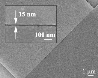
Representative scanning electron micrographs of such electrodes on a Si/SiO2 wafer and Fe3O4 film on MgO substrate are shown on Fig. 2 and Fig. 4 inset, respectively. The gap separation is 10-20 nm for electrodes on Si/SiO2 wafer and 20 nm for the magnetite film. This separation (10-20 nm) is much larger than the expected thickness of native amorphous CrxOy formed at ambient conditions (2 nm Cr_native ). Increasing the thickness of the Cr layer leads to wider gaps (Fig. 3), also inconsistent with the formation of only native oxide.
While the precise mechanism is still under investigation, two factors likely contribute to this dependence on Cr thickness. First, partial thermal oxidation of the Cr layer may increase the oxide thickness, since during the fabrication procedure the chromium layer undergoes two heating processes: an elevated temperature in the evaporator chamber during the evaporation process, and PMMA baking for second step lithography (180 ∘C, 2 min). Thermal oxide growth of CrxOy primarily takes place through outward cation diffusion; thus new oxide forms mainly on top of the existing scaleCr_Mech , increasing the resulting oxide layer overhang and gap size. Second, internal stresses generated within the (primarily) Cr layer due to inward diffusion of oxygenCr_stress may lead to elastic deformation of the underlying Cr. Shear stresses at the Cr/CrxOy interface would produce a deformation of the Cr layer that would favor increased gap size and would increase with Cr layer thickness, as observed in the experiment (Fig. 3). Complete oxidation of the Cr layer is unlikely, since significant oxidation of Cr typically requires temperatures exceeding 300 ∘CGraham_2002 .
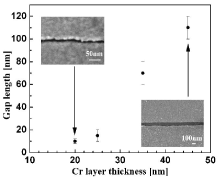
Significantly decreasing the thickness of the Cr layer to achieve narrow gaps increases the threat of accidental connections bridging the gap. An image of the gap produced by means of a 15-20 nm thick sacrificial Cr layer shows that the gap size is well below 10 nm (Fig. 3 inset), but the electrodes are not completely separated from each other with some minor connections being clearly observed in larger images. The gap edge of the second-deposition electrodes tends to be more rough than that of the first-deposition electrodes because of the morphologyCr_native of the CrxOy film.
The thickness of the Cr layer also appears to be critical in the etching process; when the Cr layer thickness is below 10 nm, the wet etching consistently resulted in the overlying second-deposition Ti and Au layer fragments landing on the gap, shorting the two electrodes. Presumably, the etching rate of chromium layer is so rapid that the overlying Ti/Au layer sticks to the first electrode before it can be washed away. Thus, the optimum thickness of the Cr layer is 25 nm to assure the reliable formation of narrowest but at the same unshorted gaps (Figs. 3, 2).
Electrodes produced with this technique on Si/SiO2 wafers were electrically tested for shorting at room temperature (300K). Upon voltage sweeps from 0 V to 0.1 V more than 90% of devices showed currents below the measurable limit (pA), indicating an interelectrode resistance exceeding tens of G. This proves complete isolation of the two electrodes without any connections or gap irregularities narrow enough ( 1-2 nm) to allow tunneling.
We apply this fabrication process to examine the electronic properties of thin (40-60 nm) single-crystal magnetite films grown on MgO substrates Schvets_JAP_2004 . Magnetite undergoes a first-order phase transition when cooled through 122 K, known as the Verwey temperature, , with a structural deformation accompanied by a drastic decrease in electrical conductivity Verwey_1947 . Above TV magnetite behaves as a “bad metal” whereas below TV insulating behavior is observed. In recent nanoscale transport experiments, magnetite nanostructures (both nanocrystals and single-crystal thin films with lithographically defined electrodes) were shown to exhibit a sharp, voltage-driven transition in their electrical conduction at temperatures below Our_magnetite_2007 . At a given temperature the transition voltage is observed to decrease with decreasing interelectrode gap size; thus HAR nanogaps are ideal structures for examining this transition.
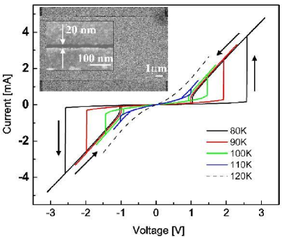
As a representative example, Fig. 4 shows current-voltage characteristics of 50nm-thick film at different temperatures. Sharp conduction transitions hysteretic in voltage below 120 K are evident. Upon approaching a temperature-dependent switch-ON voltage, the conductance (current) jumps 1-2 orders of magnitude, nearly approaching the conductance of the high-temperature “metallic” state of magnetite. The switching voltages increase as temperature decreases while conductance after the transition remains essentially the same. The devices enabled by the HAR fabrication technique allow us to achieve the necessary electric field strengths for switching at relatively modest voltages (below 1V at 110K (Fig. 4), reducing the risk of sample damage and heating. The HAR nanogaps lead to uniform electric fields across the channel.
Fabrication of magnetite devices with the required small gap spacings via the Cr HAR method has been much more reliable and consistent than attempts to do so using two-step e-beam lithography. Furthermore, the survival of the relatively sensitive Fe3O4 film during this process shows the chemical selectivity and versatility of the Cr-based technique. In addition to Ti/Au metallization our technique was successfully applied to fabricate Pt, Al, Fe and Ti electrodes on Si/SiO2 wafers. The HAR closely-spaced electrodes enabled by this approach should find broad applicability in nanoscale electronic measurements.
This work was supported by the US Department of Energy grant DE-FG02-06ER46337. DN also acknowledges the David and Lucille Packard Foundation and the Research Corporation, and Z.K. Keane and C. Slavonic for valuable contributions in the early stages of this work. RGSS and IVS acknowledge the Science Foundation of Ireland grant 06/IN.1/I91.
References
- (1) C. Joachim, J. K. Gimzewski, and A. Aviram, Nature 408, 541 (2000).
- (2) H. Park, A. Lim, A. Alivisatos, J. Park, and P. McEuen, Appl. Phys. Lett. 75, 301 (1999).
- (3) D. Strachan et al., Appl. Phys. Lett. 86, 043109 (2005).
- (4) P. Jiwoong et al., Nature 417, 722 (2002).
- (5) Y. Kervennic, H. Van der Zant, A. Morpurgo, L. Gurevich, and L. Kouwenhoven, Appl. Phys. Lett. 80, 321 (2002).
- (6) C. Z. Li, H. X. He, and N. J. Tao, Appl. Phys. Lett. 77, 3995 (2000).
- (7) M. A. Reed, C. Zhou, C. J. Muller, T. P. Burgin, and J. M. Tour, Science 278, 252 (1997).
- (8) M. Guillorn, D. Carr, R. Tiberio, E. Greenbaum, and M. Simpson, J. Vac. Sci. Technol. B 18, 1177 (2000).
- (9) M. Fischbein and M. Drndić, Nano Lett. 7, 1329 (2007).
- (10) K. Liu et al., Appl. Phys. Lett. 80, 865 (2002).
- (11) B. Van der Gaad and A. Scherer, Appl. Phys. Lett. 56, 481 (1990).
- (12) M. Fischbein and M. Drndić, Appl. Phys. Lett. 88, 063116 (2006).
- (13) L. Qin, S. Park, L. Huang, and C. Mirkin, Science 309, 113 (2005).
- (14) S. Luber et al., Nanotechnology 16, 1182 (2005).
- (15) S. Luber et al., Small 3, 285 (2007).
- (16) J. Tang, Y. Wang, C. Nuckolls, and S. J. Wind, J. Vac. Sci. Tech. B 24, 3227 (2006).
- (17) K. Williams, K. Gupta, and M. Wasilik, J. Microelectromech. Syst. 12, 761 (2003).
- (18) S. Lee et al., Nature Mater. 7, 130 (2008).
- (19) Y. Zhou, X. Jin, and I. V. Shvets, J. Appl. Phys 95, 7357 (2004).
- (20) D. J. Young and M. Cohen, J. Electrochem. Soc. 124, 769 (1977).
- (21) R. Hussey, D. Mitchell, and M. Graham, Werkstoffe und Korrosion 38, 575 (1987).
- (22) D. Caplan and G. I. Sproule, Oxid. Met. 9, 459 (1975).
- (23) M. J. Graham and R. J. Hussey, Corros. Sci. 44, 319 (2002).
- (24) E. J. Verwey, P. W. Haayman, and F. C. Romeijn, J. Chem. Phys. 15, 181 (1947).