Theory of huge tunneling magnetoresistance in graphene
Abstract
We investigate theoretically the spin-independent tunneling magnetoresistance effect in a graphene monolayer modulated by two parallel ferromagnets deposited on a dielectric layer. For the parallel magnetization configuration, Klein tunneling can be observed in the transmission spectrum, but at specific oblique incident angles. For the antiparallel magnetization configuration, the transmission can be blocked by the magnetic-electric barrier provided by the ferromagnets. Such a transmission discrepancy results in a tremendous magnetoresistance ratio and can be tuned by the inclusion of an electric barrier.
pacs:
73.23.-b, 03.65.Pm, 73.43.Cd, 75.70.AkRecent experiments have demonstrated the stability of graphene (a single atomic layer of graphite) and the feasibility of controlling its electrical properties by local gate voltages,Graphene fabrication1 ; Graphene fabrication2 ; Graphene fabrication3 ; half QHE ; gate control1 ; gate control2 opening a promising way to explore carbon-based nanoelectronics. In graphene, the energy spectrum of carriers consists of two valleys labeled by two inequivalent points (referred to as and ) at the edges of the hexagonal Brillouin zone. In each valley, the energy dispersion relation is approximately linear near the points where the electron and hole bands touch. Such a peculiar band structure results in many interesting phenomena, including the half-integer quantum Hall effectGraphene fabrication2 ; Graphene fabrication3 ; half QHE and minimum conductivity.Graphene fabrication2 ; Graphene fabrication3 Further, Dirac-like fermions in graphene can transmit through high and wide electrostatic barriers almost perfectly, in particular for normal incidence.Klein tunneling1 ; Klein tunneling2 ; Klein tunneling3 Such a phenomenon, known as Klein tunneling, leads to a poor rectification effect in graphene p-n junctionsgate control2 and thus may limit the performance of graphene-based electronic devices.
Very recently, inhomogeneous magnetic fields on the nanometer scale have been suggested to confine massless two-dimensional (2D) Dirac electrons,magnetic confinement providing another clue to the manipulation of electrons in graphene. For conventional semiconductor two-dimensional electron gas systems, the patterned local magnetic fields define various magnetic nanostructures ranging from magnetic barriers and wellsmagnetic barrier1 to magnetic dots and antidots.magnetic barrier2 A great deal of experimental and theoretical works have been devoted to understand physical properties of Schrödinger fermions in these systems. The effects of nonuniform magnetic field modulations on 2D Dirac-Weyl fermions, however, has not been investigated as thoroughly, especially for the Klein tunneling under inhomogeneous magnetic field. In this work we explore ballistic transport features of graphene under the modulations of both local magnetic fields and local electrostatic barriers generated by two parallel ferromagnetic stripes. A remarkable tunneling magnetoresistance (TMR) effect is predicted and its physical mechanism is explained.
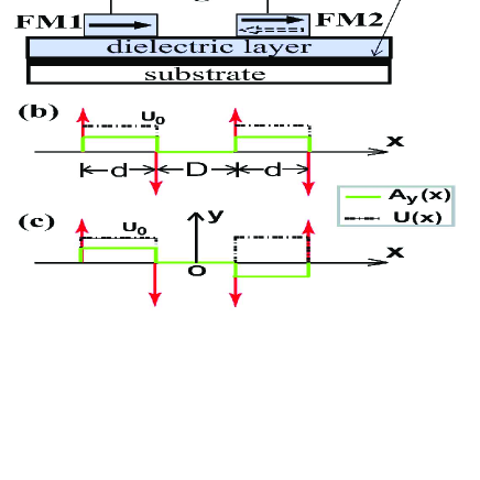
The system under consideration is a single-layer graphene sheet covered by a thin dielectric layer,gate control1 ; gate control2 as sketched in Fig. 1(a). Two parallel ferromagnetic metal (FM) stripes are deposited on top of the insulating layer to influence locally the motion of Dirac electrons in the graphene () plane. Both FM stripes have a width and a magnetization in parallel or in antiparallel to the current direction (the axis). Their fringe fields thus provide a perpendicular magnetic modulation , which is assumed to be homogeneous in the direction and only varies along the axis. A suitable external in-plane magnetic field can change the relative orientation of the two magnetizations which are antiparallel at zero field. At the limit of a small distance between the graphene plane and the ferromagnets, the magnetic barrier can be approximated by several delta functions, i.e., . Here, gives the strength of the local magnetic field, is the magnetic length for an estimated magnetic field , represents the magnetization configuration [ or parallel (P)/antiparallel (AP)], is the distance between the two FM stripes, and is the total length of the structure along the transport direction. The model magnetic field configurations for are depicted in Figs. 1(b) and 1(c), respectively. Further, when a negative gate voltage is applied to both FM stripes, a tunable electrostatic double barrier potential arises in the graphene layer. A square shape with height can be taken for the electric potential created by either gate. Accordingly, the simplified electrostatic barrier has the form, , where is the Heaviside step function.
For such a system, the low-energy excitations in the vicinity of the point can be described by the following Dirac equation
| (1) |
where m/s is the Fermi velocity of the system, , , and are three isospin Pauli matrices, is the electron momentum, is the vector potential which in the Landau gauge has the form , and is the unit matrix. Since the Dirac Hamiltonian of graphene is valley degenerate, it is enough to consider the point.magnetic confinement For convenience we express all quantities in dimensionless units by means of two characteristic parameters, i.e., the magnetic length and the energy . For a realistic value T, we have Å and meV.
Since the system is homogeneous along the direction, the transverse wave vector is conserved. At each region with a constant vector potential and electrostatic potential , the solution of Eq. (1) for a given incident energy can be written as
| (2) |
Here , and is the longitudinal wave vector satisfying
| (3) |
The sign of is chosen in such a way that the corresponding eigenstate is either propagating or evanescent in the forward direction. The coefficients and are determined by the requirement of wave function continuity and the scattering boundary conditions. The scattering matrix methodSM is adopted to obtain these coefficients and the transmission probability for the P/AP configuration. The latter depends on the incident energy and the transverse wave vector . The ballistic conductance at zero temperature is calculated from
where is the sample size along the direction, is the incident angle relative to the direction, and is taken as the conductance unit.
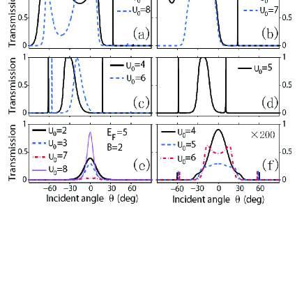
The proposed device relies on the interplay between the Klein tunneling and the wave vector filtering provided by local magnetic fields. To obtain a quantitative understanding of this interplay, Fig. 2 plots the transmission probability calculated as a function of the incident angle for both the P and AP magnetization configurations. In our calculations the structure parameters of the magnetic barrier are set at and . The incident energy is fixed at and the electric barrier height is taken as for different curves.
For the magnetic barrier with P alignment, the transmission spectrum demonstrates obvious angular anisotropy [see Figs. 2(a)-2(d)]. The reflection at normal incidence is finite and is almost complete at suitable electric barrier heights. Instead, perfect transmission appears at some oblique incidences. For example, in the special case , the transmission peak with a finite width locates at [see Fig. 2(d)]. In comparison with the case of pure electric barriers,Klein tunneling3 we can see that the magnetic barrier changes the incident direction at which the Klein tunneling occurs. The transmission is remarkable in a wide region of negative and is blocked by the magnetic barrier when the incident angle exceeds a critical value or is below another critical value . This can be understood as follows. From Eq. (3) we know that evanescent states appear in the magnetic barrier regions when the magnetic vector potential (here ) and electrostatic barrier satisfy . The transmission is generally weak as the decaying length of the evanescent states is shorter than the barrier width. In the transmission forbidden region, there may exist one or two line-shaped peaks with unity values, as a result of resonant tunneling through the symmetric double barrier structure. The applied electric barrier significantly alters the positions of the transmission peaks. We can also observe a large difference between the transmission curves for the barrier height and . Such a difference arises from the fact that the carrier states for the two cases are not completely complementary.
We next examine the transmission characteristics for the AP alignment, which is shown in Figs. 2(e) and 2(f). In this configuration the magnetic vector potential is antisymmetric about the central line [see Fig. 1(c)]. The Dirac Hamiltonian possesses a symmetry associated with the operation , where is the time reversal operator and is the reflection operator . This symmetry implies the invariance of the transmission with respect to the replacement , as seen in Figs. 2(e) and 2(f). For large the transmission decays monotonically as the incident angle increases from zero [see Fig. 2(e)]. Since the carrier states in the two magnetic barriers are not identical, perfect transmission can not be achieved (except for the case of normal incidence). Note that for the AP configuration and a given wave vector , the presence of evanescent states in the first magnetic barrier only requires . When this condition is met for all incident directions and the transmission can be strongly suppressed, as shown in Fig. 2(f). Within this parameter regime, the transmission exhibits a nonmonotonic variation with the positive incident angle. Furthermore, the maximal transmission for the AP alignment can be 2 orders of magnitude lower than that for the P alignment [Figs. 2(c) and 2(d)].
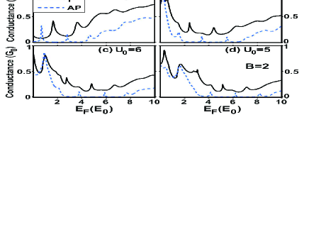
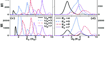
As demonstrated above, the transmission features for the P and AP configurations are quite distinct. Such a difference is also exhibited in the measurable quantity, the conductance . In Fig. 3 the conductance is plotted as a function of the Fermi energy for several heights of the electric barrier. Resonant peaks can be observed in the conductance spectrum for both P and AP alignments. For the P alignment, the conductance is finite (larger than 0.1 in most cases in Fig. 3). For the AP alignment, the conductance is almost zero within a broad energy interval [covering ] except for several sharp conductance peaks. In this energy region is depleted by the magnetic barrier whereas is finite. Away from this transmission-blocking region, essentially increases with the Fermi energy and is primarily contributed by the propagating modes. The normalized difference between and , i.e., the TMR ratio , is presented in Fig. 4(a). In the absence of the electric barrier, high values of are located in the low Fermi energy region, as a result of the strong suppression of transmission in the AP alignment. The inclusion of an electric barrier shifts the transmission-blocking region and, thus, can be used to adjust the MR ratio. The latter is obviously reflected in Fig. 4(b).
In the above analysis, we take simplified magnetic field profiles to illustrate the operating principles of the proposed device. In realistic cases the modulated magnetic field has the smoothing variations on the scale of graphene lattice spacing ( nm). When both FM stripes have the same rectangular cross section and magnetization along the -direction, the generated magnetic field profiles for the P and AP alignments can be obtained analytically.profile For the parameters given in the figure caption the calculated MR ratio is shown in Figs. 4(c) and 4(d). The calculation shows that the conductance of the device has a variation similar to that in Figs. 4(a) and 4(b). The TMR ratio remains large and exhibits rich variations as the electric barrier height increases. Since ferromagnetic elements with a submicron scale have been successfully fabricated on top of a two-dimensional electron systemFM and dielectric layers on monolayered graphene have been realized recently,gate control1 ; gate control2 our considered structure is realizable with current technology.
In summary, we have investigated the transport features of a graphene monolayer under the modulation of both a magnetic double barrier and an electric barrier, where the magnetic double barrier is provided by depositing two parallel ferromagnetic stripes with magnetizations along the current direction. The results indicate that for the AP magnetization configuration the transmission of electrons in graphene can be drastically suppressed for all incident angles. When in the P alignment the Klein tunneling can be generally observed at specific oblique incident directions rather than the normal incidence. The difference of wave-vector-dependent transmission for two magnetization configurations (P/AP) leads to a large TMR ratio, which can be further adjusted by the electric barrier. Note that different thin dielectric layers atop graphene sheets have been fabricated and then the top gates can be formed by means of standard e-beam lithography.gate control1 ; gate control2 The deposition of ferromagnetic materials on insulating layers has been widely adopted to create local magnetic field modulations of the underlying 2D semiconducting systems.magnetic barrier1 ; magnetic barrier2 Thus our proposed device is within the realizable scope of current technological advances.
F. Zhai was supported by the training fund of young teachers at Dalian University of Technology (Grant No. 893208) and the NSFC (Grant No. 10704013). K. Chang was supported by the NSFC (Grant No. 60525405)and the knowledge innovation project of CAS.
References
- (1) K. S. Novoselov, A. K. Geim, D. Jiang, Y. Zhang, S. V. Dubons, I. V. Grogorieva, and A. A. Firsov, Science 306, 666 (2004).
- (2) K. S. Novoselov, A. K. Geim, S. V. Mozorov, D. Jiang, M. I. V. Gregorieva, S. V. Dubonos, and A. A. Firsov, Nature (London) 438, 197 (2005).
- (3) Y. Zhang, Y.-W. Tan, H. L. Stormer, and P. Kim, Nature (London) 438, 201 (2005).
- (4) B. Huard, J. A. Sulpizio, N. Stander, K. Todd, B. Yang, and D. Goldhaber-Gordon, Phys. Rev. Lett. 98, 236803 (2007).
- (5) J. R. Williams, L. DiCarlo, and C. M. Marcus, Sicence 317, 638 (2007).
- (6) V. P. Gusynin and S. G. Sharapov, Phys. Rev. Lett. 95, 146801 (2005).
- (7) V. V. Cheianov and V. I. Falko, Phys. Rev. B 74, 041403 (2006).
- (8) M. I. Katsnelson, K. S. Novoselov, and A. K. Geim, Nature Phys. 2, 620 (2006).
- (9) J. J. Milton Pereira, P. Vasilopoulos, and F. M. Peeters, Appl. Phys. Lett. 90, 132122 (2007).
- (10) A. D. Martino, L. Dell’Anna, and R. Egger, Phys. Rev. Lett. 98, 066802 (2007).
- (11) For recent work, see J. Hong, S. Joo, T.-S. Kim, K. Rhie, K. H. Kim, S. U. Kim, B. C. Lee, and K.-H. Shinc, Appl. Phys. Lett. 90, 023510 (2007); M. Cerchez, S. Hugger, T. Heinzel, and N. Schulz, Phys. Rev. B 75, 035341 (2007) and references therein.
- (12) See, for example, A. Matulis, F.M. Peeters, and P. Vasilopoulos, Phys. Rev. Lett. 72, 1518 (1994); S. J. Lee, S. Souma, G. Ihm, and K. J. Chang, Phys. Rep. 394, 1 (2004).
- (13) H. Xu, Phys. Rev. B 50, 8469 (1994); David Yuk Kei Ko and J. C. Inkson, ibid. 38, 9945 (1988).
- (14) I. S. Ibrahim and F. M. Peeters, Phys. Rev. B 52, 17 321 (1995).
- (15) See, for example, V. Kubrak, F. Rahman, B. L. Gallagher, P. C. Main, H. Henini, C. H. Marrows, and M. A. Howson, Appl. Phys. Lett. 74, 2507 (1999); T. Vančura, T. Ihn, S. Broderick, K. Ensslin, W. Wegscheider, and M. Bichler, Phys. Rev. B 62, 5074 (2000); A. Nogaret, D. N. Lawton, D. K. Maude, J. C. Portal, and M. Henini, ibid. 67, 165317(2003).