Spin current diode based on an electron waveguide with spin-orbit interaction
Abstract
We propose a spin current diode which can work even in a small applied bias condition (the linear-response regime). The prototypal device consists of a hornlike electron waveguide with Rashba spin-orbit interaction, which is connected to two leads with different widths. It is demonstrated that when electrons are incident from the narrow lead, the generated spin conductance fluctuates around a constant value in a wide range of incident energy. When the transport direction is reversed, the spin conductance is suppressed strongly. Such a remarkable difference arises from spin-flipped transitions caused by the spin-orbit interaction.
pacs:
72.25.Dc, 71.70.Ej, 85.75.-d, 73.23.AdThe spin of carriers has been exploited in recent years to develop solid-state devices combining the standard microelectronics with spin-dependent effects.Spintronics ; Spintronics1 The operation of spin-based electronic circuits requires the electrical generation of excess spin in nonmagnetic materials. To this end, various spin injection methods and spin filters have been explored. For a spin filtering device it would be very desirable that the spin polarization (both amplitude and orientation) of the outgoing current could be controllable by electric means.spin filtering diode ; voltage1 ; rectification1 ; rectification2 ; voltage2 ; direction As an example, the concept of spin filtering diodespin filtering diode has been put forward based on the giant Zeeman splitting in semimagnetic semiconductor heterostructures. Its salient feature lies in the large difference of spin polarization when switching the polarity of the dc bias applied to the device. The rectification of spin current has also been predicted in asymmetric systems composed of either a molecular wirerectification1 or a quantum dotrectification2 sandwiched by a ferromagnetic and a nonmagnetic lead. In these systems the ferromagnetic lead is essential to generate a spin-polarized current.
The presence of spin-orbit interaction (SOI) in semiconductors provides a way to design spintronic devices without need for a magnetic element or an external magnetic field. Several devices utilizing multiterminal electron waveguides have been proposed to generate spin-polarized currents by means of the SOI alone.SOC filter1 ; SOC filter2 ; SOC filter3 ; SOC filter4 ; SOC filter5 For a two-terminal stub waveguide structure, we have shown that the SOI-induced effective magnetic field can generate both spin localization inside the stub and spin polarization in the transmitted electron beam near structure-induced Fano resonances.SOC filter6 We have also shown that the SOI alone can not generate a spin-polarized transmitted electron beam in a two-terminal waveguide when the output lead supports only one orbital channel.Zhai-symmetry Inspired by this fact, we will show, in this work, that the spin transport properties of a hornlike waveguide can be utilized to devise a spin current diode without need for a ferromagnetic material or a magnetic field.
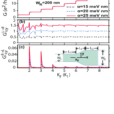
Our system is illustrated in the inset of Fig. 1(c), where a two-dimensional electron gas (2DEG) in the plane is restricted to a waveguide along the direction by a hard-wall confinement potential . The 2DEG is contained in an asymmetric quantum well so that the SOI arises mainly from the interfacial electric field (the Rashba mechanism). The waveguide consists of three parts. The left (right) part has a length () and a uniform width (), connected to the left (right) lead with the same width. A finite difference between the widths of the left and right parts of the waveguide ( and ) is essential for the proposed device. Since we are concerned only with spin-unpolarized injection, the two connecting leads are nonmagnetic and have a vanishing SOI. The central part of the waveguide spans the region , along the direction, within which the waveguide width varies smoothly from the initial value to the final value . To be specific, we take
| (1) |
For simplicity we assume that the whole waveguide shares a common horizontal central line (at ). The effective-mass Hamiltonian describing the considered system reads
| (2) | |||||
Here is the effective mass of electrons, and are the in-plane momentum components, , and are the three Pauli matrices, and is the unit matrix. The Rashba SOI strength is assumed to be uniform (with a value ) in the central part of the waveguide and decreases adiabatically down to zero in the transition regions of the entrance and exit. We take the spin quantum axis to be along the transverse direction, so that and represent the spin-up and spin-down states, respectively.
A real-space discretization of Eq. (2) yields a tight-binding model, which can be solved numerically by means of the recursive Green’s function methodbook to obtain the outgoing wave amplitudes. The Landauer-Büttiker formula is then used to determine the spin-resolved conductances ( or ), which depend both on the incident spin states in one lead and on the outgoing spin states in the other lead. The transmitted spin current in the linear-response regime is characterized by the spin conductance .Zhai-symmetry Since our system is invariant under the operation , where is the reflection , the spin conductance could be nonvanishing only along the direction and is given by
| (3) |
In the calculations we have chosen to fix the size parameters nm and nm. The electron effective mass has been taken to be ( is the free-electron mass), which is appropriate to an InGaAs quantum well system.Sato
In Fig. 1 we plot the total charge conductance and the normalized spin conductance [in unit of ] as functions of the Fermi wave vector , where is the electron Fermi energy, for several values of the SOI strength . Here is given in units of , a value corresponding to the first subband energy in the narrow lead. The charge conductance exhibits a steplike feature [see Fig. 1(a)] and is determined by the number of propagating modes in the narrow lead, . This indicates a negligible backscattering when electrons traverse the considered waveguide structure from the narrow lead to the wide lead (the forward transport direction), that is
| (4) |
The left-to-right and right-to-left charge conductances, and , are identical due to the time reversal symmetry. In contrast, the spin conductance changes remarkably once the transport direction is reversed. Under the forward bias, the spin conductance fluctuates around a single plateau in the whole considered energy region [see Fig. 1(b)]. The plateau moves up as the SOI strength increases. The derivation of from the plateau value occurs in the energy region and near the onset of subbands in the narrow lead. The spin polarization of the current is the ratio between the normalized spin conductance and the normalized charge conductance.Zhai-symmetry As a result, the spin polarization exhibits a steplike decrease as the Fermi energy increases. When electrons are incident from the wide lead, the spin conductance and thus the spin polarization is greatly suppressed [see Fig. 1(c)]. A vanishing spin current is found in the energy region of , in which the outgoing lead (the left lead in this case) can support the lowest orbital mode only. This is in full agreement with the prediction of Ref. Zhai-symmetry, . When the outgoing lead supports two or more propagating orbital modes, the spin conductance can be finite but it is rather small in general [Fig. 1(c)]. A narrow peak is observed near the onset of a subband (with subband index ) of the outgoing lead, which is due to SOI-induced Fano resonance.Fano-Rashba
The contrast in the spin conductance between the forward and backward transport directions indicates a spin current diode even in the small bias condition (the linear-response regime). The spin current of the ”on” state (the forward biased case) can be controlled by the SOI strength. For the ”off” state (the backward biased case), the spin current is weak when the charge conductance is on a quantized plateau or vanishing when the Fermi energy is in the region of . The results can be understood as follows. The spin conductance comes from two parts (). One is the difference between the two spin-conserved conductances () and the other one is the difference between the two spin-flipped conductances (). We first consider the situation that electrons are incident from the left (narrow) lead. From Eq. (4) we know that the two parts, and , are almost identical. Thus, the spin conductance can be expressed in terms of the difference between the two spin-flipped conductances,
| (5) |
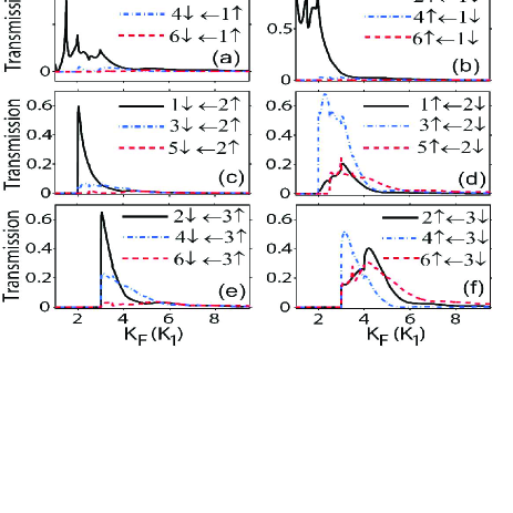
Such a difference is reflected by the variations of spin-flipped transmissions shown in Fig. 2. Here, , while and are the indices of the incident and outgoing modes, respectively. The symmetry of the considered system implies
| (6) |
It can be seen that each nonvanishing transmission is remarkable only within an energy window. When the left lead supports only a single orbital channel [Figs. 2(a) and 2(b)], the spin-flipped transmission for the spin-down injection is much larger than that for the spin-up injection. This can be explained by examining the SOI-induced mode mixing between subbands of different spins in the central part of the considered waveguide.adiabatic As two or more orbital modes are allowable for conducting in the left lead (), can be remarkable and even exceed the corresponding in certain energy windows [see Figs. 2(c)-2(f)]. However, the spin-flipped transmissions for spin-down injections are seen to be in general larger than their corresponding spin-flipped transmissions over large energy regions. Furthermore, there exists such an outgoing channel that is much smaller than . The combination of these facts gives rise to a nearly constant spin conductance.
When the transport direction is reversed, the spin-resolved conductance can be obtained from the relation imposed by the time reversal symmetry,
| (7) |
This relation together with Eq. (4) indicates a cancellation of and and thus results in , as observed in Fig. 1(c). From the above analysis one can see that the spin current diode proposed here relies only on two gradients: the quantized conductance and the difference of the two spin-flipped conductances. Equation (7) also indicates that for a spin-conserved system, such as the system studied in Ref. spin filtering diode, , the diode function of spin current can be performed only in the nonlinear-response regime.
In conclusion, we have proposed a spin current diode based on a waveguide connected to two leads with different width. It is demonstrated that the spin conductance fluctuates around a constant value in a wide range of incident energy when electrons are incident from the narrow lead. When the transport direction is reversed, the spin conductance is suppressed strongly. The rectification of spin current is achievable even in the linear-response regime and thus the proposed diode can work at a low power consumption condition. The SOI alone is utilized to realize such a function of spin current rectification.
F. Zhai was supported by the NSFC (Grant No. 10704013) and the training fund of young teachers at Dalian University of Technology. K. Chang was supported by the NSFC (Grant No. 60525405) and the knowledge innovation project of the Chinese Academy of Sciences. H. Q. Xu acknowledges supports from the Swedish Research Council (VR) and from the Swedish Foundation for Strategic Research (SSF) through the Nanometer Structure Consortium at Lund University.
References
- (1) S. A. Wolf, D. D. Awschalom, R. A. Buhrman, J. M. Daughton, S. von Molnár, M. L. Roukes, A. Y. Chtchelkanova, and D. M. Treger, Science 294, 1488 (2001).
- (2) I. Zutic, J. Fabian, and S. D. Sarma, Rev. Mod. Phys. 76, 323 (2004).
- (3) Y. Guo, X. Y. Chen, F. Zhai, B. L. Gu, and Y. Kawazoe, Appl. Phys. Lett. 80, 4591 (2002); F. Zhai, Y. Guo, and B. L. Gu, J. Appl. Phys. 94, 5432 (2003).
- (4) A. Slobodskyy, C. Gould, T. Slobodskyy, C.R. Becker, G. Schmidt, and L.W. Molenkamp, Phys. Rev. Lett. 90, 246601 (2003).
- (5) H. Dalgleish and G. Kirczenow, Phys. Rev. B 73, 235436 (2006).
- (6) F. M. Souza, J. C. Egues, and A. P. Jauho, Phys. Rev. B 75, 165303 (2007).
- (7) F. Zhai and H.Q. Xu, Phys. Lett. A 369, 498 (2007).
- (8) T. Kimura, Y. C. Otani, and P. M. Levy, Phys. Rev. Lett. 99, 166601 (2007).
- (9) A. A. Kiselev and K. W. Kim, Appl. Phys. Lett. 78, 775 (2001).
- (10) M. Governale, D. Boese, U. Zülicke, and C. Schroll, Phys. Rev. B 65, 140403(R) (2002).
- (11) J. Ohe, M. Yamamoto, T. Ohtsuki, and J. Nitta, Phys. Rev. B 72, 041308(R) (2005).
- (12) M. Yamamoto, T. Ohtsuki, and B. Kramer, Phys. Rev. B 72, 115321 (2005).
- (13) A. W. Cummings, R. Akis, and D. K. Ferry, Appl. Phys. Lett. 89, 172115 (2006).
- (14) F. Zhai and H. Q. Xu, Phys. Rev. B 76, 035306 (2007).
- (15) F. Zhai and H. Q. Xu, Phys. Rev. Lett. 94, 246601 (2005).
- (16) D. K. Ferry and S. M. Goodnick, Transport in nanostructures (Cambridge University Press, Cambridge, 1997).
- (17) Y. Sato, T. Kita, S. Gozu, and S. Yamada, J. Appl. Phys. 89, 8017 (2001).
- (18) Lebo Zhang, P. Brusheim, and H. Q. Xu, Phys. Rev. B 72, 045347 (2005); D. Snchez and L. Serra, Phys. Rev. B 74, 153313 (2006); Lebo Zhang, F. Zhai, and H. Q. Xu, Phys. Rev. B 74, 195332 (2006).
- (19) M. Eto, T. Hayashi, and Y. Kurotani, J. Phys. Soc. Jpn. 74, 1934 (2005).
Figure Captions