Electronic Structures of SiC Nanoribbons
Abstract
Electronic structures of SiC nanoribbons have been studied by spin-polarized density functional calculations. The armchair nanoribbons are nonmagnetic semiconductor, while the zigzag nanoribbons are magnetic metal. The spin polarization in zigzag SiC nanoribbons is originated from the unpaired electrons localized on the ribbon edges. Interestingly, the zigzag nanoribbons narrower than 4 nm present half-metallic behavior. Without the aid of external field or chemical modification, the metal-free half-metallicity predicted for narrow SiC zigzag nanoribbons opens a facile way for nanomaterial spintronics applications.
pacs:
73.22.-f, 73.61.WpI INTRODUCTION
Stimulated by the successful preparation of graphene, an intense research interest has been focused on two dimensional (2D) layered structures. Among several group IV elements, only carbon can take either or bond configurations and form 2D layered structure. Silicon prefers instead of hybridization. As a result, it is difficult to construct stable Si structures of fullerenes, nanotubes, and graphene-like sheets. Khan However, it is possible to form layered structure by mixing C and Si. Recently, SiC single-wall nanotubes (SWNTs) with different chiralities, diameters, and atomic configurations have been studied by first principles calculations, Miyamoto ; Menon ; Zhao ; Gali ; Baumeier ; Baierle1 ; Baierle2 and synthesized experimentally via the reaction of silicon with multiwalled carbon nanotubes at different temperatures. Sun In contrast to carbon SWNTs, SiC SWNTs are always semiconducting independent of the helicity, with a direct band gap for zigzag tubes and an indirect gap for armchair and chiral tubes. It is suggested that SiC SWNTs are candidates for nanodevices that operate in high-power, high-frequency and high-temperature regimes. Harris ; Pan ; Feng
Nanoribbon (NR) is an important structure for 2D layered materials. Graphene NRs have been extensively studied in the last two years. Fujita ; Yuanbozhang ; Berger ; Son1 ; Son2 ; NL07 ; APL-kaner ; Jiang07 ; JACS-kaner ; ZuanyiLi-PRL The hydrogen passivated graphene NRs have a nonzero band gap. The zigzag graphene NRs have a magnetic insulating ground state with ferromagnetic ordering at each zigzag edge and antiparallel spin orientation between the two edges. Son1 Transverse electric field or chemical decoration turn zigzag graphene NRs to half metal, which makes them good candidates for spintronics applications. Son2 ; APL-kaner ; JACS-kaner However, metal-free half-metallicity has not been obtained without the aid of external field or chemical modification.
In this paper we study the geometric and electronic structures of SiC NRs based on density functional theory (DFT). Spin-polarized calculations are performed to explore possible magnetic ordering. The width effects on the properties of SiC NRs are carefully studied. Half-metallicity is predicted for narrow zigzag SiC NRs. The stability of SiC NRs are also discussed.
II COMPUTATIONAL METHOD AND MODEL SYSTEM
First principles calculations were performed using the Vienna ab initio simulation package (VASP). vasp_1 ; vasp_2 We described the interaction between ions and electrons using the projector augmented wave (PAW) approach. PAW_1 ; PAW_2 The Perdew-Wang functional (PW91) under the generalized gradient approximation (GGA) was used to describe the exchange correlation interaction. PW91_1 ; PW91_2 During the structure optimizations, all atoms were fully relaxed until the Hellmann-Feynman forces acting on them smaller than 0.01 eV/Å. For nanoribbons, the Brillouin-zone integrations were performed on a 1111 Monkhorst-Pack grid. Monkhorst 120 uniform -points along the one dimensional Brillouin zone were used to obtain the band structures of the SiC NRs. The periodic boundary condition was set with the vacuum region between two neighboring ribbons larger than 10 Å. The phonon band structures were calculated with the general utility lattice program (GULP) Gale1 ; Gale2 using the Tersoff force field. Tersoff_1 ; Tersoff_2
III RESULTS and DISCUSSION
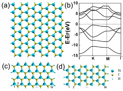
Before studying the properties of nanoribbons, we first check the two-dimensional hexagonal SiC sheet. The optimized structure is shown in Fig. 1a, and the obtained Si-C bond length is 1.787 Å. The electronic band structure shown in Fig. 1b presents a direct energy gap of 2.55 eV at the K point in the hexagonal Brillouin zone, as expected, which is narrower than the result obtained by self-interaction corrected DFT calculation. Baumeier An accurate first-principles calculation of band gaps requires a quasiparitcle approach. The basic physics discovered here however should not be changed.
Similar to graphene NRs Son1 , we consider two types of SiC NRs with armchair and zigzag shape edges, as shown in Fig. 1c and 1d, respectively. The nanoribbon width W is defined as the number of dimer lines along the ribbon direction for an armchair SiC NR and the number of zigzag chains for a zigzag SiC NR. All dangling bonds at the ribbon edges are saturated by hydrogen atoms. The optimized Si-H and C-H bond lengths are 1.49 and to 1.09 Å, respectively.
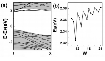
The band structures for armchair SiC NRs with different widths are all similar. As an example, the W=11 band structure is plotted in Fig. 2a. There is a direct band gap at the point. As shown in Fig. 2b, the variation of the energy gap as a function of ribbon width W exhibits a three-family behavior, which is similar to the graphene NRs Son1 . The main difference between these two types of armchair NRs is that the energy gap increases with the ribbon width for SiC NRs, while it decreases for graphene NRs. Secondly, we have >> for SiC NRs compared to >> for graphene NRs.
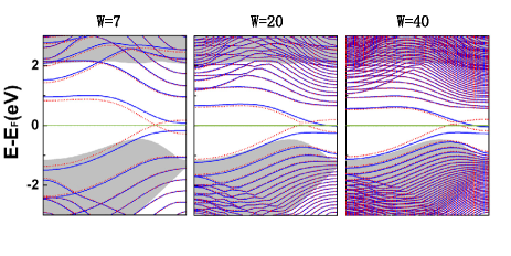
For zigzag SiC NRs, we first check the band structure of the W=7 NR, as shown in Fig. 3. There are four bands close to the Fermi level. The two bands in the spin-up channel cross each other, and both cross the Fermi level. Therefore, the spin-up energy gap is zero. In the spin-down channel, the two bands close to the Fermi level form a direct gap at the point. We name the higher of these two bands as , the lower as , and the gap between them as . When W=7, the band is totally unoccupied, and the band is totally occupied. The spin-down energy gap is thus equal to , i. e. 0.25 eV. And the zigzag SiC NR with W=7 presents a half-metallic electronic structure.
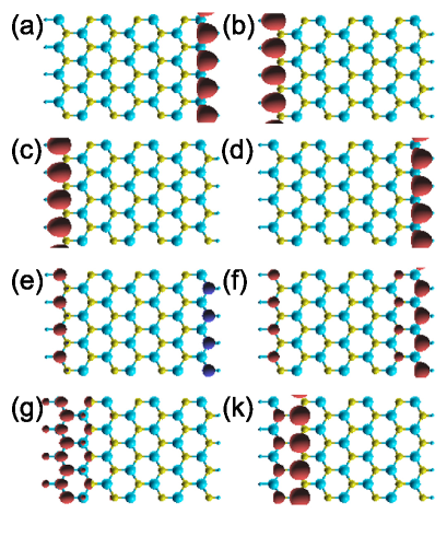
The four bands close to the Fermi level are not totally covered by the projected band structure of the two-dimensional SiC sheet, which strongly suggests the edge state characters of these four bands. As shown in Fig. 4, at the point, all the four bands close to the Fermi level correspond to edge states.
There are local magnetic moments on the edge atoms, and their orientation are antiparallel between the two edges (Fig. 4e). However, we note that the net magnetic moments in a unit cell is not zero (refer to table 1). Therefore, the two edges are not antiferromagnetically coupled as in zigzag graphene NRs, and they are ferrimagnetically coupled. To consider the charge transfer between the two edge, we plot the partial charge density from the valence band maximum of the two dimensional SiC sheet to the Fermi level in Fig. 4f. We can clearly see a charge transfer from the Si edge to the C edge.
As shown in Table 1, the band gap between the and bands () decreases with the increase of the ribbon width. We also observed the sink of the band minimum at the point with the increase of ribbon widths. When W larger than 20, the band cross with the Fermi level, and the energy gap in the spin-down channel close. The nanoribbons thus turn to metal from half metal. In the spin-up channel at the point, the occupied state comes from the Si edge, and the unoccupied state comes from the C edge, which is opposite to the spin-down channel. The band cross in the spin-up channel leads to a net electron transfer from the Si edge to the C edge. Therefore, the sink of the band at the point decrease the charge polarization between the two edges. This is consistent with our previous study BCN on the CBN nanoribbon: the charge polarization decreases when the ribbon width increases.
| W | ||||||||
|---|---|---|---|---|---|---|---|---|
| (eV) | 0.39 | 0.34 | 0.25 | 0.24 | 0.24 | 0.24 | 0.085 | |
| 0.020 | 0.023 | 0.033 | 0.042 | 0.048 | 0.051 | 0.059 |
We note that the two dimensional SiC sheet is an insulator with a big gap. However, for zigzag SiC nanoribbon with W as large as 40, we still get metallic band structure. For armchair SiC nanoribbons, as shown in Fig. 2 our calculated band gaps also converge to a value smaller than the bulk gap (2.55 eV). This is due to the edge states. Similar behavior has been observed for boron nitride nanoribbons. BN There are many bands outside the projected band structure of two dimensional SiC sheet. In Fig. 4, we plot the density of the +1 band at the and point. Although they are not edge states, they are localized on part of the ribbon.
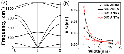
To develop applications for SiC NRs, it is important to study their stability. First, we calculate the phonon band structures of the two dimensional SiC sheet. As shown in Fig. 5, there is no imaginary frequency exists. The calculated frequency of the highest optical phonon at point is 1378.5 cm-1. For SiC NRs and corresponding nanotubes, we define the Gibbs free energy of formation as a function of the chemical potential of the silicon carbide and hydrogen species.
| (1) |
where is the cohesive energy per atom, and are the mole fraction and the chemical potential of silicon carbide (hydrogen), respectively. is set to half of the energy of H2. is the conhensive energy per Si-C unit of infinite two dimensional SiC sheet. Therefore, the of 2D SiC sheet is zero by definition. The comparison of between SiC NRs and NTs with the same numbers of Si and C atoms are shown in Fig. 5. We can see that there is a crossover between the SiC NRs and the SiC NTs. The narrower zigzag SiC NRs are even more stable than the corresponding NTs.
IV CONCLUSIONS
In conclusion, We have investigated the electronic and magnetic properties of SiC NRs with armchair and zigzag shaped edges. We show that the armchair SiC NRs always have a wide band gap for all width. The zigzag SiC NRs with the width smaller than nm present half metallic behavior. This makes narrow zigzag SiC nanoribbon a great candidate for spintronics application, since neither transverse electric field nor chemical modification is needed to obtain half-matallicity. The Gibbs free energy of formation of SiC NRs are similar to that of previously studied SiC NTs, narrow nanoribbons are even more stable than the experimentally synthesized SiC nanotubes, which suggests it is practical to synthesize SiC nanoribbons.
Acknowledgements.
This work was partially supported by the National Natural Science Foundation of China under Grand Nos. 10674121, 20533030, 10574119, and 50121202, by National Key Basic Research Program under Grant No. 2006CB922004, by the USTC-HP HPC project, and by the SCCAS and Shanghai Supercomputer Center.References
- (1) F. Khan, J. Broughton, Phys. Rev. B 43, 11754 (1991).
- (2) Y. Miyamoto and B. D. Yu, Appl. Phys. Lett. 80, 586 (2002).
- (3) M. Menon, E. Richter, A. Mavrandonakis, G. Froudakis, and A. N. Andriotis, Phys. Rev. B 69, 115322 (2004).
- (4) M. Zhao, Y. Xia, F. Li, R. Q. Zhang, and S.-T. Lee, Phys. Rev. B 71, 085312 (2005).
- (5) A. Gali, Phys. Rev. B 73, 245415 (2006).
- (6) Bjrn Baumeier, Peter Krger, and Johannes Pollmann, Phys. Rev. B 76, 085407 (2007).
- (7) R. J. Baierle, P. Piquini, L. P. Neves, and R. H. Miwa, Phys. Rev. B 74, 155425 (2006).
- (8) R. J. Baierle, R. H. Miwa, Phys. Rev. B 76, 205410 (2007).
- (9) X. H. Sun, C. P. Li, W. K. Wong, N. B. Wong, C. S. Lee, S. T. Lee, and B. K. Teo, J. Am. Chem. Soc. 124 14464 (2002).
- (10) Properties of Silicon Carbide, edited by G. L. Harris (INSPEC, Institution of Electrical Engineers, London, 1995).
- (11) Z. Pan, H.-L. Lai, F. C. K. Au, X. Duan, W. Zhou, W. Shi, N. Wang, C-S. Lee, N.-B. Wong, S.-T. Lee, and S. Xie, Adv. Mater. (Weinheim, Ger.) 12, 1186 (2000).
- (12) Z. C. Feng, A. J. Mascarenhas, W. J. Choyke, and J. A. Powell, J. Appl. Phys. 64, 3176 (1998).
- (13) M. Fujita, K. Wakabayashi, K. Nakada, and K. Kusakabe, J. Phys. Soc. Jpn. 65, 1920 (1996).
- (14) Y. Zhang, Y. Tan, H. L. Stormer, and P. Kim, Nature (London) 438, 201 (2005).
- (15) C. Berger, Z. Song, X. Li, X. Wu, N. Brown, C. Naud, D. Mayou, T. Li, J. Hass, A. N. Marchenkov, E. H. Conrad, P. N. First, and W. A. de Heer, Science 312, 1191 (2006).
- (16) Y. W. Son, M. L. Cohen, and S. G. Louie, Phys. Rev. Lett. 97, 216803 (2006).
- (17) Y. W. Son, M. L. Cohen, and S. G. Louie, Nature 444, 347-349 (2006).
- (18) O. Hod, V. Barone, J. E. Peralta, and G. E. Scueria, Nano Lett. 7, 2295(2007).
- (19) E. J. Kan, Z. Li, J. Yang, and J. G. Hou, Appl. Phys. Lett. 91, 243116(2007).
- (20) Jiang, D. E.; Sumpter, B. G.; Dai, S. J. Chem. Phys. 126, 134701 (2007).
- (21) E. J. Kan, Z. Li, J. Yang, and J. G. Hou, J. Am. Chem. Soc. 130, 4224(2008).
- (22) Z. Li, H. Y. Qian, B. L. Gu, and W. H. Duan, Phys. Rev. Lett. 100, 206802 (2008).
- (23) G. Kresse and J. Hafner, J. Phys.: Condens. Matter, 6, 8245 ( 1994).
- (24) G. Kresse and J. Hafner, Phys. Rev. B 49, 14251 (1994).
- (25) P. E. Blchl, Phys. Rev. B 50, 17953 (1994).
- (26) G. Kresse and D. Joubert, Phys. Rev. B 59, 1758 (1999).
- (27) J. P. Perdew and Y. Wang, Phys. Rev. B 45, 13244 (1992).
- (28) J. P. Perdew, J. A. Chevary, S. H. Vosko, K. A. Jackson, M. R. Pederson , D. J. Singh and C. Fiolhais, Phys. Rev. B 46, 6671 (1992).
- (29) H. J. Monkhorst and J. D. Pack, Phys. Rev. B 13, 5188 (1976).
- (30) D. J. Gale, Chem. Soc., Faraday Trans. 93, 629 (1997).
- (31) D. Gale, A. L. Rohl, Mol. Simul. 29, 291 (2003).
- (32) J. Tersoff, Phys. Rev. Lett. 56, 632 (1986).
- (33) J. Tersoff, Phys. Rev. B. 37, 6991 (1988).
- (34) E.-J. Kan, X. Wu, Z. Li, X. C. Zeng, J. Yang, J. G. Hou, http://arxiv.org/abs/0803.2073.
- (35) C.-H. Park, S. G. Louie, Nano Lett. (2008) DOI: 10.1021/nl080695i.