Tunable Graphene System with Two Decoupled Monolayers
Abstract
The use of two truly two-dimensional gapless semiconductors, monolayer and bilayer graphene, as current-carrying components in field-effect transistors (FET) gives access to new types of nanoelectronic devices. Here, we report on the development of graphene-based FETs containing two decoupled graphene monolayers manufactured from a single one folded during the exfoliation process. The transport characteristics of these newly-developed devices differ markedly from those manufactured from a single-crystal bilayer. By analyzing Shubnikov-de Haas oscillations, we demonstrate the possibility to independently control the carrier densities in both layers using top and bottom gates, despite there being only a nano-meter scale separation between them.
pacs:
73.23.-b, 81.07.-b, 73.43.-fThe development of the micromechanical cleavage technique for
manufacturing ultra-thin graphitic films has made it possible to
produce FETs based upon monolayer graphene and to study their
electronic properties Novoselov2004 ; Novoselov2005 ; kim_nature ; Rise
indicating that graphene is a gapless
semiconductor with a peculiar Dirac-type spectrum of charge
carriers. Using micromechanical exfoliation, multilayers of
graphene are also often produced. Two layers of graphene prepared
by exfoliation usually exhibit crystalline ordering with a
characteristic AB stacking Novoselov2006 ; bilayer_mccann ,
later referred to as single-crystal (SC) bilayer. This should be
contrasted to pairs/stacks of individual misoriented graphene
flakes identified among some of the peeled graphitic films using
Raman spectroscopy raman_misoriented and in multilayers
grown epitaxially on SiC multi_single_epitax_haas . While
the individual carrier density in such layers is usually beyond
experimental control, in this paper we report on the realisation
of two-layer graphene-based FETs where the density on the two
monolayers can be varied separately, despite them lying only a
dozen Angstroms
apart.
The nanostructures presented in this letter were prepared by peeling off pieces from natural bulk graphite graphit with adhesive tape and placing them on a silicon wafer covered with SiO2. Since, at the intermediate stage of the utilized deposition process only some part of the graphene flake touches the SiO2 surface, the flake flips over during the removal of the adhesive tape, thus producing two misoriented graphene layers lying on top of each other and separated by occasional surface deposits (Fig. 1a sketches the top-view of such a structure).
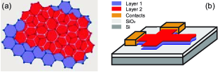
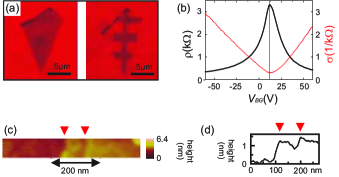
Then, this material is processed into Hall-bar samples using plasma etching and contacted (to both layers) by evaporating chromium and gold electrodes (Fig. 1b). Figure 2a shows two optical images of such a sample before and after plasma etching. A darker than other areas top-left edge indicates the position of the fold. Scanning the structure with an atomic force microscope (AFM) reveals a double step at the etched edges (Fig. 2c and d) with a first-step height of 1.1 nm. Although layers of graphene should have a height of 0.34 nm, previous AFM measurements showed values up to 1 nm for single layer graphene lying on a substrate Novoselov2004 attributed to a water layer underneath graphene and/or the rippling graphene surface.
From these data and also from the transport measurements shown below we conclude that
the first step is due to a monolayer of graphene. The second step
has a height of 0.6 nm which is larger than the thickness of one
layer but less than the height of two AB stacked layers. This
indicates that the second layer is also a single layer which is
separated further from the first layer than in a conventional
bilayer.
To distinguish the designed device from monolayers or SC bilayers we performed transport measurements on the sample shown in Fig. 2, applying magnetic fields up to 13 T at temperatures down to 1.5 K. To reduce the influence of contact resistance on the measurements, a multi-terminal device has been used, and different combinations of two and three point measurements were performed at a broad range of back-gate voltage, V V, applied between the substrate of n-Si and graphene. As usual, positive back-gate voltage induces electrons, negative holes. Figure 2b shows the measured field effect on graphene resistivity demonstrating the operation of the device as an FET Novoselov2004 . A characteristic peak in the observed resistivity points at the approximate neutrality condition for the graphene layers, which is shifted to a finite back-gate voltage V indicating natural doping of the graphene flakes. The measured maximum resistivity, k at 1.5 K, is about half of the earlier-reported typical values for monolayers Novoselov2005 ; Rise , which is in line with the assumption that the device consists of two monolayers conducting in parallel.
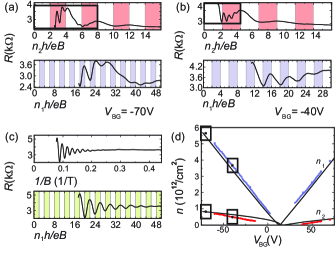
Most importantly, the layer structure of ultrathin graphitic films can be characterized by analyzing the Shubnikov-de Haas (SdH) oscillations in the flake resistance studied as a function of a magnetic field applied perpendicular to the sample. The Berry’s phase characteristic of electrons in monolayer graphene is directly related to the appearance of SdH oscillations minima at filling factors Novoselov2005 ; kim_nature , in contrast to SC bilayer graphene bilayer_mccann where the electron’s Berry’s phase is and the SdH oscillations minima appear at filling factors , with being the filling factor, the carrier concentration, and an integer. When studied at a fixed back-gate voltage (e.g. V and V, Fig 3a,b), the magnetoresistance measured in the two-layer device and plotted versus displays oscillations with two very different periods (compared in detail in the top/bottom panels of Fig. 3 a,b) manifesting the co-existence of two very different carrier densities, and in the sample. These two density values can be obtained from the period of the SdH oscillations, as (where we take into account both the spin and valley degeneracy in the graphene band structure). Their experimentally determined gate-voltage dependence is shown in Fig. 3d. Systematically repeated at all the studied voltage values, the periodicity of both fast (lower panel) and slow (upper panel) -oscillations in the two-layer structure was such that the resistivity minima could only be attributed to the sequence of filling factors , which is typical for monolayer graphene.
To highlight this behavior of the presented data, in the top/bottom panels of Fig 3a,b the intervals with the rising parts of the corresponding oscillations are colored in red/blue. For comparison, Fig. 3c shows the results of a similar study performed for a SC bilayer, where the sequencing of the SdH oscillations minima coincides with the earlier observed Novoselov2006 appearance of maxima at filling factors specific for such a material. Finally, the observed carrier densities and in the two-layer device and their dependence on back-gate voltage presented in Fig. 3d can be compared to theoretically calculated values plotted on the same figure as black lines. The presented calculation takes into account the electrostatics of the device containing two monolayers at distance nm from each other lying on top of the SiO2 dielectric layer (with permittivity and thickness ), Fermi-energy dependence of the compressibility of the electron gas with the Dirac spectrum , and additional doping charge, cm-2 due to deposits left on top of the upper layer in the course of the manufacturing process.
The parameters used in this calculation were obtained by fitting the observed -dependence with the analytical result relating the two densities on two parallel graphene flakes,
where the first equation states the equivalence of the
electro-chemical potentials on the two graphene layers with , whereas the second relates the total charge density in
the device to its electrostatic capacity.
To tune the two carrier densities independently on the two
parallel layers, we fabricated a two-layer sample with an
additional top gate. A schematic view of the manufactured device
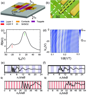
is shown in Fig. 4a, with the design resembling that of the
top-gated SC bilayer structures used recently Morpurgo2007 .
To fabricate the top gate, polymethylmethacrylat (PMMA) was spun
onto a Hall-bar device which was produced in a similar way as the
sample shown in Fig. 2. The PMMA layer was partially exposed to an
electron beam converting the PMMA into a layer insoluble by
acetone. Putting the sample in an acetone bath leaves an
insulating PMMA layer of about 60 nm on top of the graphene flake.
A local top gate with an area of m2 was fabricated on
top of this PMMA layer using standard electron beam lithography.
Figure 4b shows an image of the top-gated sample. The resistance
measured in this device as a function of the back-gate voltage for
a fixed top-gate voltage, is shown in Fig. 4c (for
V). Its back-gate voltage dependence contains two
pronounced peaks (marked by arrows) indicating the difference
between the carrier concentrations in the top-gated and free parts
of the device. The back-gate voltage interval between the two
peaks corresponds to the bipolar transistor regime, with a p-n-p
junction Falko_PhysRev formed underneath the top gate
C_Marcus_Science ; P_Kim_PRL . The tunability of the device
using the top gate is demonstrated in Fig. 4d. Here, the back-gate
voltage was kept fixed at V and the top-gate voltage,
was varied. Due to the large negative back-gate voltage,
the resistance maximum corresponding to the ’neutrality point’ in
the top-gated region appears at positive voltage V (not
shown in the figure). To improve the visibility of the SdH
oscillations and their evolution with , we differentiate
the device’s resistance with respect to the magnetic field value
and show the result using the blue-scale plot in Fig. 4d where one
sees several sets of oscillations. The oscillations which are
almost independent of the top-gate voltage originate from the
areas outside the top-gated region. The oscillations with a strong
dependence characterize the layers underneath the top
gate. The deconvolution of these two contributions is achieved by
the numerical subtraction of the independent part of the
resistance. The resulting magnetooscillations are shown in Figs.
4e,f as function of filling factor for V and
V. Similarly to the first two-layer device, the
top-gated structure shows the superposition of two monolayer-type
SdH oscillations with different periods corresponding to densities
cm-2 and cm-2 for V and V, and to
cm-2 and cm-2 for V and V. This
demonstrates not only that the different carrier densities on the
two closely laid graphene layers can be detected, but also that
those densities can be independently controlled and tuned using a
combination of top/backgates.
In conclusion, we demonstrated the realization of a graphene-based field-effect transistor containing two decoupled graphene monolayers at a nanometer distance from each other. Using the magnetotransport measurements, we determine the carrier densities on the two parallel layers and show the ability to control those densities separately using a combination of electrostatic (back & top) gates. When operated in a broad voltage range, such a device could be employed in a search for the recently predicted superfluidity Min2008 in the ’excitonic insulator’ state expected to form in a pair of graphene layers with opposite polarity. Also, the technique of layer folding offers a promising method for making devices with separately contacted pairs of monolayers acting as atomically-thin optically-transparent Abergel2007 ; GeimOptics electrodes to study vertical transport and electro-optical characteristics of nanoparticles of various materials that can be captured between them.
The authors acknowledge financial support by the excellence cluster QUEST within the German Excellence Initiative. V. F. thanks the A. von Humboldt Foundation for hospitality. This work was supported by ESF grant SpiCo, EPSRC-Lancaster Portfolio Partnership grant, and EPSRC.
References
- (1) K. S. Novesolelov, A. K. Geim, S. V. Morozov, D. Jiang, Y. Zhang, S. V. Dubonos, I. V. Grigorieva, and A. A. Firsov, Science 306, 666 (2004).
- (2) K. S. Novoselov, A. K. Geim, S. V. Morozov, D. Jiang, M. I. Katsnelson, I. V. Grigorieva, S. V. Dubonos, and A. A. Firsov, Nature 438, 197 (2005).
- (3) Y. Zhang, Y. W. Tan, H. L. Stormer, and P. Kim, Nature 438, 201 (2005).
- (4) A. K. Geim and K. S. Novoselov, Nature Materials 6, 183 (2007).
- (5) K. S. Novoselov, E. McCann, S. V. Morozov, V. I. Fal ko, M. I. Katsnelson, U. Zeitler, D. Jiang, F. Schedin, and A. K. Geim, Nature Physics 2, 177-180 (2006).
- (6) E. McCann and V. I. Fal’ko, Physical Review Letters 96, 086805 (2006).
- (7) P. Poncharal, A. Ayari, T. Michel, and J. -L. Sauvajol, arXiv 0805.0511v1 (2008).
-
(8)
J. Hass, F. Varchon, J. E. Milla n-Otoya, M. Sprinkle, N. Sharma, W. A. de Heer, C. Berger, P. N. First, L. Magaud, and E. H. Conrad, Physical Review Letters 100, 125504 (2008).
- (9) NGS Naturgraphit GmbH.
- (10) J. B. Oostinga, H. B. Heersche, X. Liu, A. F. Morpurgo, and L. M. K. Vandersypen, Nature Materials 7, 151 (2008).
- (11) V. V. Cheianov and V. I. Fal’ko, Physical Review B 74, 041403 (2006).
- (12) B. Oezyilmaz, P. Jarillo-Herrero, D. Efetov, D. A. Abanin, L. S. Levitov, and P. Kim, Physical Review Letters 99, 166804 (2007).
- (13) J. R. Williams, L. DiCarlo, and C. M. Marcus, Science 317, 638 (2007).
- (14) H. Min, R. Bistritzer, J.-J. Su, and A. H. MacDonald, arXiv: 0802.3462v1 (2008).
- (15) D. Abergel, A. Russell, and V. I. Fal’ko, Applied Physics Letters 91, 063125 (2007).
- (16) R. R. Nair, P. Blake, A. N. Grigorenko, K. S. Novoselov, T. J. Booth, T. Stauber, N. M. R. Peres, and A. K. Geim, Science 320, 1308(2008).