Time-dependent single electron tunneling through a shuttling nano-island
Abstract
We offer a general approach to calculation of single-electron tunneling spectra and conductance of a shuttle oscillating between two half-metallic leads with fully spin polarized carriers. In this case the spin-flip processes are completely suppressed and the problem may be solved by means of canonical transformation, where the adiabatic component of the tunnel transparency is found exactly, whereas the non-adiabatic corrections can be taken into account perturbatively. Time-dependent corrections to the tunnel conductance of moving shuttle become noticeable at finite bias in the vicinity of the even/odd occupation boundary at the Coulomb diamond diagram.
I Introduction
Single electron tunneling (SET) is a salient feature of quantum transport in nanostructures. The SET phenomenon is observed in various systems, e.g. quantum dots in a tunnel contact with metallic electrodes, Pugla05 ; Cowre molecular bridges between the edges of broken metallic wires, Park ; Yu ; Roch atoms and molecules absorbed on metallic surfaces in a contact with the tip of tunnel microscope, Bode ; Otte etc. The study of electron tunneling through the nano-object with time-dependent characteristics is one of the most challenging problems in this field.
There are several sources of time dependence, which may be realized in practical devices. The simplest one is the time-dependent gate voltage applied to the dot. It is well known GA ; KNG ; KKAR that this time dependence may be converted into the time dependence of tunnel matrix element. Another possibility is the nanoelectromechanical shuttling (NEMS),shut where the nano-size island suspended on a pivotpivot or attached to a stringKoenig oscillates between the leads under the action of an electro-mechanical force. In case of molecular bridges, the vibration eigen modes may be the source of the periodical oscillations of tunneling parameters.Has ; Roch
Usually the tunneling between metallic leads and such a nanoobject is accompanied by many-particle Kondo screening effect GR ; Ng resulting in specific type of zero-bias anomaly (ZBA) in tunnel conductance. Modification of Kondo regime because of periodically modulated in time tunneling rate due to the center-of-mass oscillations was studied recently in several papers. If the oscillations are the eigen modes of a nanoobject (molecule), then the Kondo-peak (zero bias anomaly in tunnel conductance) may transform into dip due to the destructive interference with vibrational mode. Has In case of adiabatic motion induced by electromechanical forces (NEMS) shut the Kondo temperature follows the periodical evolution of the dot position and increases eventually due to effective reduction of the average distance between the dot and the leads, KKSV which is determined by the mean square displacement of the dot (in analogy with Debye-Waller effect in scattering intensity). Non-adiabatic enhancement of Kondo tunneling through such moving nanoobject at finite source-drain bias has been studied recently.Gok
In the present paper we consider adiabatic and non-adiabatic time-dependent effects in conventional cotunneling between metallic leads due to periodic modulation of lead-dot tunneling rate. To suppress many-particle Kondo screening effects, one should consider leads with magnetically polarized electrons. The tunneling between the ferromagnetically ordered leads was discussed recentlyMart1 ; Bulka ; Lopa02 ; Choi ; Tan04 ; Chin08 ; Pas in the context of Kondo effect. We are interested in the situation, where the spin-flip cotunneling is completely suppressed at small lead-dot bias and low temperatures. Such tunneling regime may be realized in half-metallic ferromagnets, where the Fermi surface is formed only by the majority spin electrons, whereas the spectrum of minority spin carries is gapped. The electronic and magnetic properties of such metallic compounds are reviewed in Ref. Kats, . From the point of view of existing devices, where the leads are formed by two-dimensional electrons in degenerate semiconductors, the relevant material for our studies is dilute magnetic semiconductor (Ga,Mn)As.Jung The indirect magnetic exchange between Mn impurity ions is responsible for the long-range ferromagnetic order in this material. This exchange is mediated by spin-polarized carriers near the top of the valence band. The tunnel current in the half-metallic regime arises due to the minority spin hole cotunneling.
We will show that in the absence of Kondo effect the problem of tunneling through moving nano-island (quantum dot) may be solved by means of time-dependent canonical transformation, which exactly takes into account both adiabatic and non-adiabatic lead-dot tunneling processes diagonal in the lead indices. The non-diagonal source-drain cotunneling may be treated by the canonical transformation method only perturbatively, but the adiabatic and non-adiabatic contributions into tunnel conductance may be sorted out also in this case. It will be shown that the time-dependent contribution into current-voltage characteristics of moving nano-object is significant near the boundaries of Coulomb diamonds.
II Model
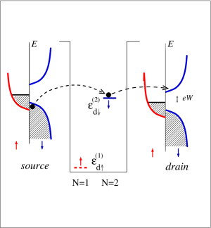
We choose for the realization of ac-driven tunnel conductivity the simplest model of a nanoobject, which is widely used in the studies of single-electron tunneling (SET). A nanoobject is represented in this model by the quantum well with resonance level (see Fig. 1, upper panel). The SET regime arises due to the Coulomb blockade effect: addition energy for the second electron in a singly occupied dot is , where is the tunneling rate to the left () and right ()lead, and is the capacitive energy of the dot. To separate the time-dependent SET from the Kondo ZBA, we consider tunneling between spin-polarized leads, where spin-flip processes are inelastic, because the continuum of electron-hole pairs with the opposite spins in the leads responsible for the Kondo effect is gapped. Two types of spin polarized (magnetically ordered) metallic leads are presented schematically in Fig. 1. In the middle panel the leads are formed by ”half-metallic ferromagnets”Kats with gapped spectrum of minority spin carries. In the lower panel characteristic for -type degenerate dilute magnetic semiconductorsJung the carriers are the minority spin holes.
Virtual tunneling results in a shift of level positions in QD. This renormalization (”Friedel shift”) is also spin dependent. As a result the spin polarization of QD adjusts to that of the ferromagnetic lead (see calculations below). All Kondo processes are quenched in this regime.

The Anderson Hamiltonian modeling SET has the form
| (1) |
where the terms
| (2) |
describe the electron states in the isolated dot and two metallic (semiconductor) leads, respectively. We write in terms of its eigenstates (Hubbard representation). This trick allows one to take all intradot interactions into account exactly even when the contact with the leads is switched on. The tunneling Hamiltonian
may be rewritten in the Hubbard representation by expanding the creation operator in terms of the configuration change operators which connects the states in adjacent charge sectors with and electrons in the dot. We confine ourselves with the simplest case, where only three charge sectors are involved in SET Hamiltonian. Then the Hamiltonian (1) acquires the following form
| (3) | |||||
Here the quantum numbers correspond to empty, singly and doubly occupied states of QD, respectively, is the energy of doubly occupied QD. The last term in this Hamiltonian is time-dependent.
III Canonical transformation of Anderson Hamiltonian
Our program is to exclude the tunneling term from the Hamiltonian (3) by means of the canonical transformation
| (4) |
then derive the tunnel current operator in the new basis and calculate the tunnel conductance. It was shown in Ref. KF79, that this transformation may be performed exactly in the absence of Coulomb correlation, provided the energy level falls into the energy gap and remains there after renormalization (Friedel shift). It will be shown below that the matrix still may be found in the presence of Coulomb blockade under the same condition of discreteness of renormalized -level provided the spin-flip processes are quenched. As may be perceived from Fig. 1, this condition is realized for the majority spin electrons in the case of half-metallic ferromagnet and for the minority spin holes in the case of -type dilute magnetic semiconductor.
As usual, the canonical transformation is made by means of the Baker-Hausdorff expansion
| (5) |
In the non-interacting case, the second quantization operators in and possess Fermi-like commutation relations, the Hamiltonian is a quadratic form and the tunnel operator conserves spin, so the series in the r.h.s. of (5) may be summed exactly. KF79 The Coulomb blockade separates the Hilbert space for the dot electron operators into charge sectors divided by the energy gaps. As a result these operators lose the simple Fermi statistics.
We are interested in the strong Coulomb blockade case and start with the simplest case, where the ground state of the dot corresponds to in the limit of , so that the doubly occupied states are completely suppressed. Then only the states are retained in the Hamiltonian (3). In particular, the anticommutation relation for Hubbard operators mixing the adjacent sectors has the form
| (6) |
which follows from the obvious multiplication rule . Even disregarding the spin-flip processes each commutation operation in the expansion (5) generates operators . In spite of this, the Baker-Hausdorff series still can be summed exactly, because these operators are idempotent, , like conventional fermion occupation operators . This summation will be performed in the following subsection.
Time-dependent problem is more complicated because in that case the canonical transformation should be applied to the operator
| (7) |
In subsection B we will show that the canonical transformation is operational in this case as well, at least in some important special cases.
III.1 Time-independent transformation
In this section we generalize the canonical transformation proposed for an Anderson model applied to transition metal impurities in semiconductors.KF79 ; KF94 In those calculations the intra-impurity Coulomb interaction was taken into account in Hartree approximation. Here we take the Coulomb blockade term exactly, when summing the series (5), at least in the charge sectors . The antihermitian operator is looked for in the form
If the spin flip processes are neglected, the canonical transformation is made for each spin projection separately. One may apply the transformation to the majority spin in the case of electron tunneling and to the minority spin in the case of hole tunneling in two models introduced above.
One easily derives the commutation relations
To shorten notations, we introduce the quantities and . Besides, we omit the lead index and specify the band state by a single index characterizing both the lead and the electron wave number. Using these definitions and the above mentioned idempotency of operator , we obtain the following expressions for the transformed operators
| (8) |
| (9) |
and
| (10) |
The tunneling term in the transformed Hamiltonian is eliminated, provided
| (11) |
with
| (12) |
| (13) |
Then the transformed Hamiltonian takes the form
| (14) |
where the renormalized level position is given by the equation
| (15) |
with and . Substitution of Eqs. (11) – (13) in (15) transforms it into the conventional formKF79 ; KF94
| (16) |
where the self energy has only real part (Friedel shift), provided the level remains within the gap, which is the case for in a configuration of Fig. 1, middle panel.
A canonical transformation for the second spin component should be done more carefully, because the bare level falls into continuum of spin-down states. One should be accurate with turning to the thermodynamic limit, where the sum in the right-hand side of (13) transforms into the integral and acquires the imaginary part thus making the Hamiltonian non-Hermitian. The recipe is to keep the spectrum of electrons in the leads discreet when doing the canonical transformation. Then equation (16) has solutions , where is the number of state in the valence band . Using Eqs. (13) and (12), the corresponding coefficients may be found. In accordance with (III.1), the factor determines the weight of the -component of hybridized wave function of dot electron in the state . One may identify the state producing the maximum value of with the center of future ’Friedel resonance’, which arises in the thermodynamic limit . In this sense the state is formally defined from the equation . This level is shown by the dashed line in the middle panel of Fig. 1. It corresponds to the bunch of excited states of QD coupled to the leads with and spin oriented antiparallel to that of the magnetized leads.
The spectrum of continuous part of the Hamiltonian (14) is determined by the expression
| (17) |
containing the ”scattering” matrix element which eventually predetermines the tunnel current.
The general form of this matrix element is
| (18) |
Using Eqs. (11) and (15) we get
and after some algebraic manipulations the scattering matrix element is eventually transformed into a quite compact expression
| (19) |
where
| (20) |
. Equation (III.1) holds in the static case or, as we will see below, for adiabatically slow time variations of the tunneling amplitudes. If we want to study nonadiabatic corrections a more general formula Eq. (III.1) should be used.
Equation (III.1) generalizes the familiar 2-nd order expression for the single electron tunneling amplitude through the QD, which takes into account both renormalization of the energy level of dot electron (16) and reconstruction of the band continuum (III.1). Far from the resonance tunneling regime (in the center of the Coulomb diamond diagram, see e.g. the middle panel of Fig. 1) one may neglect the second term in the square bracket of Eq. (III.1), and the tunneling matrix element acquires the simple form , where the first factor is the off-diagonal matrix element of indirect exchange between the leads and the dot due to electron cotunneling, the second and the third factors regulate the occupation of the dot level and the normalization of electron wave functions, respectively. The transparency of QD is, of course, exponentially weak
Now we turn to the resonance regime illustrated by Fig. 2, where the level driven by the gate voltage approaches the level from above.
The level may be occupied only by a spin-down electron. Since it falls into the gap of spin-down density of states in the leads, the canonical transformation introduced above may be performed in a similar way, provided the addition energy for the first electron falls deep enough below and the corresponding processes are suppressed. In this regime , and one should use the commutation relations
| (21) |
instead of (6). Correspondingly, one should insert in equations
| (22) |
| (23) |
for transformed creation operators.
Then the transformed Hamiltonian for spin-down electrons has the form
| (24) |
where and are given by the same Eqs. (16) and (17) as in the previous case, but with the energy substituting for and the correlation function taken from (21). It should be stressed that the tunneling through the QD is impossible at zero source-drain bias because of the spin blockade in spin-polarized electrodes. Only spin-up carriers exist around Fermi level, and these electrons may be injected into QD only when accompanied by the spin-flip excitations given by the operators in the intermediate state with of cotunneling process. These processes are inelastic and exponentially weak ( in transparency and in conductance). More detailed discussion of spin-dependent tunneling is postponed till Section IV.1.
III.2 Time-Dependent Transformation
As was discussed above an experimental conditions may be created when the tunneling matrix element in the Hamiltonian (3) becomes time dependent. The canonical transformation (4), as described in the previous section, cannot be straightforwardly applied. Its generalization is in order.
We start with the temporal Schroedinger equation
| (25) |
and look for the time dependent transformation matrix , which transforms (25) into
| (26) |
with transformed operator
for the new wave function .
The Hamiltonian (27) contains now two terms of which the first one is just a modification of the Hamiltonian (4) of the time independent case. It means that all the equations in Subsection III.1 hold except for Eq. (11), which defines the coefficients of the canonical transformation. These coefficients must be now found anew. There is also the second term in the right-hand side of Eq. (27), which is responsible for non-adiabatic effects.
In order to find the canonical transformation parameters we write explicitly the condition
| (28) |
of elimination of the QD - lead tunneling in the transformed Hamiltonian. Here both the tunneling amplitude and transformation parameter are functions of time. The condition (III.2) contains a number of terms with the time derivatives . Neglecting these time derivatives would correspond to the adiabatic approximation where the variation of the tunneling amplitude is slow enough and the whole electron system always have enough time to readjust to the varying tunneling amplitude without additional level mixing. Then one can check straightforwardly that Eq. (11) with the time dependent solves Eq. (III.2).
Now we carry out a more general analysis going beyond the adiabatic approximation. For this sake we multiply Eq. (III.2) by and sum over , which leads to the equation
| (29) |
Substituting Eq. (III.2) into Eq. (III.2) we get the equation
| (30) |
Neglecting the time derivatives of transformation parameter in the r.h.s of Eq. (III.2), which corresponds to the adiabatic approximation, yields Eq. (11) with the time dependent tunneling amplitude . All the other equations obtained in Subsection III.1 also hold. Accounting for the r.h.s. of Eq. (III.2) allows one to obtain nonadiabatic corrections.
Having in mind that the quantities , and are explicitly real, we separate real and imaginary parts in Eq. (III.2) and thus get two equations
| (31) |
and
| (32) |
These equations may be instrumental in looking for solutions for specific problems. It follows from (31) that the quantity which was real for the time independent case, remains real also in the adiabatic approximation for the time dependent case.
Returning back to the transformed Hamiltonian (27), we note that the first term is now time-dependent due to the time dependence of . Carrying out the transformation in the same fashion as in the previous section we get the time dependent energy level
| (33) |
where
| (34) |
is the same energy level (15) as before but with the coefficients depending parametrically on time . Thus, in adiabatic approximation the time dependence of the resonance level position is determined by Eq. 16) with the time-dependent self energy part
| (35) |
There is also the nonadiabatic correction
| (36) |
To calculate the time dependent coefficients, one has to specify the form of tunneling amplitudes . An example of time-dependent tunneling will be considered in the next section.
IV Tunnel conductance
In this section we study the tunnel conductance basing on the transformed Hamiltonian . The tunnel current may be calculated, e.g., by means of the Keldysh technique, where the bias is included in the zero order Hamiltonian and the scattering is considered as a perturbation. First, we calculate the spin-polarized current through an immovable quantum dot and then discuss the modulation of this current due to oscillatory motion of the dot.
IV.1 Tunneling through static dot
Far from the boundary between two adjacent charge sectors with and , where both the levels and are far from the chemical potential , the Keldysh method applied to the Hamiltonian (24) in a single loop approximation gives the conventional golden rule equation
| (37) |
where is the source-drain bias, is the Fermi distribution function for spin-polarized electrons, and the scattering amplitude is defined in Eq. (III.1).
The standard Coulomb diamond diagram for tunneling conductance is distorted in the region of gate voltages corresponding to the change of QD occupation . In case of completely spin polarized dots the Coulomb step corresponding to the resonance in the current voltage characteristics is absent at zero bias and zero temperature due to the spin blockade. The chemical potential is pinned to the Fermi level of spin up electrons , but the resonance level belongs to the down spin electron (see Fig. 2). Thus the tunneling at zero bias is suppressed by the spin blockade. This blockade may be surmounted by means of finite source-drain bias compensating the energy gap. However, the conditions for the onset of spin up and spin down tunnel current are different.

The boundary of the Coulomb diamond with for spin down electrons follows the evolution of the resonance level until this level approaches from above the bottom of conduction band . When it crosses the band edge, the resonance tunneling is no more possible at , so the Coulomb resonance line for deviates from the linear behavior, as it is sketched in Fig. 3 (solid line). Negative-bias part of the Coulomb diamond corresponds to the hole tunneling through the occupied resonance level in the sector . It is distorted in the same way in the region of where this level matches the top of the valence band (second branch of the solid line). When the down-spin level is deep enough in the conduction or valence band, the linear behavior is restored again.
The blockade for spin up electrons near the boundary is lifted at compensating the spin flip excitation in the dot. As was mentioned above, the spin up electron tunneling is allowed provided the dot is excited to the state given by the solution of Eq. (16) for the doubly occupied dot, and the splitting energy may be estimated as (see Ref. Pas, for experimental determination of such splitting in the Kondo tunneling regime). The line of resonance tunneling for spin-up electrons is drawn in Fig. 3 by the dashed curve.
Besides, the tunneling transparency is especially sensitive to the position of the dot level in the near vicinity of band edges. To investigate this dependence, let us find the explicit equation for the tunnel conductance from Eqs. (37) and (III.1). Changing summation over for integration over in a usual way and performing standard calculations, one gets the equation
| (38) |
for the threshold value of in case of 2D electron gas in the planar leads. Here is the tunneling rate for the lead obtained in the approximation of and constant electron density of states , which is valid for 2D electrons. It should be taken into account that the definition of the position of the resonance level falling into the conduction band continuum implies the procedure described below Eq. (16) The function has a logarithmic singularity at the band edge, . As a result, Eq. (16) has either one or two solutions depending on a position of the level relative to the band edge.HA76
The resonance factor in the denominator and singular factor in the numerator of Eq. (IV.1) result in noticeable enhancement of at the boundary of Coulomb diamond.
This enhancement is characterized by evolution of the ratio
| (39) |
from its value in the middle of Coulomb diamond to that in the vicinity the point . Here and below we omit the superscript (2) in the notation of . Far from the Coulomb resonance the difference between and is small and . The function tends to 1/2 in this limit, so that the factor may be estimated as . Near the band edge the factor [see Eqs. (12),(20)], so that . Numerical estimates of this enhancement are presented at Fig. 4. In these calculations the density of states was assumed to be constant in the lower part of 2D conduction band, so that the self energy in the r.h.s. of Eq. (16) may be approximated as , where is the effective width of conduction band, and the argument is complex. Then the solutions of Eq. (16) are expressed via the Lambert W-function
| (40) |
(here the reference point is , all energy parameters are measured in units , index enumerates branches of W-function). There are two solutions for near the band edge.HA76 The principal branch gives the discrete level in the gap, and the branch corresponds to the resonance in the band. Here we are interested in the latter state.
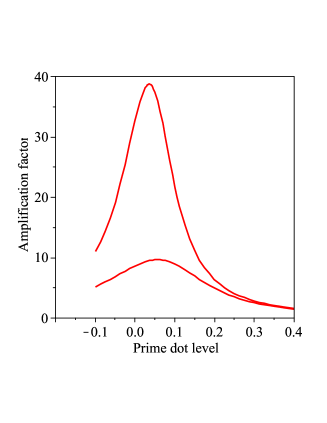
The amplification reaches its maximum when the difference comes up with , therefore the smaller , the bigger is the enhancement factor . The factor in the square brackets in Eq. (IV.1) behaves as in the vicinity of the band edge and thus gives additional contribution to this enhancement. Both analytical and numerical estimates confirm this statement. Experimentally, this effect should be observed as an increase of tunneling conductance on the boundary of Coulomb diamond in the vicinity of the threshold value of . A similar effect should arise on the hole side of the Coulomb diamond diagram (), where the occupied level crosses the top of the down spin valence band (solid lines in Fig. 3).
IV.2 Tunneling through moving dot
As is shown above, the canonical transformation allows one to distinguish between the adiabatic and non-adiabatic contributions to the tunneling amplitude. Let us first discuss the adiabatic corrections to the inelastic current given by Eq. (37) and illustrated by Fig. 4. In the vicinity in the point of the Coulomb diamond diagram the adiabatic position of the down spin level given by the solution of equation
| (41) |
rocks around or (see Fig. 2). This solution depends parametrically on time via the oscillating tunnel coupling . The above analysis of the static case prompts that time-dependent corrections become significant at finite bias close to the threshold value . The adiabatic evolution of the level in time near is given by the same Eq. (40), where the tunneling rate parametrically depends on . If the time-dependent perturbation is weak in comparison with the static value of tunneling rate, the temporal component of may be found perturbatively. Representing the tunneling rate as and expanding Eq. (40) around the time-independent value marked by index ’0’, we get
| (42) |
When deriving Eq. (42), the equality is used.
This time dependence turns into the corresponding adiabatic time dependence of tunnel conductance, mainly via the enhancement factor (39). One may expect that the slow adiabatic variations of will be especially distinct at corresponding to steep slopes of (Fig. 4) at near the boundary of the Coulomb diamond diagram (Fig. 3).
IV.3 Weak time dependent perturbation
Calculation accounting for nonadiabatic corrections to tunnel conductance is generally an extremely complicated nonlinear problem. To make it tractable, we assume that the time dependent part of is only a small periodic perturbation with respect to the time independent part and consider only the linear response given by the first harmonics. The nonlinear effects will be discussed separately. This approach allows one to pick out first nonadiabatic corrections to tunneling amplitude , which turns out to be small everywhere except in the vicinity of band edges.
Let us assume that the tunneling integral has the form
| (43) |
(here and below indices are omitted for the sake of brevity). Here . The solution of Eq. (III.2) is looked for in the form
| (44) |
where the time dependent corrections to are also small. Then we vary all the coefficients in Eq. (31) with respect to [see Eq. (11)] and and collect separately all the terms containing and respectively. Substituting then in (III.1), we reduce the scattering amplitude to the following form
| (45) |
where the coefficients of the cosine and sine terms can be explicitly calculated. The cosine coefficient
| (46) |
is obtained by varying equation (III.1) over the hybridization potential , whereas the sine coefficient
| (47) |
is obtained by varying equation (III.1) over the transformation parameter . After the variation in the form Eq. (11) can be substituted. Then
with
The most divergent terms in (46) and (IV.3) appear when we vary only explicitly written in Eq. (III.1) and in Eq. (III.1). As a result keeping the leading terms we have
| (48) |
and
| (49) |
The corresponding corrections to the tunneling transparency near the conductance band edge behave as
| (50) |
and
| (51) |
where
is the adiabatic correction to the tunneling rate for and the correction due to weak non-adiabatic effect for . Equation (IV.3) uses the fact that
for when . We use here the approximation similarly to the one used in Eq. (IV.1).
The term with the sine in equation (45) causes a phase shift between the oscillations of the hybridization parameter and the resulting current through the dot. If we neglect the dependence of the coefficients (46) and (IV.3) this phase shift can be readily found
It is expected to be generally rather small due to the factor , which is usually very small unless the dot level approaches the band edge . However close to the edge this factor diverges and results in an increasing phase shift,
As result the phase shift may become essential at .
The non-adiabatic corrections to tunneling conductance acquire the simple form of phase shift in oscillating cosine function only until the parameter is small and the perturbative approach is valid. With increasing one may expect appearance of higher harmonics in oscillating conductance. With further increase of the amplitude the language of quasi-energy levelsZ73 is more appropriate. We plan to discuss it elsewhere.
V Concluding remarks
We have discussed in this paper a new approach to the Anderson model for a half-metallic electron liquid in a tunnel contact with a moving nano-shuttle under strong Coulomb blockade. It is shown that in the situation where the spin-flip cotunneling processes are suppressed at low energies, the exact canonical transformation eliminating the tunneling term in the Anderson Hamiltonian exists even in the presence of strong Hubbard repulsion in the shuttle and time-dependent lead-shuttle tunneling. This canonical transformation in principle allows one to sort out the slow adiabatic renormalization of the energy levels and the tunnel transparency and to consider non-adiabatic corrections at least perturbatively. One may also include the inelastic spin-flip processes in the canonical transformation in the 4-th order of perturbation theory in , but these weak corrections do not change the above qualitative picture. We also have calculated the weak non-adiabatic corrections to tunneling transparency in a specific model of periodic sinusoidal motion of the shuttle. Undoubtedly, strong non-adiabatic effects should be taken into account in a more refined scheme: in the case of a periodic time-dependent perturbation one should appeal to the Floquet theorem in the time domain and use the quasi energy language.Z73 ; Baron77
Because of the energy gap for spin-flip processes in the half-metallic leads the Kondo cotunneling processes are suppressed, and the zero-bias anomaly in the tunnel conductance is absent. Physical manifestations of the shuttling mechanism under discussion arise in the form of time-dependent enhancement of conductance at finite bias near the boundaries of Coulomb diamonds on the phase diagram . The boundaries themselves are distorted due to the complete spin polarization of carriers (see Fig. 3), and even the Coulomb blockade step corresponding to occupation change from odd to even number of electrons in the dot is absent at zero bias. One may expect appearance of quasi energy satellites in this part of the phase diagram when the shuttle motion is essentially non-adiabatic. This regime is a subject for future studies.
Appendix A Time dependent canonical transformation
To diagonalize the Schrödinger equation (26) for the wave function , we conjecture the form
for the canonically transformed Hamiltonian. Then substituting and into Eq. (26), we obtain
| (52) |
The time derivative of exponent is found by means of the operator equation
| (53) |
Then using (53) and (25) in (52) yields
from where we straightforwardly get and Eq. (27).
Appendix B Tunneling amplitude for weak periodic potential
To derive the first non-vanishing time-dependent corrections to tunneling procedure, we vary the terms in Eq. (31). This variation procedure results in the two linear equations
| (54) |
where is explicitly real as defined in Eq. (11).
The first of these equations contains only explicitly imaginary terms whereas the second one contains only real terms. Therefore we have only two equation for four real variables (two complex variables). It is readily verified that
| (55) |
is a particular solution of the set of equations (54). One can also see that in the limit this solution reduces to the adiabatic approximation where we can take the results obtained in Subsection III.1 for the time independent problem and substitute there the tunneling amplitude (43) slowly varying in time.
The general solution of the corresponding homogenous set of equations reads
| (56) |
It should be added to the particular solution (55). The parameters and are meanwhile arbitrary. These parameters determined from the original cancelation equations (III.2) - (III.2) turn out to me small, and may result at most in nonadiabatic corrections .
In order to calculate the tunnel current we need the scattering matrix element
| (57) |
where the first term is obtained by substituting the solution (44), (55) into Eq. (III.1) and keeping the terms linear in . This contribution remains finite in the adiabatic limit . However it contains also nonadiabatic corrections due to the third term in (44). These corrections are determined by the equation
| (58) | |||
which contains derivatives and, hence, is purely nonadiabatic, i.e. disappears in the limit . Keeping only terms linear in in the scattering matrix element (57), we come to Eq. (45).
References
- (1) L.I. Glazman and M. Pustilnik in Nanophysics: Coherence and Transport, eds. H. Bouchiat et al (Elsevier, 2005), p. 427
- (2) R. Hanson, L.P. Kouwenhoven, J.R. Petta, S. Tarucha, and L.M.K. Vandersypen, Rev. Mod. Phys., 79, 1217 (2007)
- (3) H. Park, A. Lim, E. Anderson, A. Alevisatos, and P. McEuen, Nature 407, 57 (2000)
- (4) L.H. Yu and D. Natelson, Nano Letters 4, 79 (2004)
- (5) N. Roch, S. Florens, V. Bouchiat, W. Wernsdorfer, and F. Balestro, Nature 453, 634 (2008)
- (6) M. Bode, O. Pietzsch, A. Kubetzka, and P. Wiesendanger, Phys. Rev. Lett. 92, 067201 (2004)
- (7) C.F. Hirjibehedin, C.-Y. Lin, A.F. Otte, M. Ternes, C.P. Lutz, B.A. Jones, A.J. Heinrich, Science 317, 1199 (2007)
- (8) Y. Goldin and Y. Avishai, Phys. Rev. Lett. 81, 4688 (1998)
- (9) A. Kaminski, Yu. V. Nazarov and L.I. Glazman, Phys. Rev. B 62, 8154 (2000).
- (10) M.N. Kiselev, K. Kikoin, Y. Avishai, and J. Richert, Phys. Rev. B 74, 115306 (2006)
- (11) L.Y. Gorelik, R. Shekhter et al, Phys. Rev. Lett. 80, 4526 (1998)
- (12) D.V. Scheible and R.H. Blick, Appl. Phys. Lett. 84, 4632 (2004)
- (13) D.R. Koenig, E.M. Weig, and J.P. Kotthaus, Nature Nanotechnology, 3, 482 (2008)
- (14) K.A. Al-Hassanieh et al, Phys. Rev. Lett. 95, 256807 (2005)
- (15) L.I. Glazman, M.E. Raikh,Pis’ma Zh. Eksp. Teor. Fiz. 67, 1276 (1988) [JETP Lett. 47, 452 (1988)]
- (16) T.K. Ng, P.A. Lee, Phys. Rev. Lett. 61, 1768 (1988).
- (17) M.N. Kiselev, K. Kikoin, R.I. Shekhter, and V.M. Vinokur. Phys. Rev. B 74, 233403 (2006).
- (18) A. Goker, Solid State Commun. 148, 230 (2008)
- (19) R. López, R. Aguado, and G. Platero, Phys. Rev. Lett. 89, 136802 (2002)
- (20) J. Martinek, Y. Utsumi, H. Imamura, J. Barnaś, S. Maekawa, J. König, and G. Schön, Phys. Rev. Lett. 91, 17103 (2003)
- (21) B.R. Bułka and S. Lipiński, Phys. Rev. B 67, 024404 (2003)
- (22) M.-S. Choi, D. Sanchez, and R. Lopez, Phys. Rev. Lett. 92, 056601 (2004)
- (23) Y. Tanaka and N. Kawakami, J. Phys. Soc. Jpn, 73, 2795 (2004)
- (24) Y. Qi, J.-X. Zhu, S. Zhang, and C.S. Ting, Phys. Rev. B 78, 045305 (2008)
- (25) A.N. Pasupathy, R.C. Bialczak, J. Martinek. J.E. Grose, L.A.K. Donev, P.L. McEuen, and D.C. Ralph, Science 306, 86 (2004).
- (26) M.I. Katsnelson, V. Yu. Irkhin, L. Chioncel, A.I. Lichtenstein, and R.A. de Groot, Rev. Mod. Phys. 80, 315 (2008).
- (27) T. Jungwirth, J. Sinova, J. Masek, J. Kucera, and A.H. MacDonald, Rev. Mod. Phys. 78, 809 (2006).
- (28) K.A. Kikoin and V.N. Fleurov. Sov. Phys.–Zh. Eksp. Teor. Fiz. 77, 1062 (1979) [Sov. Phys. JETP 50, 535 (1979)].
- (29) K.A. Kikoin and V.N. Fleurov, Transition Metal Impurities in Semiconductors (World Scientific, Singapore, 1994).
- (30) M. Pustilnik, L.I. Glazman, J. Phys.: Cond. Mat. 16, R513 (2004)
- (31) F.D.M. Haldane and P.W. Anderson, Phys. Rev. B 13, 2553 (1976)
- (32) Y.B. Zeldovich, Uspekhi Fizicheskikh Nauk 110, 139 (1973) [Sov. Phys. Usp., 16, 427 (1973)]
- (33) S.R. Barone, M.A. Narowich, and F.J. Narowich, Phys. Rev. A 15, 1109 (1977)