Condensed Matter Theory Group, CPMOH, UMR 5798, Université Bordeaux I,33405 Talence, France
Electronic transport in mesoscopic systems Electronic transport in nanoscale materials and structures Electronic transport in interface structures
Spin-orbit effects in a graphene bipolar pn junction
Abstract
A graphene junction is studied theoretically in the presence of both intrinsic and Rashba spin-orbit couplings. We show that a crossover from perfect reflection to perfect transmission is achieved at normal incidence by tuning the perpendicular electric field. By further studying angular dependent transmission, we demonstrate that perfect reflection at normal incidence can be clearly distinguished from trivial band gap effects. We also investigate how spin-orbit effects modify the conductance and the Fano factor associated with a potential step in both and cases.
pacs:
73.23-bpacs:
76.63.-bpacs:
73.40.-c1 Introduction
There has been recent interest in a novel class of band insulators, called topological insulators (TIs) [1]. TIs are characterized by a bulk gap and a pair of time-reversed edge states at the boundary. These gapless edge states originate from the lattice spin-orbit (SO) effect and are protected by time-reversal symmetry from moderate disorder and interaction. In their seminal paper [2], Kane and Mele demonstrated that a graphene monolayer may become a TI when the intrinsic SO coupling dominates over the extrinsic Rashba coupling. Then the graphene layer is characterized by a topological number [3] and has gapless edge states that disappear if the Rashba coupling becomes too large, or if Coulomb interactions exceed a certain threshold [4]. Therefore the existence of the topological phase in graphene depends crucially on the values of the intrinsic and extrinsic (Rashba) SO couplings. In the concluding section, we shall discuss recent estimates of these SO interactions which allows for considering the transition between the topological () and ordinary () phases.
Since the insulating regime is rather difficult to access experimentally, we propose to characterize this crossover by transport properties in the doped regime. In particular we stress that transport through a bipolar junction should differ in the distinct cases and respectively. Quasi-relativistic Klein tunneling [5] was demonstrated experimentally [6, 7, 8, 9, 10, 11, 12] by using local gating techniques, and the corresponding theory have received a great deal of attention [13, 14, 15, 16] in the absence of SO coupling ().
In this Letter, we obtain the angular dependent transmission of a junction in the presence of both intrinsic and Rashba SO couplings. At normal incidence, we show that the junction transmission exhibits a crossover from perfect reflection to perfect transmission when the Rashba coupling is tuned by the perpendicular electric field. We also predict the conductance and the Fano factor associated with a potential step in presence of intrinsic and Rashba SO couplings.
Similar topological phases have also been predicted [17] and now observed [18] in materials with larger SO interactions such as HgTe/CdTe quantum wells. The protected edge states appear when the width of the HgTe layer exceeds a critical value. We choose to study graphene since the Kane-Mele is the simplest possible model that have four spin-split bands, which is the minimum required for the nontrivial phase to exist [19, 20]. Moreover our predictions might be compared to the studies of Klein tunneling in graphene performed in the absence of SO coupling ().
2 Kane-Mele model and single valley approximation
The Kane-Mele model describes the low-energy dynamics of quasiparticles near the and points of graphene in the presence of spin-orbit effects [2]. The corresponding Hamiltonian acts on the slowly varying envelop of electronic Bloch wavefunctions, which are indexed by real spin (Pauli matrices , ), lattice isospin () and valley isospin () quantum numbers. The kinetic Hamiltonian
| (1) |
describes massless Dirac fermions and is spin-independent. In the following we shall use units with .
The intrinsic spin-orbit effect is completely determined by the symmetries of the honeycomb lattice and by the geometry of the carbon orbitals. It can be described by the Hamiltonian
| (2) |
where is the value of the gap induced at (and ). This form can be deduced from group theoretical techniques [2] or as the low-energy limit of tight-binding models [21, 22, 23]. It was shown recently that can be increased by inducing a curvature of the graphene layer [22].
In the presence of a perpendicular electric field (generated by the distant gate), there is an additional Rashba spin-orbit coupling [24]
| (3) |
where is proportional to the electric field.
In the following we shall restrict ourselves to transport through potential barriers which are smooth on the scale of the atomic lattice period. Therefore we shall neglect intervalley scattering by using a single-valley version of the Kane-Mele Hamiltonian wherein the eigenvalue of is replaced by (or ) for (or ). The resulting Hamiltonian consists in a matrix applying to spinors of the form , where t represents transpose. Here the arrow index (, ) stands for real spin while the index () denotes the two inequivalent sites of the honeycomb lattice.
3 Band structure
In the homogeneous case, the two-dimensional momentum is a good quantum number. The single valley Kane-Mele Hamiltonian is diagonalized by the eigenspinors as
| (4) |
where are band indices. The four energy bands are characterized by the dispersion
| (5) |
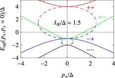
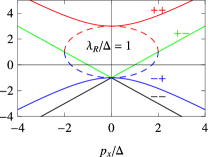
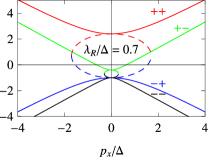
where . The energy spectra has distinct features depending on the value of the ratio (Fig. 1).
In the absence of Rashba coupling, the intrinsic spin-orbit coupling opens a gap at separating the conduction band from the valence band , each one still having a two-fold degeneracy with respect to .
A finite Rashba interaction generates a splitting of those bands which may eventually close the gap. In that sense the intrinsic and Rashba SO effects compete each other. When the intrinsic SO dominates (), the system is a band insulator whereas it is a gapless semimetal with quadratically dispersing bands in the opposite case (). The intermediate case is rather special since two linearly dispersing bands are recovered. Nevertheless the system differs from the graphene spectrum in the absence of SO coupling by the presence of two additional spin-split parabolic bands .
In coordinate representation, the eigenspinors are plane waves with
| (6) |
and . The normalization factor is simply
Note that for a given energy , the band index is automatically determined. The spinor Eq. (6) also describes evanescent modes characterized by a purely imaginary (superposed in broken curves in Fig. 1). Naturally, those modes cannot exist in an infinite sheet, but they develop in the presence of an interface (see below the interface between the and doped regions) and contribute to the scattering properties.
Eigenstates with different momentum or energy are obviously orthogonal to each other . Here we amphasize that the eigenstates Eq. (6) of the Kane-Mele model satisfy an additional orthogonality relation: when . Moreover the band indices and play very different roles: index determines the symmetry of wave function, while specifies whether the state belongs to the conduction or the valence band. In Fig. 1 (b), two energy bands with the same band index combine to form a linear Dirac spectrum. The orthogonality between eigenstates with different also holds true for evanescent modes realized in the vicinity of -junction.
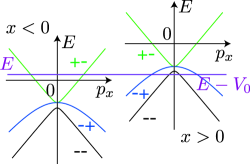
4 The -junction Model
We now introduce our model of a -junction in a monolayer of graphene described within the Kane-Mele model. We assume that an electrostatic gate creates a potential barrier which is smooth on the scale of the atomic lattice. Moreover we consider an idealy pure system, a situation which have been approached experimentally in suspended devices [25, 26]. Then no inter-valley scattering is involved, i.e. and points are decoupled. One can use safely the single-valley approximation and describe the junction by the -band Hamiltonian
| (7) |
where the term is diagonal in both spin and lattice isospin degrees of freedom. Moreover we assume that the barrier is sharp on the scale of the Fermi wavelength in each of the metallic bands at right and left. In this sense, we shall investigate the scattering by an abrupt barrier defined by
| (8) |
Note that we also assume a straight interface with translational invariance along the direction (no roughness along the interface ).
5 Scattering states
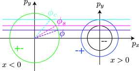
We investigate how incident fermions from the left are scattered by the potential barrier . The left side () being always in the doped metallic regime, transport across the junction is dominated by extended two-dimensional waves while helical edge states are irrelevant here. Owing to translational invariance along the axis, the momentum is a good quantum number and factors can be omitted accordingly. We now construct scattering states at the Fermi level defined by their energy and momentum . We choose the energy such that incident particles are injected from the single band , which is realized for .
The scattering state on the incident side takes the following form:
| (9) |
where , , and . The wavevectors of the incident, reflected and evanescent waves are respectively and , with
| (10) | |||||
| (11) |
On the transmitted side, the wavefunction reads
| (12) |
where and are amplitude and wavevector of the two transmitted waves . The spinors and represent either a propagating or an evanescent ( becomes pure imaginary) mode depending on the sign of
| (13) |
If , the mode in the corresponding band is propagating. The actual sign of is chosen such that the group velocity is positive, thereby describing an outgoing transmitted wave packet. In the specific case of inter-band tunneling, the positive group velocity is realized by a negative momentum state ( in Eq. (5)) implying . If , the mode in the corresponding band is evanescent.
Demanding continuity of the wavefunctions at the interface:
| (14) |
we obtain four independent scalar equations for the scattering parameters : , , and . Thus the reflection probability is determined uniquely from Eq. (14) for given , and .
6 Transmission at normal incidence
We examine here the normal incidence transmission () through the junction in the presence of Rashba and intrinsic SO effects. The junction is defined by Eq. (8) together with the condition to insure inter-band tunneling.
6.1 Decoupling at normal incidence
When , the continuity equation Eq. (14) reduces to two decoupled equations
| (15) | |||||
| (16) |
due to the symmetry of the spinors. Indeed, the full Hilbert space is the direct sum of two orthogonal subspaces. The spinors and belong to the subspace spanned by and , where t represents transpose. The spinors and belong to the orthogonal subspace spanned by and .
6.2 Dominant Rashba effect
At large enough Rashba coupling, namely there is one propagating () and one evanescent () transmitted waves, momenta and being respectively real and purely imaginary. As a result, Eq.(17) yields unimodular reflection amplitude , thereby indicating perfect reflection. This nontrivial total reflection arises because the only propagating transmitted wave () is orthogonal to the incident wave () at normal incidence. This situation is similar to inter-band tunneling in bilayer graphene as we shall discuss later. For smaller Rashba coupling both transmitted waves are propagating leading to finite transmission through the wave. Accordingly the momentum is real and Eq.(17) implies partial reflection, i.e. .

6.3 Balanced Rashba and intrinsic SO effects
At , the bands become linear and combine to form a Dirac cone. Meanwhile, the spinors show further orthogonality relations in addition to the one with respect to . Namely, at this particular value the reflected wave becomes orthogonal to the incident wave, thereby implying perfect transmission. In the case of (mono-layer) graphene in the absence of SO effects, the total absence of backscattering at normal incidence is due to the chiral symmetry, i.e. (: time-reversal operator), and Berry phase [27, 13]. Another important consequence of chiral symmetry is the anti-localization in the absence of inter-valley scattering [29]. Here, in the Kane-Mele model, and the Berry phase is , due to the activation [30] of real spin by Rashba SO coupling. As a result the system shows standard weak localization in the absence of inter-valley scattering [30].
6.4 Topological gap phase
At large intrinsic SO coupling , both and describe propagating waves. Therefore the reflection is only partial.
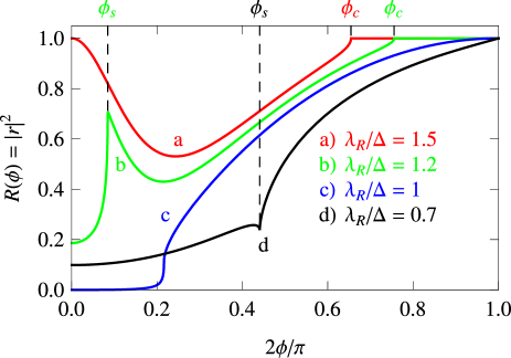
Summarizing this section, we have seen that the junction shows a crossover from perfect reflection at large Rashba coupling towards perfect transmission when , while finite reflection is restored at smaller values of the Rashba coupling (Fig. 2). These contrasted behaviors are reminiscent of those of a junction in single and bilayer graphene which show respectively perfect transmission and perfect reflection at normal incidence [13, 28]. These remarkable features originate from the orthogonality between the incident and scattered spinors at normal incidence. However, this orthogonality relation between and is broken as soon as becomes finite.
It is worthy to note that the parameter in the Kane-Mele model plays formally the role of inter-layer hopping in bilayer graphene. Thus monolayer graphene with only Rashba SO has the same structure as that of spinless bilayer graphene, and shows the same charge transport properties.
7 Transmission at arbitrary incidence
We now focus on the angular dependence of the transmission through a bipolar junction. The reflection probability is obtained by solving the continuity equation Eq.(14), the incident angle satisfying .
7.1 Dominant Rashba effect (
As discussed previously the junction exhibits a perfect reflection at normal incidence for large enough Rashba coupling . As one varies the incident angle from normal incidence (), the reflection coefficient decreases and the curve exhibits a broad dip (curve , Fig. 3.a). This feature clearly distinguishes the perfect reflection due to orthogonality in the normal incidence from the perfect reflection due to a band gap on the transmitted side. In the case of perfect reflection due to band gap, the reflection probability remains trivially equal to unity when one varies the incident angle away from normal incidence. At large incidence , one recovers total reflection. The critical angle is determined by a condition on the Fermi wavevectors in the bands and as shown in Fig. 4.
For intermediate Rashba coupling , reflection is only partial at and the curve exhibits a peak (curve , Fig. 3.b). The initial increase of from to is related to the overlap between the incident wave and transmitted ( and ) waves. At small incidence, the dominant effect is the reduction of the overlap with the mode yielding an increasing reflection probability. The local maximum of at appears when the mode turns to evanescent (Fig. 4, upper panel). For slightly larger incidence , the dominant effect is the increase of the overlap between the incident wave and the (propagating) transmitted mode, thereby providing a decrease of . Above the critical angle , both transmitted modes become evanescent at , thereby leading to (Fig. 4).
7.2 Balanced case
When , the property of perfect transmission (which is exact at ) pertains quite accurately to a broad range around normal incidence (curve , Fig. 3.c).
7.3 Topological gap phase
When , the reflection probability shows a sharp dip (curve , Fig. 3.d) at the angle where mode turns to evanescent (Fig. 4, upper panel). The nature of this singularity is similar to that of peak structure at intermediate Rashba coupling already discussed. The singularity appears when , which means for . Note that and bands are symmetric w.r.t. .
8 Conductance and shot noise
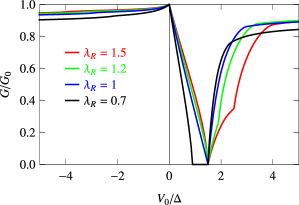
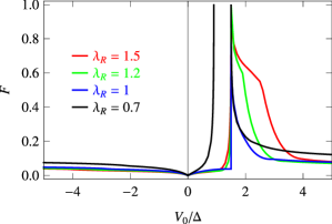
The conductance and the Fano factor associated with the potential step are readily obtained from the transmission probability, as described in [13, 14, 15, 16]. In the balanced case , the conductance curves (Fig. 5, left panel) do not differ significantly from the case of no SO effects () [15, 16]. In contrast, the vanishing of the conductance within a finite range of reveals that graphene is gapped when intrinsic SO dominates Rashba coupling. The Fano factor is, on the other hand, not well-defined in the gap. The Rashba dominated regime also exhibits anomalous features: a cusp in and an enhancement of the Fano factor. The peak in is rather asymmetric with a characteristic shoulder that broadens when increasing the Rashba coupling (Fig. 5, ).
The corresponding experiments should be done on graphene with very low absolute Fermi energies on both sides of the junction. Therefore disorder may hinder the observation of the crossover from perfect reflection to perfect transmission at the -junction [32]. Nevertheless on-going progress in sample preparation might eventually render the spin-orbit effects observable in suspended graphene devices [25, 26]. The SO interaction is commonly supposed to be weak owing to the low atomic number of carbon. Nevertheless, first estimates indicated the favorable conditions for the TI to exist, namely a sizeable spin-orbit gap K at the points and a tiny Rashba splitting mK for a typical electric field V/ nm [2]. Unfortunately due to the specific geometry of and orbitals in graphene, the actual intrinsic SO coupling should be far smaller, namely mK, while the Rashba splitting is enhanced to typical values mK for V/ nm [21, 22, 23]. Recently, first-principle calculations suggested that orbitals might play a dominant role in the gap opening at and points [31]. As a result, the spin couplings are predicted to assume intermediate values ( K) between the estimates of [2] and of [21, 22, 23]. Such close values and the possibility to tune both Rashba and intrinsic SO couplings allows to consider the transition between the topological () and ordinary () phases.
9 Concluding remarks
We have shown that at normal incidence the junction transmission exhibits a crossover from perfect reflection at large Rashba coupling to perfect transmission when the Rashba coupling exactly balances the intrinsic spin orbit coupling. Further study on the angular dependence enabled us to clearly distinguish such unique features from trivial band gap effects. Finally we have obtained the conductance and the shot noise associated with an electrostatic potential step realized in a graphene monolayer with competing spin-orbit effects.
Acknowledgements.
A.Yamakage and K.I. Imura are supported by KAKENHI (A.Yamakage: No. 08J56061 of MEXT, Japan, K.I. Imura: Grant-in-Aid for Young Scientists B-19740189). J. Cayssol acknowledges gratefully support from the Institut de Physique Fondamentale (IPF) in Bordeaux.References
- [1] M. König, H. Buhmann, L.W. Molenkamp, T.L. Hughes, C.X Liu, X.L Qi and S.C Zhang, J. Phys. Soc. Jpn 77, 031007 (2008).
- [2] C.L. Kane and E.J. Mele, Phys. Rev. Lett. 95, 226801 (2005).
- [3] C.L. Kane and E.J. Mele, Phys. Rev. Lett. 95, 146802 (2005).
- [4] C. Wu, B.A. Bernevig and S.-C. Zhang, Phys. Rev. Lett. 96, 106401 (2006).
- [5] O. Klein, Z. Phys. 53, 157 (1929).
- [6] B. Huard et al., Phys. Rev. Lett. 98, 236803 (2007).
- [7] J.R. Williams, L. DiCarlo, and C.M. Marcus, Science 317, 638 (2007).
- [8] B. Ozyilmaz et al., Phys. Rev. Lett. 99, 166804 (2007).
- [9] J.B. Oostinga et al., Nature Mat. 7, 151 (2008).
- [10] R. V. Gorbachev et al., Nano Lett. 8, 1995 (2008).
- [11] N. Stander, B. Huard, and D. Goldhaber-Gordon, Phys. Rev. Lett. 102, 026807 (2009).
- [12] G. Liu et al., Appl. Phys. Lett. 92, 203103 (2008).
- [13] M.I. Katsnelson, K.S. Novoselov, and A.K. Geim, Nature Phys. 2, 620 (2006).
- [14] V.V. Cheianov, V.I. Falko, Phys. Rev. B 74, 041403(R) (2006).
- [15] J. Cayssol, B. Huard, and D. Goldhaber-Gordon, Phys. Rev. B 79, 075428 (2009).
- [16] E.B. Sonin, Phys. Rev. B 79, 195438 (2009).
- [17] B. A. Bernevig, T. L. Hughes, and S.C. Zhang. Science 314, 1757 (2006).
- [18] M. König, S. Wiedmann, C. Brüne, A. Roth, H. Buhmann, L. Molenkamp, X.-L. Qi, and S.C. Zhang, Science 318, 766 (2007).
- [19] S. Murakami et al., PRB 76, 205304 (2007).
- [20] X-L. Qi et al., PRB 78, 195424 (2008).
- [21] H. Min, J.E. Hill, N.A. Sinitsyn, B.R. Sahu, L. Kleinman, and A.H. MacDonald, Phys. Rev. B 74, 165310 (2006).
- [22] D. Huertas-Hernando, F. Guinea, and A. Brataas, Phys. Rev. B 74, 155426 (2006).
- [23] Y. Yao, F. Yei, X.L Qi, S.C. Zhang, and Z. Fang, Phys. Rev. B 75, 041401(R) (2007).
- [24] Y.A. Bychkov and E.I. Rashba, JETP. Lett. 39, 78 (1984).
- [25] X. Du et al., Nature Nanotechnology 3, 491 - 495 (2008).
- [26] K. I. Bolotin et al., Phys. Rev. Lett. 101, 096802 (2008).
- [27] T. Ando, T. Nakanishi and R. Saito, JPSJ 67, 2857 (1998).
- [28] A. H. Castro Neto, F. Guinea, N. M. Peres, K. S. Novoselov, and A. K. Geim, Rev. Mod. Phys. 81, 109 (2009).
- [29] H. Suzuura, T. Ando, Phys. Rev. Lett. 89, 266603 (2002).
- [30] K. I. Imura, Y. Kuramoto and K. Nomura, Phys. Rev. B 80, 085119 (2009)
- [31] M. Gmitra, S. Konschuh, C. Ertler, C. Ambrosch-Draxl, and J. Fabian, arXiv:0904.3315.
- [32] J. Martin et al., Nature Physics 4, 144 - 148 (2008).