Electronic and hole minibands in quantum wire arrays of different crystallographic structure
Abstract
We consider quantum wire arrays consisting of GaAs rods embedded in AlxGa1-xAs and disposed in sites of a square or triangular lattice. The electronic and hole spectra around the conduction band bottom and the valence band top are examined versus geometry of the lattice formed by the rods, concentration of Al in the matrix material, and structural parameters including the filling fraction and the lattice constant. Our calculations use the envelope function and are based on the effective-mass approximation. We show that the electronic and hole spectra resulting from the periodicity of the heterostructure, depend on the factors considered and that the effect of lattice geometry varies substantially with lattice constant. For low lattice constant values the minigaps are significantly wider in the case of triangular lattice, while for high lattice constant values wider minigaps occur in the square lattice-based arrays. We analyse the consequences of our findings for the efficiency of solar cells based on quantum wire arrays.
pacs:
84.60.Jt, 73.21.Cd,17.40.+wI Introduction
Semiconductor periodic heterostructures have an additional, superstructure-related discrete translational symmetry, the period of which is much larger than that of the atomic lattice. This causes electronic and hole minibands, with minigaps between them, to form near the bottom of the conduction band and the top of the valence band, respectively, in the electronic/hole spectrum of the structure. In superlattices, heterostructures periodic in a one dimension (1D), the electronic/hole band splits at the boundary and in the centre of the first Brillouin zone to form minibands separated by minigaps of width equal to the difference between the conduction band bottom or the valence band top, respectively, in the component materials of the superlattice.davison92 Similar effects occur also in quantum wire arrays, semiconductor heterostructures periodic in two dimensions (2D), but the opening of minigaps and their width, determined in a more complex way by factors which include structural parameters in addition to material parameters, can only be studied numerically. The effects in question are also observed in other periodic composites, such as photonic, phononic or magnonic crystals, in the dispersion of electromagnetic, elastic or spin waves.yablonovitch87 ; john87 ; siglas93 ; vasseur94 ; vasseur08 ; vasseur96 ; krawczyk08 ; tkachenko09
Aroused many years ago and persisting ever since, the interest in periodic semiconductor heterostructures stems from the possibility of fabricating systems with the conduction or valence band split into a desired pattern of discrete minibands and minigapsbryant89 ; nika07 ; gershoni93 ; this could be achieved through systems of semiconductor dots or rods of properly designed size and shape (cylinders, cubes, prisms, rings or antirings)cusack96 ; tkach02 ; planelles06 ; planelles07 . The discrete spectra of electronic conduction or valence bands significantly modify the electron or hole transport as well as the optical properties of the structure. Used in photovoltaic and thermoelectric cells, semiconductor heterostructures allow construction of devices converting lightbarnham97 ; green03 ; nozik02 ; jiang06 ; shao07 or temperature differencebalandin03 ; lin03 ; yang04 ; broido06 into electric current with efficiency higher than that allowed by homogeneous materials. Although the two effects differ in nature, the electronic or hole band structure plays an important role in both. The numerous theoretical studies on the subject use various approximations and methodsallmen92 ; harrison05 ; mingo07 ; gomez02 ; lazrenkova01 ; broido06 ; duque99 of determining the energy spectrum of 2D and 3D heterostructures. Here we use the plane wave method with the effective-mass approximation, a technique successfully applied to studying the electronic states in 1D, 2D and 3D heterostructures with quantum dots and wires of different shape and size, as well as interdiffusion and strain effects on electronic bands.cusack96 ; gershoni88 ; li98 ; li05 ; tkach00 ; ngo06
The main objective of this study is to investigate the effect of the crystallographic structure on the electronic/hole spectrum in quantum wire arrays. In particular, we are going to determine the conditions conducive to the opening of minigaps in the conduction band and in the valence band. Besides its purely scientific aspect, our investigation is of practical importance for photovoltaic cells, the efficiency of which is determined by the electronic structure of the active material in which the photoelectric effect takes place. If the active material is a periodic semiconductor heterostructure, the efficiency of the cell will substantially depend on the width of the electronic energy minigap between the lowest miniband and the rest of the conduction band.klos09
The paper is organized as follows. In Section II we present in detail the plane wave method applied to the equation for the electronic envelope function in quantum wire arrays, and discuss the approximations used. Section III discusses the results of our calculations obtained for the conduction band in a quantum wire array consisting of GaAs rods embedded in AlGaAs and forming a square or triangular lattice. The spectra of these 2D heterostructures are studied versus Al concentration in the matrix material, filling fraction and lattice constant. In Section IV we analyse the energy spectrum of the valence band in the same heterostructures. The paper is summed up in Conclusions, in which we indicate the implications of our results for the efficiency of solar cells based on quantum wire arrays.
II Plane wave method in effective-mass approximation
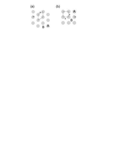
Let us consider a quantum wire arrays consisting of infinitely long rods of material A forming a square or triangular lattice and embedded in a matrix of material B (Fig. 1). The rod axes are oriented along the direction. The rods are assumed to represent potential wells for propagating electrons and holes.
Here we shall only consider arrays with rods of circular cross section. The effect of the cross-sectional geometry of the rods has already been studied in our earlier paper klos09 , in which we established that the efficiency of solar energy conversion in the photoelectric effect only slightly depends on the shape of the rods and that their circular cross section is optimum in this aspect. The filling fraction , defined as the area ratio of the rod cross section to the unit cell of the heterostructure, will be a measure of the rod size. The maximum filling fraction value corresponds to the situation in which rods touch the unit cell limits. For a square or triangular lattice of cylindrical rods with cross-section radius the filling fraction can be calculated from the following respective formulae:
| (1) |
where is the distance between adjacent lattice sites.
Our calculations of the electronic band structure of 2D semiconductor heterostructures will be performed in the effective-mass approximationbustart88 ; burt99 ; califano00 , which means that we shall restrict our attention to the bottom (and top) of the parabolic conduction (and parabolic valence) band in the electronic (hole) spectrum of the constituent semiconductors. Such approximations prove to be very useful in the electronic band calculations for semiconductor heterostructures with various component materials, as well as for single dots.califano00 ; harrison05 ; tablero05 ; califano00b ; duque99 We shall assume the interactions between the single conduction band and the two valence bands are negligible; this allows independent determination of the electronic miniband structure in the conduction band (Sections II and III in the single band approximation) and the hole miniband structure in the valence band (Section IV).
Electronic states are described by the Ben-Daniel-Duke equation:duke
| (2) |
with effective mass (isotropic in a homogeneous medium) and effective potential determining the position of the conduction band bottom; denote the position vector in the plane of the periodicity; denotes the envelope wave function of conduction band electrons. The constant (where and denote the free electron mass and charge, respectively) allows to express the energy in electronvolts (eV) and the coordinates , in angstroms Å. The material parameters: the effective mass and the effective potential, vary in space with the periodicity of the heterostructure:
| (3) |
where is a lattice vector ( in square and in triangular lattice, and being integers).
The expansion of the electron envelope function in the plane-wave basis and the Fourier expansion of the material parameters can be written as:
| (4) |
where are Fourier coefficients of the periodic factor of the envelope function (which has the same periodicity as the quantum wire arrays) and is a wave vector from the first Brillouin zone. Fourier coefficients of the material parameters, and , can be found analytically from the formula:
| (5) |
where and denote, respectively, the periodic material parameter (the effective mass or the effective potential) and the corresponding Fourier coefficient for a plane wave of wave vector equal to vector of the reciprocal lattice ( for square lattice, for triangular lattice, and being integers); denotes the area of the periodic heterostructure unit cell. The explicit form of the Fourier coefficients (5) for rods of circular cross section is:
| (8) |
where functions and are the values of potential ( and ) or effective mass inverse ( and ) in the cylinders and in the matrix, respectively, and is a Bessel function of the first kind.
The substitution of expansions (4) in the Schrödinger equation (2) leads to the following system of equations representing an eigenvalue problem, the solution of which yields Fourier coefficients of the periodic factor of the envelope function and the electron energy :dobrzynski95 ; cusack96
| (9) |
When a finite number of reciprocal lattice vectors is used in the Fourier series (4) also the system of equations (9) becomes finite. We have solved this system of equations by standard numerical procedures designed for solving symmetrical matrix eigenvalue problems, and tested the eigenvalues found for convergence, as necessary in procedures of this type. For all the structures considered in this study a satisfactory convergence of numerical solutions of Eq. (4) for first few bands proves to be attained with the use of 169 reciprocal lattice vectors.
III The effect of the crystallographic structure on the conduction band
The results presented in this Section have been obtained for rods of gallium arsenide (GaAs) embedded in a matrix of gallium arsenide doped with aluminium (AlxGa1-xAs, where is the concentration of Al ions). In this case the depth of the potential wells is determined by the concentration of Al in the matrix: growing matrix Al concentration will increase the effective potential in the matrix, and thus deepen the potential wells felt by conduction band electrons. We have used the following empirical formulae for a linear extrapolation of the material parameter values in GaAs and AlAs to estimate their values in the AlxGa1-xAs matrix: and .param ; param2
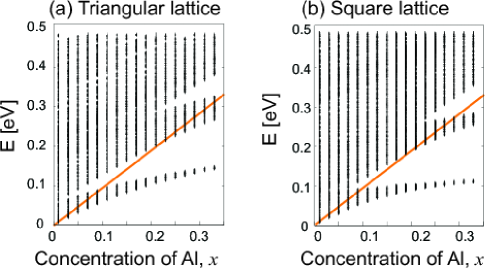
The effective-mass approximation is justified by the occurrence of a direct gap at point of the atomic band structure for low concentrations of Al in both the rods and the matrix. To meet this condition of approximation applicability, the Al concentration in the matrix was only allowed to range from 0 to 0.35. Also calculated in the envelope function approximation and by the plane wave method, the electronic band structure (the conduction band) of square lattice-based heterostructures presented in [bryant89, ; dobrzynski95, ; krawczyk09, ] is in agreement with the results obtained in this study from Eq. (9).
Figure 2 (a) and (b) shows the energy structure of conduction band electrons versus Al concentration in a 2D heterostructure with GaAs rods disposed in sites of a triangular or square lattice. The calculations were performed at fixed lattice constant = 120 Å and filling fraction . Increasing results in deepening potential wells, in which electrons from first minibands localise and the interaction between electrons in neighborhood wells weakens. As a consequence the miniband shrinks and increase their energy, and the minigap that separates it from the quasi-continuous conduction band above grows wider. There are also some differences between lattices: in the triangular lattice case the first miniband is seen to occur almost throughout the considered range of Al concentration (from up), while in the square lattice case the Al concentration must be above a critical value for the gap to open. Note from Al concentration up the first minigap is wider in the square lattice case than in the triangular lattice case. The second minigap (between the third and the fourth miniband) only opens at and , for the square and triangular lattice, respectively, and is wider in the square lattice-based structure.
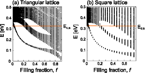
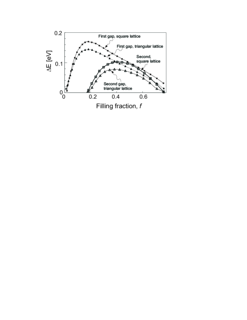
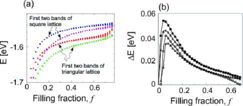
Let us see how the band structure varies with filling fraction. Figure 3 shows plots obtained for matrix Al concentration fixed at and for lattice constant Å in the triangular and square lattice case. As expected, the minibands are seen to shift down as the filling fraction grows due to widening of the wells and to become wider because of shrinking of matrix (barrier) materialkrawczyk09 . The filling fraction dependence in both structures is very similar in terms of ranges of minigap occurrence as well as filling fraction values corresponding to the maximum width of the first and second gap, and , respectively (see Fig. 4). Note, however, that in the case of rods forming a square lattice both the first minigap and the second one are wider, their respective widths being 0.17 eV and 0.1 eV, against 0.14 eV and 0.08 eV in the triangular lattice case. These small differences between electronic bands in square and triangular lattices in dependence on and can be explained as follows.
A major difference between a triangular lattice and a square lattice is the number of nearest neighbours; in a triangular lattice-based structure each well (rod) has 6 neighbours (at a distance ), against 4 neighbours (at a distance ) in the square lattice case. A larger number of nearest neighbours implies more interactions, if exist, and wider energy bands for the same parameter values, hence minibands in the triangular lattice case should be slightly wider than in a square lattice-based structure with the same values of , and (especially those with high energy, e. g. compare Figs 2 (a) and (b) or Figs 3(a) and (b)). Obviously, this affects the minigap width, in which differences are seen as well, Fig. 4. Let us get back to the definition of filling fraction, (1), to determine the radii of the cylindrical rods corresponding to equal filling fraction in both types of lattice at equal lattice constant values. The cylindrical rods are found to have larger diameter in the square lattice case (), which implies relatively lower energies of the lowest minibands associated with electrons in wells, and consequently, increased isolation of these states, and narrower bands, also conducive to wider minigaps. However, it should be kept in mind that the spacing between rods decreases as their diameter grows, which can lead to increased overlapping of the wave functions of adjacent rods, and consequently, to wider minibands. The impact of these two competing effects can be expected to depend on the lattice constant.
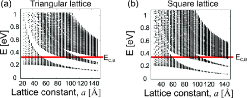
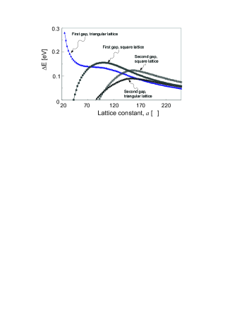
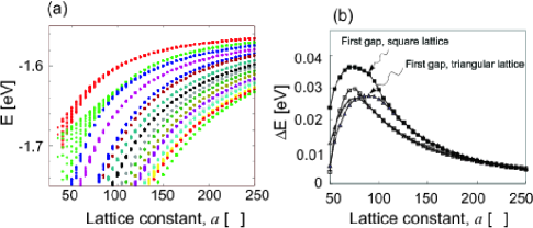
Let us compare plots depicting the band structure versus the lattice constant in the square and triangular lattice case (Fig. 5). In this dependence the electronic band structures in the two cases considered differ the most. In the triangular lattice case the first minigap is seen to occur throughout the considered lattice constant range, i.e. from 25 Å to 150 Å, while in the square lattice case the gap only opens above Å. For the second gap the critical lattice constant values are Å and 92 Å in the triangular and square lattice case, respectively. In Fig. 6 the width of minigaps in the square and triangular lattice-based heterostructures is represented by the respective shapes, i.e. squares and triangles. Filled and outlined symbols refer to the first and second gap, respectively. For low lattice constant values a single gap is seen to occur in the triangular lattice case; the width of this gap decreases monotonously with increasing lattice constant from 0.3 eV for Å to 0.06 eV for Å. In the square lattice case the width of the first gap is seen to vary with in a non-monotonous manner: from Å up the gap widens to reach a maximum width of 0.16 eV at lattice constant 100 Å, and then narrows down as increases still further. For Å the first gap has equal width in both cases. The second gap has a maximum width for Å for both lattice types considered, but tends to be wider in the square lattice case. Thus, for large lattice constant values we observe the relations already explained above.
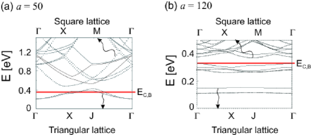
Let us try to elucidate the intriguing relations found in the range of low lattice constant values. Two effects occur as a result of reducing the lattice constant at fixed filling fraction: (a) the rod (potential well) diameter decreases, with a concurrent increase energy of bands; at the same time, (b) the distance between adjacent wells decreases, which implies increased overlapping of wave functions and thus steps up the widening of bands. But it doesn’t explain relations for Å where the top of the first miniband is already above the barrier, for both arrangements and electron waves can propagate across the structure slightly scattered by the barrier. It means, that triangular lattice, due to a larger number of adjacent wells, favors destructive interference of such waves resulting in wide gap, as opposed to square lattice, where the gap disappear. Figure 7 shows the band structures, calculated along the path and in the first Brillouin zone, of triangular (solid lines) and square (dashed line) lattice-based 2D heterostructure, respectively, with lattice constant Å (a) and Å (b). As expected the bands are seen to be very wide in the quantum wire arrays with low lattice constant value, Fig. 7 (a), and very narrow in the arrays with large lattice constant Fig. 7 (b). In Fig. 7 (a) we can observe additional difference in band structures for triangular and square lattices. For triangular lattice separating the first miniband form the second one at X point remains almost unaltered in comparison to point J. In the case of square lattice the separations both in X and M point are reduced as lattice constant decreases. This effect and some small shift of miniband position between points X and M cause the closing of absolute minigap in square lattice whereas for triangular lattice this minigap remains open.
IV The effect of the crystallographic structure on the valence band
For calculating the valence band structure of quantum wire arrays we use the plane wave method, applied to the Schrödinger equation of the envelope function of light and heavy hole states near the top of the valence band:datta08
| (10) |
where and are envelope functions for light and heavy holes, respectively, and operators , and have the form:
| (11) | |||||
Luttinger parameters , , , describing the effective masses and of light and heavy holes, respectively, near point of the atomic lattice, are, like the position of the valence band top , periodic in the heterostructure.
Expanded in the plane-wave basis by a procedure similar to that employed in the case of the conduction band, equation (10) can be written as a Hermitian eigenvalue problem for interacting light and heavy holes:
| (12) |
where and are expressed as follows:
| (13) | |||||
and have the sense of Fourier coefficients for periodic factors of the envelope functions of heavy and light holes, respectively, and ( = 1, 2 or 3) and are the respective Fourier coefficients of Luttinger parameters and , which can be found from (8) for the Luttinger parameter values, specified below, in the rod material A and in the matrix material B.
Again, let us consider a heterostructure consisting of a triangular or square lattice-based system of GaAs rods embedded in AlxGa1-xAs. The following material parameter values, dependent on the concentration of Al in aluminium gallium arsenide, can be assumed:param ; param2
| (14) |
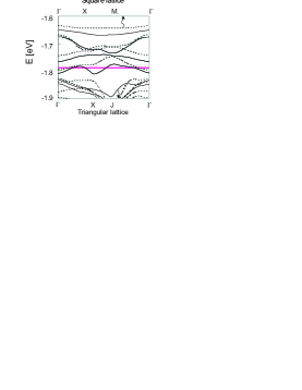
Fig. 8 shows the wave vector dependence of hole minibands plotted along the irreducible part of the first Brillouin zone in a triangular lattice-based heterostructure (solid line, path ) and in a square lattice-based heterostructure (dashed line, path ). The calculations were performed for lattice constant Å, filling fraction and matrix Al concentration .
Comparing the hole energy structure (Fig. 8) with the energy structure of conduction band electrons (Fig. 7), we notice the hole bands (for light and heavy holes) are much narrower and arranged very densely, so their role in photoelectric effect will be minor. The first three electronic bands lie in the energy range from 0.21 eV to 1.14 eV, against -1.76 eV to -1.65 eV in the case of hole bands (the negative energy values are a consequence of assuming the energy of a conduction band bottom electron as the zero energy level). The lattice type-related differences in energy structure will be better visualised in the dependence of hole minibands on the lattice constant and the filling fraction.
The lattice constant dependence of the band structure in the triangular lattice case is depicted in Fig. 9(a). The minibands are seen to shift towards higher energies and shrink as the lattice constant increases. A similar tendency is seen in the square lattice case, in which, however, the minibands are shifted up: for Å the shift is 0.03 eV. Narrow bands are characteristic of weakly interacting states localised in potential wells, and their large number is a consequence of the low valence band maximum ( eV) in the matrix material. The minigap width, plotted versus lattice constant in Fig. 9(b), is seen to grow steeply at first to reach a maximum and then reduce monotonously as the lattice constant continues to increase. This behaviour is typical of all the minigaps found in both the triangular lattice-based array and the square lattice-based structure. Minor differences in minigap position and width only occur for low lattice constant values and disappear as the lattice constant grows.
Let us scrutinize the evolution of the hole minibands with filling fraction. Figure 10(a) shows the highest two hole minibands versus filling fraction in the triangular and square lattice case (lines with triangles and squares, respectively). The bands are seen to shift towards higher energies with increasing . In the square lattice case this increase in energy is much stronger, which implies wider minigaps, as depicted in Fig. 10(b), showing the width of the two minigaps plotted versus filling fraction. The minigaps are the widest ( up to 0.05 eV) for low filling fraction values, , and their maximum width represents less than one third of that of electronic minigaps in the valence band.
Increasing frequency of holes minibands with increase of lattice constant and filling fraction is due to the same mechanism as has been already explained in Sec. III for the frequency of electron minibands decrease. This is because cylinders of GaAs forms wells for the holes in valence band, as well as for electrons in conduction band. The observed differences in both dependencies (for electrons and holes) are mainly due to the number of states localized in these wells. We can compare this numbers with the help of thick (red) lines in Figs 7 and in Fig. 8 for electrons and holes respectively. In the case of holes, the Al0.35Ga0.65As form the barier with the height -1.78 eV and the large number of hole minibands have energy inside the wells. This is responsible for similar behavior of hole minibands and minigaps in the presented in Figs 9 and 10 dependencies on lattice constant and filling fraction.
V Conclusions
We have examined thoroughly the effect of the crystallographic structure on the electronic and hole energy bands in quantum wire arrays by comparing structures consisting of GaAs rods embedded in AlxGa1-xAs and disposed in sites of square or triangular lattice. We have established that both the electronic and hole minigaps tend to be wider in the square lattice-based structure in the considered ranges of parameters that include the lattice constant, the filling fraction and the potential well depth. Exceptions from this rule are heterostructures with low (less than 75 Å) lattice constant values (with the first electronic minigap, between minibands 1 and 2, wider in the triangular lattice case than in the square lattice case) and heterostructures with low Al concentrations in the AlxGa1-xAs matrix. We have demonstrated that the conduction band bottom and the valence band top can be controlled in the range 0.3 eV and 0.2 eV, respectively, by adjusting the filling fraction, and in the range 0.14 eV and 0.1 eV, respectively, by adjusting the lattice constant. Also the minigap width is shown to be controllable, especially the width of the gap between minibands 1 and 2, which can attain (at matrix Al concentration 0.35) 0.19 eV and 0.06 eV in the conduction band and in the valence band, respectively.
The above-discussed properties of semiconductor heterostructures will be crucial for the efficiency of solar cells based on these materials. In monolithic semiconductors with a single bandgap the absorption of photons is incomplete because photons of energy below the bandgap width are not absorbed by the system. On the other hand, thermalisation causes the surplus energy of electrons above the bottom of the conduction band or holes below the top of the valence band to dissipate in thermal contact with the crystal lattice. Photon absorption can be increased by using tandem cells - cascades of solar cells of successively narrowing bandgapstandem ; tandem2 . A similar effect can be obtained with solar-energy converters based on semiconductor heterostructures discussed in this paper with multiple bandgaps, which also allow to reduce thermalisation losses.nozik02 ; jiang06 ; luq ; 34band ; multiband ; multiband2 ; multiband3
AlGaAs heterostructures have relatively wide energetic gap (1.4-2.1eV) which make them potentially suitable for designing of solar cells with intermediate band, were the wider gap (e.g. in comparison to the bulk Si) is required for achievement of high efficiency of solar radiation conversion. The key role in this gain in efficiency is played by the lowest conduction miniband, which, detached from the overlapping conduction minibands, acts as an intermediate band that opens an extra channel for carrier transitions between the valence band and the conduction band. Another parameter of vital importance for the efficiency of solar-energy conversion is the distance between the top of the highest valence miniband and the bottom of the overlapping conduction minibands. This distance, determines the energy of utilized carriers.klos09 The effect of the other electronic minigaps on the efficiency of solar-energy conversion remains to be investigated. Considering that for filling fraction and/or sufficiently large lattice constant values ( Å for ) the second minigap in the conduction band is comparable to or even wider than the first one, it can be expected to affect the efficiency of solar-energy conversion by providing additional allowed transitions. However, a precise evaluation of the effect of further discretisation of the conduction or valence band is beyond the scope of this study and will be the object of our future research. The impact of the discretisation of the valence band on the efficiency of the photovoltaic effect will be much lesser than that of the discretisation of the conduction band, and, in the first approximation, can be regarded as limited to a shift in valence band top in the evaluation of solar cell efficiency.klos09
Acknowledgements
This study was supported by grant No. N N507 3318 33 of the Polish Ministry of Science and Higher Education. The calculations presented in this paper were performed in Poznań Supercomputing and Networking Center.
References
- (1) S.G. Davison, M. Steslicka, Basic Theory of Surface States, Clarendon Press, Oxford, 1992.
- (2) E. Yablonovitch, Phys. Rev. Lett. 58 (1987) 2059.
- (3) S. John, Phys. Rev. Lett. 58 (1987) 2486.
- (4) M.M. Sigalas, E.N. Economou, Solid State Commun. 86 (1993) 141.
- (5) J.O. Vasseur, B. Djafari-Rouhani, L. Dobrzynski, M.S. Kushwaha, P. Halevi, J. Phys.: Condens. Matter 6 (1994) 8759.
- (6) J. O. Vasseur, P. A. Deymier, B. Djafari-Rouhani, Y. Pennec, and A.-C. Hladky-Hennion, Phys. Rev. B 77, 085415 (2008).
- (7) J.O. Vasseur, L. Dobrzynski, B. Djafari-Rouhani, H. Puszkarski, Phys. Rev. B 54 (1996) 1043.
- (8) M. Krawczyk, H. Puszkarski, Phys. Rev. B 77 (2008) 054437.
- (9) V.S. Tkachenko, V.V. Kruglyak, and A.N. Kuchko, Metamaterials 3, 28 (2009).
- (10) G.W. Bryant, Phys. Rev. B 40 (1989) 1620.
- (11) D. Gershoni, J. Oiknine-Schlesinger, E. Ehrenfreund, D. Ritter, R.A. Hamm, M.B. Panish, Phys. Rev. Lett. 71 (1993) 2975.
- (12) D.L. Nika, E.P. Pokatilov, Q. Shao, A.A. Balandin, Phys. Rev. B 76 (2007) 125417.
- (13) M.A. Cusack, P.R. Briddon, M. Jaros, Phys. Rev. B 54 (1996) R2300.
- (14) N.V. Tkach, A.M. Makhanets, G.G. Zegrya, Semiconductors 36 (2002) 511.
- (15) J. Planelles, M. Royo, Phys. Rev. B 73 (2006) 113306.
- (16) J. Planelles, F. Rajadell, J.I. Climente, Nanotechnology 18 (2007) 375402.
- (17) K. Barnham, I. Ballard, J. Barnes, J. Connolly, P. Griffin, B. Kluftinger, J. Nelson, E. Tsui, A. Zachariou, Appl. Surf. Sci. 113/114 (1997) 722.
- (18) A. Green, Third Generation Photovoltaics: Advanced Solar Energy Conversion, Springer-Verlag, Berlin, 2003.
- (19) A.J. Nozik, Physica E 14 (2002) 115.
- (20) C.-W. Jiang, M.A. Green, J. Appl. Phys. 99 (2006) 114902.
- (21) Q. Shao, A.A. Balandin, A.I. Fedoseyev, M. Turowski, Appl. Phys. Lett. 91 (2007) 163503.
- (22) A.A. Balandina, O.L. Lazarenkova, Appl. Phys. Lett. 82 (2003) 415.
- (23) Yu-Ming Lin, M.S. Dresselhaus, Phys. Rev. B 68 (2003) 075304.
- (24) R. Yang, G. Chen, Phys. Rev. B 69 (2004) 195316.
- (25) D.A. Broido, N. Mingo, Phys. Rev. B 74 (2006) 195325.
- (26) P. von Allmen, Phys. Rev. B 46 (1992) 15382.
- (27) P. Harison, Quantum Wells, Wires and Dots, Wiley, 2005.
- (28) N. Mingo, D.A. Briodo, J. Appl. Phys. 101 (2007) 014322.
- (29) I. Gómez, F. Dominguez-Adame, E. Diez, P. Orellana, J. Appl. Phys. 92 (2002) 4486.
- (30) O.L. Lazarenkova, A.A. Balandin, J. Appl. Phys. 89 (2001) 5509.
- (31) C.A. Duque, A. Montes, N. Porras-Montenegro, L.E. Oliveira, J. Phys. D 32 (1999) 3111.
- (32) D. Gershoni, H. Temkin, G.J. Dolan, J. Dunsmuir, S.N.G. Chu, M.B. Panish, Appl. Phys. Lett. 53 (1988) 995.
- (33) S.-S. Li, B.-F. Zhu, J. Phys.: Condend. Matter 10 (1998) 6311.
- (34) S.-S. Li, K. Chang, J.-B. Xia, Phys. Rev. B 71 (2005) 155301.
- (35) N.V. Tkach, A.M. Makhanets, G.G. Zegrya, Semicond. Sci. Technol. 15 (2000) 395.
- (36) C.Y. Ngo, S.F. Yoon, W.J. Fan, S.J. Chua, Phys. Rev. B 74 (2006) 245331.
- (37) J.W. Klos, M. Krawczyk, arXiv:0905.0783v1 [cond-mat.mes-hall].
- (38) G. Bastard, Wave Mechanics Applied to Semiconductor Heterostructures, Les editions de Physique, Paris, 1988.
- (39) M.G. Burt, J. Phys.: Condens. Matter 11 (1999) R53.
- (40) M. Califano, P. Harison, Phys. Rev. B 61 (2000) 10959.
- (41) C. Tablero, J. Chem. Phys. 122 (2005) 064701.
- (42) M. Califano, P. Harison, J. Appl. Phys. 88 (2000) 5870.
- (43) D.J. BenDaniel, C.B. Duke, Phys. Rev. 152 (1966) 683.
- (44) L. Dobrzynski, B. Djafari-Rouhani, J. Vasseur, R. Kucharczyk, M. Steslicka, Prog. Surf. Sci. 48 (1995) 213.
- (45) I. Vurgaftman, J.R. Meyer, L.R. Ram-Mohan, J. Appl. Phys. 89 (2001) 5815.
- (46) B.V. Shanabrook, O.J. Glembocki, D.A. Broido, Phys. Rev. B 39 (1989) 3411.
- (47) M. Krawczyk, J.W. Klos, A. Szal, Physica E 41 (2009) 581.
- (48) S. Datta, Quantum Transport: Atom to Transistor, Cambridge University Press, 2005.
- (49) A. De Vos, Journal of Physics D 13 (1980) 839.
- (50) S.P. Bremner, M.Y. Levy, C.B. Honsberg, Prog. Photovoltaics 16 (2008) 225.
- (51) A. Luque, A. Mart , Phys. Rev. Lett. 78 (1997) 5014.
- (52) A.S. Brown, M.A. Green, R.P. Corkish, Physica E 14 (2002) 121.
- (53) Q. Shao, A.A. Balandin, A.I. Fedoseyev, M. Turowski, Appl. Phys. Lett. 91 (2007) 163503.
- (54) A. Mart , G.L. Ara jo, Solar Energy Materials and Solar Cells 43 (1996) 203.
- (55) E. C novas, A. Mart , N. L pez, E. Antol n, P.G. Linares, C.D. Farmer, C.R. Stanley, A. Luque, Thin Solid Films 516 (2008) 6943.