Electron-avalanche amplifier based on the electronic Venturi effect
Abstract
Scattering of otherwise ballistic electrons far from equilibrium is investigated in a cold two-dimensional electron system. The interaction between excited electrons and the degenerate Fermi liquid induces a positive charge in a nanoscale region which would be negatively charged for diffusive transport at local thermal equilibrium. In a three-terminal device we observe avalanche amplification of electrical current, resulting in a situation comparable to the Venturi effect in hydrodynamics. Numerical calculations using a random-phase approximation are in agreement with our data and suggest Coulomb interaction as the dominant scattering mechanism.
pacs:
73.23.–b, 67.10.Jn, 73.50.GrBernoulli’s principle states that an increase in velocity of an inviscid fluid is accompanied by a pressure decrease. A related “hydrodynamic” effect on the nanoscale has been predicted by Govorov et al. Govorov and Heremans (2004) who consider a degenerate high-mobility Fermi liquid instead of a classical inviscid fluid. Hot electrons are injected through a quantum point contact (QPC) and then move ballistically along a two-dimensional electron system (2DES). They transfer energy and forward momentum to electrons from the degenerate Fermi sea which causes a net positive charge to be left behind. This effect, based on momentum transfer, has so far eluded experimental proof. In classical hydrodynamics Bernoulli’s principle combined with the continuity equation leads to the Venturi effect. That is, the pressure in a fluid decreases as it passes through a tube with reduced cross section. In a spectacular application, the water jet pump introduced by Bunsen in 1869,Bunsen (1869) the reduced pressure is utilized for evacuating a side port. After passing the side port the fluid is decelerated into a wider collector tube which also seals the pump from its exhaust and improves the vacuum. Here we present a nanoscale device which behaves similarly to a water jet pump, “pumping” electrons instead of a classical fluid. Our electron jet pump follows the idea described in Ref. Govorov and Heremans, 2004 but is enhanced by an additional barrier “BC” that separates the side contact from the collector [see Fig. 1(a); electrons are injected from the left]. Excited electrons which carry enough forward momentum can pass BC and reach the collector contact “C” but positively charged holes (in the Fermi sea) are reflected. If the side contact is grounded, the positive charge is neutralized by electrons flowing from the side into the device. This flow adds to the electron current from the emitter to create an amplified current at the collector port. Our electron jet pump is therefore a prototype of a ballistic electron-avalanche amplifier. We observe amplification up to a factor of seven which hints at several electron-electron scattering events per electron between emitter (QPC) and collector.
Amplifiers based on the injection of hot electrons have been pursued since the 1980s in various transistor structures Heiblum (1981); Brill and Heiblum (1994); Kaya et al. (1996) and high-mobility 2DESs Sivan et al. (1989); palevski ; Kaya and Eberl (2007). Our systematic investigations go well beyond those previous publications and give the perspective of a detailed understanding of nonequilibrium transport in Fermi liquids. While this also includes the emission of acoustic Schinner et al. (2009) and optical Sivan et al. (1989); Dzurak et al. (1992) phonons and plasmons, here we focus on scattering between electrons (see e.g. Ref. buhmann, which considers much lower energies than covered here). In our experiments we realize a transition from a regime in which the electron-electron scattering length is small compared to the sample dimensions (avalanche amplification) to purely ballistic motion of hot electrons. Our avalanche amplifier also promises future applications, e. g. as a new kind of charge detector.
The device shown in Fig. 1(a)
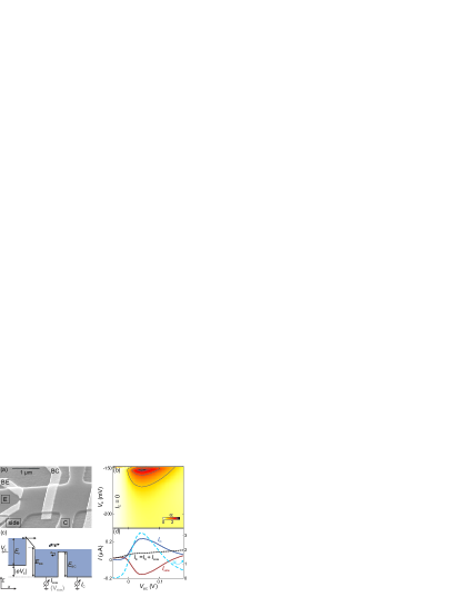
has been fabricated from a GaAs/AlGaAs heterostructure which contains a 2DES 90 nm below the surface. The sample consists of a hallbar with several ohmic contacts (not visible). Three terminals are used as emitter “E,” “side” contact, and collector C. Metallic gates (light gray) serve to define a broad collector barrier BC and an emitter QPC “BE” electrostatically. The use of a QPC as emitter is not crucial; very similar data have been taken with a broad emitter barrier instead. As sketched in Fig. 1(c), electrons are injected from the emitter E at potential into the region between BE and BC. By tuning BE near pinch-off, it is assured that the injected electrons have a kinetic energy close to ( is the Fermi energy). At first these hot electrons move ballistically towards BC. Eventually they scatter and excite additional electrons from the degenerate Fermi sea, thereby transferring part of their energy and momentum. Conduction-band holes in the Fermi sea are left behind [Fig. 1(c)]. The collector barrier separates excited electrons (which can pass the barrier) from the holes (which are reflected); the accumulation of holes causes a buildup of positive charge between BE and BC. The measured currents and are defined to be positive when electrons flow from the sample into the respective terminals, as would be expected in diffusive transport. Here, we tune our devices away from the diffusive-transport regime. In contrast to many previous publications Heiblum (1981); Brill and Heiblum (1994); Kaya et al. (1996) we reach a ballistic regime which is far from local thermal equilibrium.
The mobility and Fermi energy of the 2DES are (at ) and (carrier density ). In our case the elastic mean-free path m exceeds the dimensions of the nanostructure by far. Measurements shown here have been performed in a 3He cryostat at mK but comparable results have been obtained in a wide temperature range of K in similar samples.
To probe for amplification, we consider the transfer ratio with the current injected from E. As a typical example is plotted in Fig. 1(b) as a function of and . Amplification () is observed in a limited region which is framed by contour lines. We have already reached in a similar setup (here ). The actually measured currents and are shown in Fig. 1(d) for constant mV. For very negative , the collector barrier BC is closed, , and . As BC is opened, shows a broad maximum, exceeding . Hence, electrons are drawn in from the side contact (, ), making the device an electron jet pump. In the limit of a wide-open collector barrier (large ) the electron-hole selectivity is lost and the setup behaves similarly to a network of ohmic resistors.
Figure 2(a)
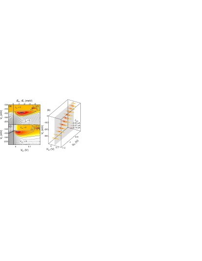
shows as a function of and [same raw data as Fig. 1(b)]. For BE is completely closed, hence, current flow is suppressed (). As is increased the emitter QPC opens and becomes nonzero. A dashed contour line encloses the region of . The three-dimensional (3D) representation in Fig. 2(b) displays a few contour lines at as a function of and for several emitter configurations . Clearly only occurs within a narrow tube in a region where the emitter QPC BE is almost pinched off.
The dependence of on the collector barrier height is also shown in Fig. 2(a) (top axis). can be determined from by measuring the reflection of Landau levels on the barrier in a magnetic field.Komiyama et al. (1989); Haug et al. (1988) In addition, the calibration point is known from linear-response transport measurements across the barrier as a function of . A simple one-dimensional (1D) model predicts maximal amplification at exactly since in this case excited electrons would pass BC whereas holes would be reflected. Strikingly, in Fig. 2(a) (which almost coincides with ) occurs at (). This is related to the 2D character of the charge carriers which allows an angle distribution of momenta within the 2DES. A charge carrier can only pass BC if its forward momentum component perpendicular to the barrier fulfills . Compared to the 1D case the barrier has therefore to be lower in 2D for a significant portion of the excited electrons to pass. is thus expected at ,angle_effect which is in agreement with experimental data (angle effect). In a previous publication, at was reported,Kaya and Eberl (2007) though this was obtained with a very different calibration procedure.
As an alternative to measuring in a three-terminal setup, Fig. 2(c) shows detected at the floating side contact. In the diffusive regime would be expected (since ). However, as in the current measurement, scattering of the injected electrons occurs and causes in a region roughly comparable to that of in Fig. 2(a). Since this is a two-terminal setup [see sketch in Fig. 1(c)], the continuity equation forces . Electrons cannot escape to the side contact and, hence, the angle effect as described above must be absent. Nevertheless the maximum of is still observed at . This can be explained by means of a positive charge that builds up between BE und BC in steady state (in a current measurement this charge is at least partly neutralized by ). The positive charge causes a decrease in the local chemical potential. Electrons trying to escape via BC thus see a larger effective barrier, and hence, the maximum effect is again found at (charge effect).charge_effect
In Fig. 2(b) a semi-transparent plane perpendicular to the cross section of Fig. 2(a) marks constant . A detailed measurement of within this plane is plotted in the inset of Fig. 3(a).
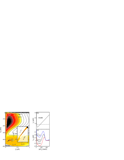
The main plot shows the same data as a function of and the overall current . We observe to the left of the dashed contour line. Figure 3(c) displays vertical cross sections of Fig. 3(a) which show the dependence of on the energy of the injected electrons for constant . The main behavior seen in Figs. 3(a) and 3(c) is closely related to the electron-electron scattering length . By numerical calculations based on the random-phase approximation, we have extended predictions for the linear-response regime Chaplik (1971); Giuliani and Quinn (1982) to the nonequilibrium case required for our experiments. The calculated is plotted in Fig. 3(b) for as a function of , the excess kinetic energy of the injected electrons. As expected, diverges for () and then rapidly decreases as is increased.Chaplik (1971); Giuliani and Quinn (1982) At higher , a minimum at is followed by a linear increase in which can be understood in terms of decreasing electron-electron interaction times.
This behavior can be mapped onto the measured energy dependence of [Fig. 3(c)] by taking into account the sample geometry [Fig. 1(a)]. The distance between BE and BC is nm [dashed line in Fig. 3(b)], about twice as long as the minimal calculated . In the extreme limits of or , we find and expect electrons to move ballistically and without electron-electron scattering within the sample. As the energy is increased starting from , decreases, and for , a positive charge builds up between BE and BC. It is neutralized by a growing negative component of [Fig. 3(c)]. Excited electrons always lose energy when scattering with the cold Fermi sea. Hence, scattering of an excited electron on the negative slope of [Fig. 3(b)] results in carriers with increased for subsequent scattering events. In contrast, scattering of electrons on the positive slope of often results in carriers with decreased . These carriers contribute heavily to a negative by multiple scattering events. The measured clearly is expected to extend to higher energies compared to the minimum of [Figs. 3(b) and 3(c)]. At larger energies the injected electrons tend to pass BC and scatter beyond the barrier. For only slightly larger than , some of the scattered electrons can travel back across BC and into the side contact, causing the local maximum of visible in Fig. 3(c). For even higher (mV, ) we find an extended regime with (). Here exceeds the sample dimensions by far so that electron-electron scattering happens far beyond BC, and all resulting charge carriers end up in the grounded collector contact C. This behavior () emphasizes the ballistic nature of the hot electrons in our experiments which goes beyond previously published results.Heiblum (1981); Brill and Heiblum (1994); Kaya et al. (1996)
Cross sections of Fig. 3(a) at constant excess kinetic energy allow us to discuss the dependence of on the total current and are displayed as line plots for mV in Fig. 4(a)
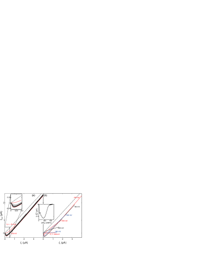
and for mV in Fig. 4(b). The dashed straight lines represent the expectation for ohmic behavior () with a slope determined by measuring the two-terminal resistances of the device in the linear-response regime. For and within the broad minimum of seen in Fig. 3(c) (mV), all curves coincide and are almost parallel to the ohmic line. This behavior is plausible for small enough when multiple scattering events and reflections, e. g. at BC, scramble the electrons. Under these conditions the initial momentum of the injected electrons becomes less important for the direction of current. However, in our case ohmic behavior is superimposed with a ballistic effect, a negative contribution to due to the separation of electrons and holes at BC.
As is increased from by adjusting , more and more electron-hole pairs are created and partly separated at BC. Only part of the positive charge of the holes can be neutralized from the side contact due to its finite resistance. The remaining positive charges lower the chemical potential of the Fermi sea between BE and BC (charge effect) so that less excited electrons escape via BC. The reflected electrons cause additional neutralization of holes. The neutralization rate therefore increases with increased , and the steady-state negative component of , reached when hole creation and neutralization rates balance, saturates for large . For higher energies and longer , deviations from this behavior occur as the injected electrons move forward ballistically [Fig. 4(b)].
The central inset in Fig. 4 displays as a function of the energy of the injected electrons. Similar to Fig. 3(c) it once again states the strong energy dependence of the amplification effect already discussed above. The local minima at meV and 72 meV are caused by emission of optical phonons. Sivan et al. (1989); Dzurak et al. (1992) They can also be seen in Fig. 3(c) and more distinct in Fig. 3(a) (two black arrows at and 72 meV).
Finally, it is important to differentiate the observed electronic Venturi effect from a thermoelectric effect caused by Joule heating. Such thermal effects are usually described within local equilibrium in the diffusive regime and mainly depend on the dissipated power. Figure 4 can be used to analyze as a function of power since is constant for each curve. The negative contribution to saturates as is increased, whereas in a thermoelectric effect it would be expected to grow further. The amplification ratios for thermally driven effects are also expected to be much smaller Brill and Heiblum (1994) compared to the we find, which again confirms the role of ballistic motion for the observed effects. In addition, the strong dependence of on the energy of the injected electrons [Fig. 3(a)], as well as the maximum occurring for [Fig. 2(a)], are in direct contradiction to an interpretation in terms of a thermoelectric effect.
As a result, we have built a prototype of an electron-avalanche amplifier. It is based on a jet pump explained by the electronic Venturi effect, namely, scattering of hot electrons with a degenerate Fermi liquid. Our systematic investigations go well beyond earlier publications and provide a comprehensive picture of the physics involved in the ballistic nonequilibrium regime. We present a consistent model based on electron-electron scattering and electron-hole neutralization which agrees qualitatively with our experimental results. Modifications in geometry and circuitry will result in improved electron jet pumps with potential applications, e. g., as a non-invasive charge detector. In such a device a single electron originating from a quantum dot would trigger a current pulse strong enough to be detected.
We thank J. P. Kotthaus, A. Govorov, L. Molenkamp, M. Heiblum, I. Kaya, and F. Marquardt for fruitful discussions. Financial support by the German Science Foundation via SFB 631, SFB 689, LU 819/4-1, and the German Israel program DIP, the German Excellence Initiative via the “Nanosystems Initiative Munich (NIM),” and LMUinnovativ (FuNS) is gratefully acknowledged.
References
- Govorov and Heremans (2004) A. O. Govorov and J. J. Heremans, Phys. Rev. Lett. 92, 026803 (2004).
- Bunsen (1869) R. Bunsen, Philos. Mag. 37, 1 (1869).
- Heiblum (1981) M. Heiblum, Solid-State Electron. 24, 343 (1981).
- Brill and Heiblum (1994) B. Brill and M. Heiblum, Phys. Rev. B 49, 14762 (1994).
- Kaya et al. (1996) I. I. Kaya et al., Semicond. Sci. Technol. 11, L135 (1996).
- (6) A. Palevski, C. P. Umbach, M. Heiblum, Appl. Phys. Lett. 55, 1421 (1989).
- Sivan et al. (1989) U. Sivan, M. Heiblum, and C. P. Umbach, Phys. Rev. Lett. 63, 992 (1989).
- Kaya and Eberl (2007) I. I. Kaya and K. Eberl, Phys. Rev. Lett. 98, 186801 (2007).
- Schinner et al. (2009) G. J. Schinner, H. P. Tranitz, W. Wegscheider, J. P. Kotthaus, S. Ludwig, Phys. Rev. Lett. 102, 186801 (2009).
- Dzurak et al. (1992) A. S. Dzurak, C. J. B. Ford, M. J. Kelly, M. Pepper, J. E. F. Frost, D. A. Ritchie, G. A. C. Jones, H. Ahmed, and D. G. Hasko, Phys. Rev. B 45, 6309 (1992).
- (11) H. Predel, H. Buhmann, L. W. Molenkamp, R. N. Gurzhi, A. N. Kalinenko, A. I. Kopeliovich, A. V. Yanovsky, Phys. Rev. B 62, 2057 (2000).
- Komiyama et al. (1989) S. Komiyama, H. Hirai, S. Sasa, and S. Hiyamizu, Phys. Rev. B 40, 12566 (1989).
- Haug et al. (1988) R. J. Haug, A. H. MacDonald, P. Streda, and K. von Klitzing, Phys. Rev. Lett. 61, 2797 (1988).
- (14) Simple estimations agree well with the observed magnitude of the angle effect.
- (15) In the regime where BE and BC are closed [top left corner of Fig. 2(c)], the side contact is electrically insulated. Here the potential is frozen at a constant value depending on the experimental history [in Fig. 2(c) we have performed vertical sweeps].
- Chaplik (1971) A. V. Chaplik, Zh. Eksp. Teor. Fiz. 60, 1845 (1971).
- Giuliani and Quinn (1982) G. F. Giuliani and J. J. Quinn, Phys. Rev. B 26, 4421 (1982).