Auger mediated quantum sticking of positrons to surfaces: Evidence for single step transition from a scattering state to a surface image potential bound state
Abstract
We present the observation of an efficient mechanism for positron sticking to surfaces termed here Auger mediated quantum sticking. In this process the energy associated with the positrons transition from an unbound scattering state to a bound image potential state is coupled to a valence electron which can then have sufficient energy to leave the surface. Compelling evidence for this mechanism is found in a narrow secondary electron peak observed at incident positron kinetic energies well below the electron work function.
pacs:
78.70.Bj, 71.60.+z, 68.47.De, 03.65.SqRecently positrons 1 have been shown to be very effective in probing surfaces and reduced dimensional systems such as nano-particles which possess high surface-to- volume ratios. If positrons become trapped in image potential surface states before annihilation, they can provide a means of selectively sampling the top most layer of a material or nanostructure due to the fact that such states typically extend about one atomic layer below the surface. Subsequent annihilation of surface trapped positrons with core or valence electrons results in signals (e.g. annihilation induced Auger electrons 2 or annihilation gamma rays 3 ) containing crucial information about the composition of the outermost regions of nano-materials.
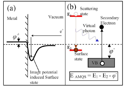
In this letter, we present experimental evidence for an efficient mechanism for depositing positrons directly into surface states through a single quantum step. In this process, the energy associated with the positron transition from an unbound scattering state to a bound surface state is coupled to a valence electron which may then have sufficient energy to leave the surface. Due to its similarity with the Auger transition in solids, this process has been termed as Auger mediated quantum sticking (AMQS). The quantum nature of the AMQS follows from the fact that the de Broglie wavelength of a eV positron (about Å) is an order of magnitude more than the width of the surface potential well (about 1 Å) 7 . Similar ideas have been suggested in theoretical models 4 ; 5 ; 6 , however no experimental evidence of this mechanism was available until now. The AMQS process schematized in Fig. 1 is related closely to the Auger de-excitation of atoms 8 or molecules 9 near surfaces, which has been studied for decades in various fields.
Here we provide direct experimental confirmation of the AMQS process through measurements of electron energy spectra resulting from very low energy positron bombardment ( eV). The strongest evidence for the AMQS is found in a narrow electron peak observed at incident positron kinetic energies well below the electron work function value. The present experiment also allowed us to determine the positron sticking probability as a function of incident particle energy and to obtain an independent measurement of the positron binding energy at the surface 10 . The fact that this new mechanism has an efficiency exceeding % at positron energies eV proves that it will be possible to use low energy positron beams to selectively probe the surfaces of fragile systems such as nano-particles and bio-materials and to obtain Auger signals which are completely free of secondary electron background.
The experiments were carried out using Time of Flight -Positron Annihilation induced Auger Electron Spectrometer (TOF-PAES) 11 which uses a magnetic bottle analyzer12 . Positrons from a Na-22 source are guided to the sample using an EB field. The emitted electrons are detected by a multi channel plate (MCP). The energy of the emitted electron was calculated from the electron time of flight (TOF) which was determined from the time difference between the electron and annihilation gamma ray detections (see Ref. 11 ). An Au sample (a % pure polycrystalline foil, mm thickness) was sputter cleaned every hours while a Cu(100) sample (a % pure single crystal mm diameter mm thickness) was sputter cleaned followed by annealing at oC every 12 hours. The incident beam profile at V sample bias was fitted with a Gaussian of eV FWHM and maximum at eV. % of the positrons have energy less than eV and this is referred to as the beam energy. The incident positron beam energy was increased by negatively biasing the sample.
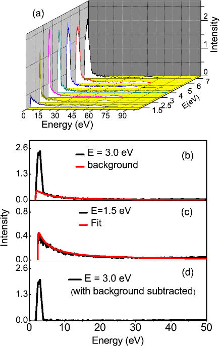
The primary evidence for the AMQS process in Cu is shown in Fig. 2(a), where the normalized energy spectrum taken at different positron beam energy (- eV) is plotted. In each spectrum the large peak at low energies ( eV) corresponds to electrons that are emitted as a result of positron impact at the sample surface. The much smaller peak at about eV is the PAES 2 .
AMQS can be distinguished from another process in which the final state of the incident positron is the bulk state. In the latter process, the maximum kinetic energy of the outgoing electron (as measured outside the sample surface) is given by
| (1) |
where is the incident positron energy (measured from the vacuum level) and = 4.65 (4.8) eV is the electron work function in Cu(Au) and = -0.02 (+0.9) eV is the positron work function [13-16]. Both work functions are measured from the vacuum level with positive sign below the vacuum level. The electrons can escape the sample if eV which implies that should be greater than . Hence, for incident positron kinetic energies of less than eV there should be no secondary electron emission according to this mechanism. In the case of AMQS, the positron excites an electron-hole pair while dropping to the surface state. The energy to dissipate is the initial positron kinetic energy plus the positron binding energy to the surface, thus we have
| (2) |
where is the surface binding energy of the positron measured from the vacuum level (with positive sign below the vacuum). Annihilation induced processes including Auger transitions and -ray emission can lead to the emission of electrons with energies as high as the Auger transition energy and keV respectively. However, such processes would lead to the formation of broad electron peaks. In our experiments, we found a narrow electron peak even when the incident kinetic energies of the positrons were less than eV. This can be explained from Eq. 2 by considering the process in which the electron excited from the Fermi sea escapes from the surface if the positron incident energy is greater than a certain threshold of about eV since is of the order of eV in most metals 15 .
Fig. 2(b) shows a typical electron spectrum of Cu. The large peak centered at eV corresponds to AMQS induced electrons. Fig. 2(c) shows the spectrum similar to Fig. 2(b) except the beam energy is below the threshold for electron emission, thus, one can notice the absence of the low energy (AMQS) peak: the quantum sticking is still taking place, but electron emission outside the sample is energetically prohibited. The same broad background between eV can be seen in both Figs 2(b) and 2(c). This feature is presumably the low energy electron tail associated with the PAES peak at eV. Fig. 2(d) shows the same spectrum of Fig. 2(b) but with the PAES background subtracted.
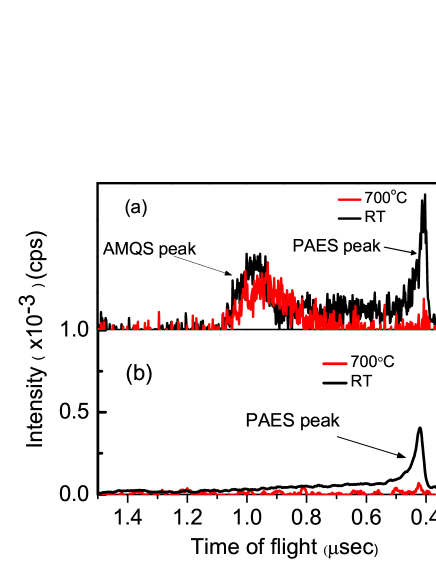
As a test to determine whether the low energy peak (AMQS peak) is due to a secondary effect of PAES or not, we have heated up the sample to oC and performed measurements with incident positron beam energy above (Fig. 3(a)) and below (Fig. 3(b)) the threshold given by Eq. 2 respectively. At oC, the positron trapped in the surface state is desorbed as positronium 15 . This prevents annihilation of the positron with core electrons and eliminates the PAES peak. Therefore, the presence of the AMQS peak at high temperature in Fig. 3(a) proves that this feature is not associated with the PAES process. Finally, the PAES peak always disappears at high temperature (as shown in Figs. 3(a) and 3(b)) while the AMQS peak disappears only when the beam energy is below threshold as given by Eq. 2.
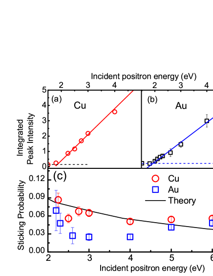
The AMQS peak integrated intensity with the background subtracted is plotted in Fig. 4 (a) and (b) as a function of the incident positron energy and it is used to estimate the surface state binding energy . Previous measurements of needed the monitoring of the fraction of incident positrons which forms positronium as a function of sample temperature 10 . Here, we fit the low energy part ( eV) of the AMQS peak integrated intensity with a linear function of the positron incident energy. The intercept of the straight line in conjunction with Eq. 2 is used to determine for Cu ( eV) and for Au (eV). This simple determination of agrees well with values reported in literature 16 .
The AMQS peak integrated intensity was also used to estimate the positron sticking probability . It has been assumed that the transition of the positron to the surface state is always associated to an electron-hole pair excitation. Hence, the sticking probability can be written as
| (3) |
where is the integrated intensity of the AMQS peak, is the number of incident positrons, is the escape probability for the excited electrons 18 and is that fraction of the excited electrons which have enough energy to escape by overcoming the workfunction . The ratio is therefore given by
| (4) |
where is the Fermi energy of the metal, , and is the density of states (DOS) 19 . The number of incident positrons was estimated using
| (5) |
where is the number of positrons trapped in the surface state, is the number of positrons that form positronium and is the number of positrons that are reflected from the surface. and are related by where is the fraction of incident positrons that form positronium (, determined as in Ref. 10 ), while where is the integrated intensity of PAES peak and is the probability that a positron trapped in the surface state will annihilate with a core electrons(%) 14 . Taking as the upper limit of 20 , the total number of incident positron can be written as
| (6) |
where is the fraction of Auger electrons for Cu (Au) that are transmitted to and detected by our analyzer. The sticking probability estimated in this way is plotted in Fig 4(c) and its trend agrees well with the calculations by Walker et al. 6 . This model predicts that will vanish as . However, this prediction cannot be resolved by the present experiment. Here we only focus on high positron surface sticking rates for non zero positron energies.
We have reported experiments that provide strong experimental evidence for a quantum sticking process in which an incident low energy positron makes a direct transitions from an unbound scattering state into an image potential surface state resulting in emission of a secondary electron. We have termed this process Auger mediated quantum sticking (AMQS) because the energy lost as the positron makes a transition to the bound state is given to an outgoing electron. Measurements of the incident beam energy at which the secondary peak first appears indicate a threshold almost eV lower than the value that would be expected if the positron were making a transition to a bulk state. These measurements were used to obtain the first estimates of the surface state binding energy at room temperature. The AMQS peak integrated intensity was used to estimate the sticking probability of positrons to surface and is found to be in qualitative agreement with the theory 6 . Our measurements provide the first experimental demonstration of the trapping of positrons into the surface state with high efficiencies (%) at incident positron energies below the threshold for collision induced secondary electron generation ( eV). We have used this effect to obtain the first Auger spectra that are completely free of background due to primary beam induced secondary electrons. These measurements also demonstrate the possibility of greatly reducing the beam induced surface damage associated with Auger analysis by using incident positron energies below the threshold of chemical bond breaking 21 . The strong signal associated with the AMQS process suggests that measurements of the AMQS intensity as a function of energy can provide an independent way of testing models for inelastic scattering and quantum sticking of light particles 22 ; 23 .
We acknowledge useful discussions with A.P. Mills Jr., P.M. Platzman and R.M. Nieminen. This work was supported in part by the NSF Grant No., Welch Foundation Grant No. Y- and the Ministry of Education and Science of the Russian Federation Grant No. and . B.B. was supported by Contract No. DE-FG02-07ER46352 from the Division of Materials Science and Engineering, Office of Science, U.S. Department of Energy and benefited from the allocation of computer time at the NERSC and the Northeastern University’s Advanced Scientific Computation Center.
References
- (1) S. Eijt et al., Nat. Mater. 5, 23 (2006).
- (2) A.H. Weiss et al., Phys. Rev. Lett. 61, 2245 (1988).
- (3) P. Asoka-Kumar et al., Phys. Rev. Lett. 77, 2097 (1996).
- (4) R. M. Nieminen in Positron beam and their applications edited by P. G. Coleman, World Scientific Singapore (2000).
- (5) M.J. Puska and R.M. Nieminen, Rev. Mod. Phys. 66, 841 (1994).
- (6) A. B. Walker et al., Phys. Rev. B 46, 1687 (1992).
- (7) A.P. Mills Jr, E.D. Shaw, M. Leventhal, P.M. Platzman, Phys. Rev. Lett. 66, 735 (1991).
- (8) H. D. Hagstrum, Phys. Rev. 96, 336 (1954).
- (9) B. Barbiellini and P.M. Platzman, New J. Phys. 8, 20 (2006).
- (10) A. P. Mills Jr, Solid State Comm. 31, 623 (1979); K. G. Lynn, Phys. Rev. Lett. 43, 391 (1979).
- (11) S. Xie, PhD Thesis, UT Arlington (2002).
- (12) P. Kruit and F. H. Read, J. Phys. E 16, 313 (1983).
- (13) A. P. Knights, P. G. Coleman, Surface Science 367, 238 (1996); M. Farjam and H. B. Shore, Phys. Rev. B 36, 5089 (1987).
- (14) N. Fazleev et al., Surface Science, 604, 32 (2010).
- (15) A. P. Mills Jr, proceedings LXXXIII International School of Physics Enrico Fermi, ed. by W. Brandt, A. Dupasquier, Academic Press, New York (1982).
- (16) M.J. Puska, R. M. Nieminen, Physica Scripta T4, 79 (1983).
- (17) The error bars are predominantly due to the uncertainty in the intercept as measured in figures 4(a) and (b).
- (18) is from Ref. 8 with and .
- (19) We have assumed a constant DOS near .
- (20) J. A. Baker, M. Touat and P.G. Coleman, J. Phys. C: Solid State Phys. 21, 4713 (1988).
- (21) A.H. Weiss et al., Rad. Phys. and Chem. 76 285 (2007); A. H. Weiss in the Proceedings of the International School of Physics Enrico Fermi, Physics of Many Positrons, IOP Press to be published.
- (22) K. W. Goodman and V. E. Henrich, Phys. Rev. B 49, 4827 (1994).
- (23) A. P. Mills Jr. and P.M. Platzman in New direction in antimatter chemistry and physics, edited by Clifford M. Surko and Franco A. Gianturco, Kluwer Academic Publishers (2001).