Bandstructure Effects in Ultra-Thin-Body DGFET: A Fullband Analysis
Abstract
1 Introduction
The interest in Ultra-Thin-Body (UTB) Double-Gate FET (DGFET) has grown in the recent past because of its superior properties compared to bulk MOSFET and is being considered as one of the future alternatives of present day bulk devices [1, 2]. Apart from superior gate control from both top and bottom, the intrinsic quantum confinement provided by its unique geometric structure affects the characteristics of UTB DGFET [3]. The different aspects of classical modeling of DGFETs have been discussed in [4, 5, 6]. There are a number of reports on the quantum mechanical effects on DGFET, both analytical as well as numerical [3, 7, 8, 9]. To solve numerically, one has to solve coupled Poisson-Schrodinger equations self-consistently [10]. This is done either by assuming some analytical relationship, or by taking full bandstructure into account. There has been considerable amount of work on calculation of bandstructure of materials [11, 12, 13, 14, 15, 16, 17] which can be plugged into the self-consistent Poisson-Schrodinger equation numerically [18].
DGFET has a unique property of volume inversion which improves the transport characteristics enormously [1], [3]. This can be explained with the help of quantum effects. Another important aspect is a substantial change in transport properties depending on the crystallographic orientation [19, 20, 21] which again can be analyzed from detailed bandstructure calculation. Also, the total number of intrinsic carriers reduces with the thinning of the channel material. This has an effect on the total gate capacitance of DGFET [22, 23, 24].
The aim of this paper is to focus on detailed analysis of some effects in UTB-DGFET which arise entirely because of bandstructure of the channel material and are not very apparent. Only Silicon has been considered as the thin channel material in this work, but this can be easily extended to other channel materials as well. The full-band structure calculation that has been used here is based on tight-binding method [14, 15, 16]. The calculated bandstructure has then been used to predict some intrinsic transport properties of thin film Si including band gap, density of states, intrinsic carrier concentration and effective mass. From this analysis, a number of features are explained which are unique to ultra-thin film semiconductors. Following this, Poisson-Schrodinger coupled equation is solved self-consistently taking care of the full bandstructure. With the help of this, volume inversion phenomenon has been critically analyzed with physical insights. This in turn throws some light on the spatial distribution of carriers inside the DGFET channel. Taking this into account, total channel capacitance and evolution of effective mass from source end to drain end along the channel have been analyzed.
The rest of the paper is organized as follows: Sec. 2 discusses on the details of tight-binding method of bandstructure calculation. The different intrinsic transport properties of ultra-thin film Silicon have been discussed in sec. 3. Poisson-Schrodinger coupled equation has been solved self-consistently and different related analyses have been performed in sec. 4. Finally the paper is concluded in sec. 5.
2 Bandstructure Calculation
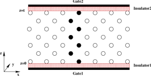
Tight-binding method of bandstructure calculation has been extensively studied by many researchers [11, 12, 13, 14, 15, 16, 17]. In this work, a 10-orbital tight-binding method [14, 15, 16] has been used to find bandstructure of the thin film Si, being used as channel material. Only the onsite energies and two-center overlap integrals of nearest neighbors have been taken into account. Spin orbit interaction has been neglected, and thus each point in the Brillouin zone is assumed to be degenerate with two spin states. Infinite crystal periodicity has been assumed along channel length and width directions and thus Bloch’s theorem is assumed to hold good in those directions. However, along the thickness of the channel, the crystal is truncated to a few monolayers, thus crystal periodicity can not be assumed in this direction. Suppose, the thickness contains atomic monolayers. Then, the truncated crystal can be formed by taking a basis of atoms along the thickness direction and spanning them over the whole 2-D space. Fig. 1 shows a monolayer thick channel with the basis atoms shown as black dots. The channel region can be formed by spanning the basis atoms along and . The tight-binding fitting parameters for Si, used in this work, have been taken from [15, 16]. An monolayers thick film will produce a tight-binding Hamiltonian [18]. To get rid of the huge number of surface states (whose energy eigen values often fall inside the semiconductor band gap) caused from dangling bonds, it has been assumed that the surfaces are completely passivated by Hydrogen. This has been achieved by artificially increasing the onsite energies of and orbitals of the surface atoms, as described in [17].
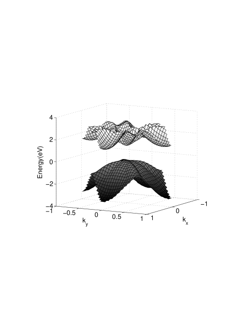
The assumption of this method is that the electronic wave function is strictly guided in the plane. Thus, the Brillouin zone will comprise of a -D space, as opposed to a -D one in bulk case. has been assumed to be zero throughout this paper. The whole -D Brillouin zone has been discretized using step size of for both and where is lattice constant (= for Si). In this paper, the film thickness has been referenced to the number of monolayers (AL) in the film. An AL thick Si film translates to a thickness of . Fig. 2 shows energy dispersion plot of a -monolayer thick (nm) film over the whole Brillouin zone. Only the top most valence subband and bottom most conduction subband have been included for clarity. Throughout this paper, the valleys occurring at point and at along direction are termed as valley and valley respectively.
3 Intrinsic Properties of Thin Film Si
In this section, the variations of different intrinsic electrical properties of thin film as a function of film thickness have been derived from the bandstructure calculation, described in the previous section.
3.1 Bandgap and Density of States
It has been well established in literature, by both theory and experiments, that in the nano-scale, bandgap of semiconductors is a function of size of the material. As size reduces, the bandgap of the material increases. Fig. 3 shows how the gap and gap of a Si film are changing as a function of the film thickness.
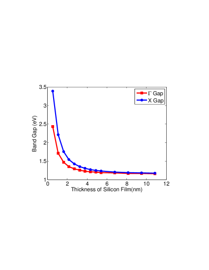
One should note that, for a sufficiently thin film, as opposed to the bulk case, the conduction band minimum occurs at direct point, and not in the direction. Thus the electrons will first populate the valley and hence, one can expect to see drastic change in transport properties for a thin film Si channel compared to bulk. As the film thickness increases, the energy difference between and valleys decreases, and electron will start populating both the valleys. Finally, at sufficiently large film thickness, at the bulk limit, valley is of less energy compared to valley, and thus, electrons will start populating only valley.
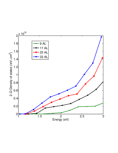
In Fig. 4, the -D density of states has been plotted as a function of electron energy in the conduction band, for different thickness values. In the calculation, the energy has been discretized in steps of eV. Just above the cut-off energy (conduction band minimum), only valley contributes. However, as energy increases, other regions of Brillouin zone also start contributing. As expected, density of states for thicker film is larger.
3.2 Intrinsic Carrier Concentration
As it has been discussed already that bandgap increases as the size goes from bulk to nano-scale, one expects lower intrinsic carrier concentration as the film thickness reduces. The per unit area intrinsic electron concentration at temperature is given by
| (1) |
where the first sum is over different subband indices of conduction band and the second sum is over all points in the first Brillouin zone. represents the energy eigenvalue at point of subband index. The Fermi-Dirac probability is given by
| (2) |
is the Boltzmann constant and is the chemical potential.
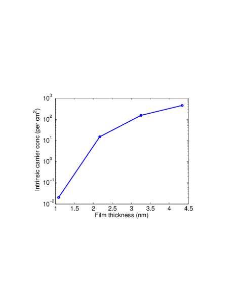
Fig. 5 shows that the intrinsic carrier concentration per unit area increases with film thickness. However, apart from the reduction in carrier concentration, another important observation is that the carriers have a distribution along the film thickness, which peaks at the center of the film. This is due to the spatial distribution of the wave function of the electronic states contributing to the carrier concentration. If the film of thickness has monolayers, then the film can be assumed to be discretized by points, at each of which, per unit volume carrier density is given by
| (3) |
where is the wave function of the electronic state at .
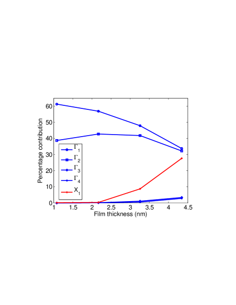
Fig. 6 plots the fractional contribution of different subbands to total electron concentration for a thin film of Si. and represent the subband of valley and subband of valley, respectively. It is clear that, for very small thickness, only and subbands contribute, but as thickness increases, other subbands also start contributing.
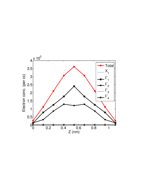
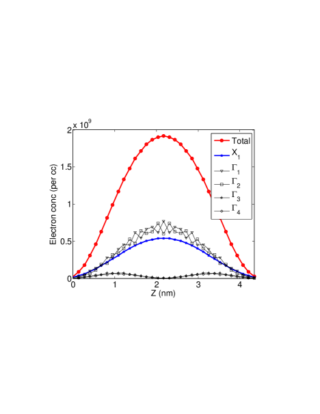
In Fig. 7 and 8, the spatial distribution of intrinsic carrier concentration, coming from different subbands, have been shown, for and monolayer thick Si film, respectively. Since for a monolayer thick film (nm), only and contribute, the spatial distribution of the total electron concentration is dictated by wavefunction distribution of only these two subands. The peak concentration comes at the middle of the film, and reduces as it approaches the surface. However, for a monolayer thick film (nm), subbands and bottom most subband contribute, and this in turn affects the total carrier distribution, as shown in Fig. 8.
3.3 Parabolic effective Mass and It’s Validity
A simple parabolic effective mass has been derived in this section at the minima of different subbands to show some interesting transport properties of thin film. Parabolic effective mass for the valley and subband is defined as
| (4) |
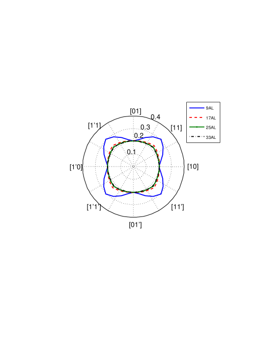
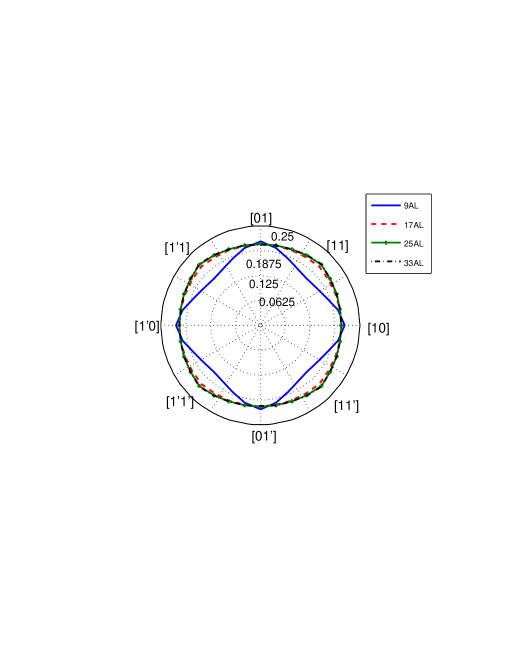
Fig. 9 and 10 show how parabolic effective mass (), normalized to electron rest mass (), calculated at the minima of two bottom most subbands and vary along different crystal direction, for four different film thicknesses. One should note that, in both cases, for monolayer thick film, effective mass is highly anisotropic. For , effective mass increases as one moves from direction to direction, whereas, it reduces for valley. However, for larger thickness, effective mass in both the valleys, becomes fairly isotropic.
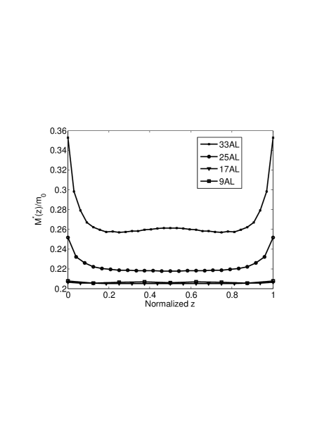
Since the effective masses vary with subbands, and electron concentration in different subbands has different spatial distributions, it is expected that effective mass should also have a spatial distribution. A ‘distributed effective mass’, say , a function of the depth along the thickness of the film, has been defined as:
| (5) |
where represents the fractional contribution of electron concentration at depth from subband of valley. This way of defining has the underlying assumption that all the electrons (more generally, an equal fraction of electrons from each subband of every valley) are moving along direction. Fig. 11 shows that for thinner films, is more or less uniform (which is because all the electrons are in and subbands possessing almost same effective mass), but as thickness increases, the effective mass at position closer to surface becomes larger than that of the central part of the film. Thus, for larger thickness, carriers closer to center of the film are expected to be more mobile than those which are closer to the surface. Note that, this effect is inherent to the intrinsic film, coming from spatial distribution of wave functions associated with different subbands. Another interesting observation is that, a monolayer thick film has (merginally) larger effective mass than a monolayer thick one at all . This is because of the fact that the valley has larger effective mass for monolayer thick film (Fig. 10).
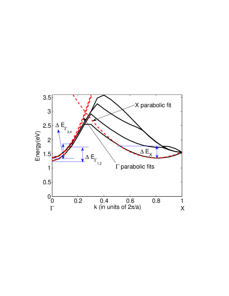
However, one should note that, parabolic effective mass approximation is valid only for electrons with smaller energy in the conduction band. The solid curves in Fig. 12 show the relationship along the direction for the four bottom most conduction subbands, calculated from tight-binding method, as described in sec. 2. The dotted curves show the fitted parabolic bands with same effective masses, as calculated from eqn. (4). represents the electronic energy range in the subband between which the parabolic tracks tight-binding fairly well. From Fig. 12, it is clearly visible that parabolic bands fail to track the actual bands for electron energies in excess of eV, referenced from corresponding band minimum, in all the cases. Nevertheless, the above simple analysis gives good qualitative insight about transport and mobility.
4 Self-consistent Solution of Poisson-Schrodinger Equation
To study the effect of gate voltage on this structure, a model device has been assumed consisting of a top gate and a bottom gate separated from the film by thin insulator layers, as shown in Fig. 1. The Si film is assumed to be undoped. Thus channel charge corresponds to only mobile charge. If is the potential at , then one can write the 1-D Poisson equation as [4, 10]
| (6) |
where is electronic charge, is permittivity of vacuum and is the relative permittivity of the channel material. The boundary conditions are derived from the fact that the normal component of the displacement vectors inside Si and insulators will be the same at and . Thus, at the boundaries, one can have
| (7) |
and
| (8) |
and are the relative permittivities of insulator1 and insulator2 respectively, and, and are corresponding thickness of the insulators. is the flatband voltage between the gate and channel. Eqn. (6) can be solved iteratively to find . To do this, first one assumes an initial potential profile , and then calculates bandstructure, which in turn provides the correction to . This is iterated until it converges. However, one should note that, in every iteration, one needs to calculate bandstructure. This is because the potential adds a dependent perturbation to the crystal potential, and thus both and are function of . This makes the problem computationally intensive.
To reduce computation, the following approximation has been made. Note that, the potential does not change drastically along (which is shown later), and thus, as far as change in bandstructure is concerned, it’s a fair assumption, that is constant (=) along . Suppose, is the original unperturbed tight-binding Hamiltonian, and are the unperturbed eigen values and eigen functions respectively. If one assumes that external potential only changes the on-site energies, and not overlap integrals, then the perturbation can be written as
| (9) |
where is diagonal unity matrix. Then,
| (10) |
which means that all the energy eigenvalues will be shifted by same energy (in other words, no relative change in energy eigenvalues), and the wave functions remain in the unperturbed state. Thus, it is sufficient to calculate the bandstructure only once, and the same and can be used through all the iterations. This reduces the total runtime by nearly same number of times as the number of iterations it takes to solve the Poisson equation (which varies roughly from to for different cases).
To validate the approximation, the amount of error being incurred in the worst case (maximum gate voltage where band bending is maximum) has been examined and the results are tabulated in Table 1, for both and monolayer thick films. The error here has been defined as where is the approximate value of parameter and is the exact value of the parameter.
| Thickness | ||||
|---|---|---|---|---|
| (AL) | Mean | SD | Mean | SD |
| 9 | -0.14 | 0.03 | 0.51 | 2.09 |
| 33 | 0.65 | 0.31 | 2.98 | 6.28 |
To simplify the analysis, in the following, the metals used as gate electrodes, have been assumed to have mid-gap work-function, and charge trapping inside insulators is taken to be zero. This essentially means that the flatband voltages and are taken to be zero. For simulation, it has been assumed that = = nm, = and = = .
4.1 Volume Inversion
Under the above mentioned assumption that bandstructure remains fairly the same under application of gate voltage, one can write the carrier density distribution as
| (11) |
where is the intrinsic carrier density at and is given by eqn. (3) and is the potential profile obtained by solving the eqn. (6). Fig. 13 and 14 show the distribution of carrier density over different subbands and the total density, for and atomic layer thick films respectively, when a V supply has been applied to both the gates. One should note the difference in shape of the carrier distribution as compared to intrinsic case. Also, the atomic layer thick film shows a higher peak carrier density compared to the atomic layer thick one, although the total integrated carrier concentration is larger for thicker film. This can be explained with ‘potential pinning’ effect, as discussed later. However, at any , the fractional contribution from a subband to the total carrier density remains the same at any applied gate voltage.
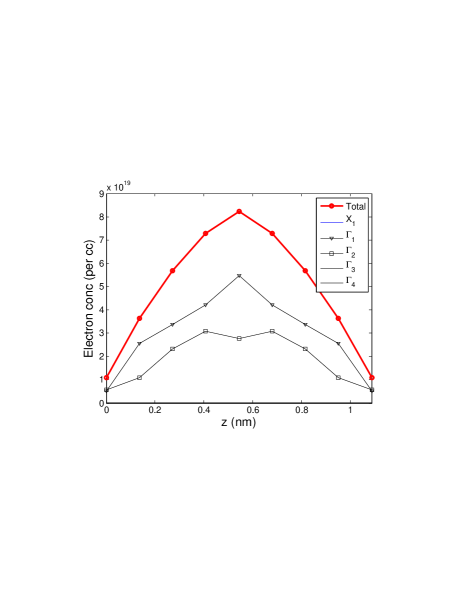
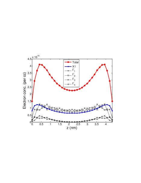
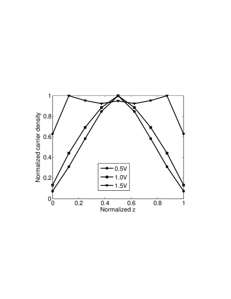
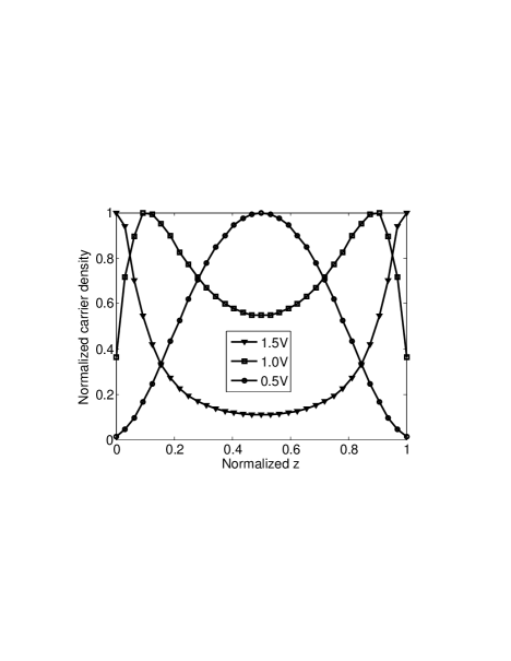
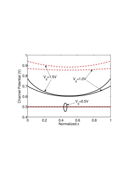
Fig. 15 and 16 show the normalized carrier distribution along the depth at different gate voltages, for and atomic layer thick films. The corresponding potential distribution plot is shown in Fig. 17. As gate voltage increases, the carriers of the ‘central-peaked’ channel start spreading toward the channel-insulator interface, and beyond a particular threshold gate voltage , the carrier distribution will start showing two ‘humps’ representing separation of peaks of carrier concentration inside channel. is defined by the condition
| (12) |
for a thinner film is expected to be larger than a thicker one. In other words, carriers try to stay closer to the center for thinner film. With increase in gate voltage, the shifting of carrier density peaks toward the gates can be thought of as a ‘carrier pulling effect’ of the gate voltage. The effect can be explained from the potential profile which is smaller at points closer to the center of the film. From eqn. (11), one notices that the overall carrier density profile arises from the individual contribution of the two terms and . peaks at the center of the film, and reduces toward the surface whereas follows the opposite trend. Thus, at sufficiently large voltage, it is possible that the peak of carrier density occurs at the surface, which is qualitatively same as the classical picture, where the exponential term dominates so much that the effect of ‘quantum mechanical’ distribution of intrinsic carrier density gets nullified.
As evident from Fig. 17, the potential profile for thinner films is more uniform, and actually ‘pinned’ at a higher value compared to the films of larger thickness leading to higher peak carrier concentration in thinner films as shown in Fig. 13 and 14.
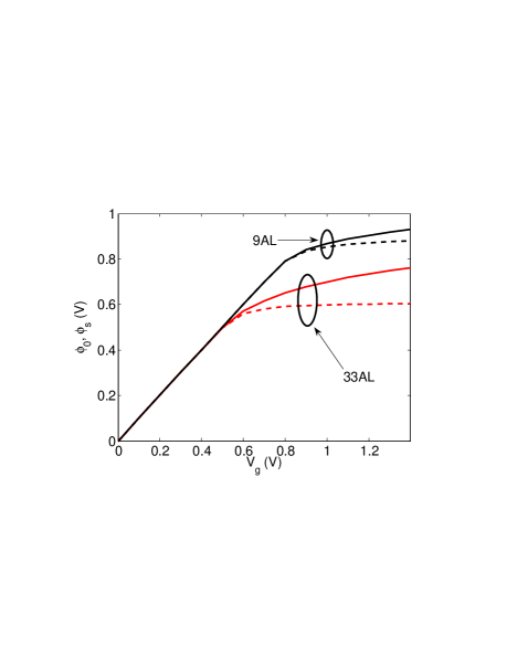
The above explanation becomes even more clarified from Fig. 18. Initially, for small gate voltage, both the surface potential and film center potential increase simultaneously at the same rate, and thus there will be only a single channel whose peak is at the center of the film. Beyond a certain gate voltage, and bifurcate, and saturates very quickly. However, keeps increasing, though at a much slower rate than earlier, causing higher carrier concentration at points closer to the surface, finally destroying the single peaked channel and creating two channels of ‘double hump’ shape. Note that, for atomic layer thick film, the ‘pinning’ voltages are higher than atomic layer film.
4.2 Channel Charge Distribution
The ‘carrier pulling effect’ explained in the previous section can have immense impact on the spatial distribution of total channel charge and hence device performance. Consider a DGFET where the source end is grounded and the drain is connected to which is same as applied gate voltage . At any point along the channel (with being taken as the source end), suppose the quasi-Fermi level is . can be assumed as independent of . Then, the Poisson equation in eqn. (6) gets modified as [6]
| (13) | |||||
where all references have been made from grounded source chemical potential. The carrier density should now be a function of as well, which in turn depends on the drain voltage. Deriving the exact drain current for a nano-MOSFET needs proper attention on transport model and the details will be communicated separately. However, to get a quantitative estimate, a long channel device (, ) with constant mobility has been assumed. The drain current and have been calculated using a similar procedure as in [6], by self-consistently solving eqn. (13) with drain current continuity equation. The extracted normalized carrier concentration is plotted over the whole channel region in Fig. 19 for different cases. At any , has been defined as
| (14) |
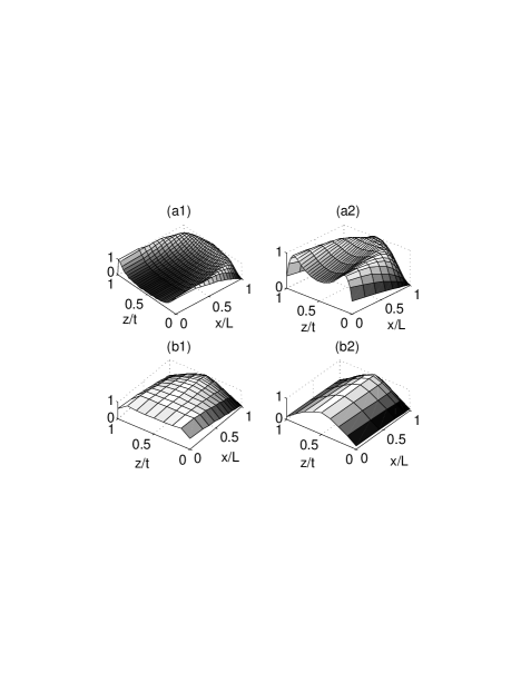
where represents the maximum value of over . The normalization is done in such a way which clearly shows the spatial shape of carrier distribution at different . It is observed that to the source end (), due to larger potential difference between gate and channel, there clearly exist two distinct carrier density peaks. However, as one moves toward the drain end, the potential difference between gate and channel reduces, and the two distinct peaks merge together producing a single center-peaked channel. Also, The magnitude of the total carrier concentration reduces toward the drain end. Putting in another way, near the source, carriers stay closer to the surface, and near the drain, carriers stay closer to the center of the channel. Thus, near the source, one expects more surface scattering and away from it, surface scattering is expected to reduce. Similar effects are true for gate leakage and gate capacitance, which can no longer be assumed to be uniform along the channel. It is evident from Fig. 19 that this effect is more pronounced in thicker channel devices, and at higher operating voltages. If the channel is thin enough, as is the case of (b2) in Fig. 19, it is possible to have a single peaked channel all over the device.
4.3 Evolution of Effective Mass Along DGFET Channel
In sec. 3, it has been discussed in detail how varies along the thickness for a thin film Si. Now, when one considers the channel of a DGFET, as has been discussed in the previous section, the potential difference between gate and channel changes from source end to drain end. Thus total number of carriers at different subbands also changes along the channel. Keeping this in mind, one can define an ‘average effective mass’,
| (15) |
which is basically harmonic average over the carriers along the thickness at a particular position along channel length. Physically, this indicates the ‘average’ effective mass of an electron located at distance from the source along the channel. Strictly speaking, eqn. (15) is valid only under the assumption that the vertical field is fairly constant and each electron suffers same scattering rate. Although this is not a very good approximation, but it gives an idea of how the channel charge distribution can affect spatial distribution of carrier effective mass.
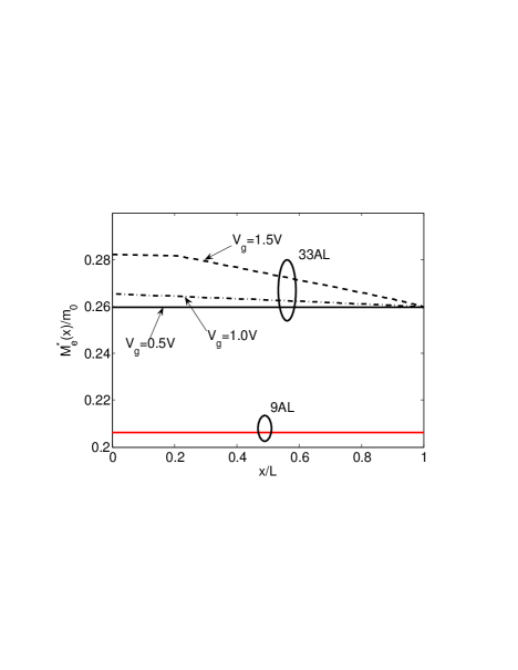
Fig. 20 shows for very small thickness channel (e.g. monolayer thick), hardly varies with as well as . However, for higher thickness, a gradual decrease in is observed from source end to drain end, and the effect is more prominent for higher gate voltages.
4.4 Channel Capacitance
Qualitatively, compared to classical analysis, the charge distribution in a quantum analysis, has two major differences: 1) The total charge in the channel reduces and 2) The charge distribution peak shifts from the surface toward the center of the film. The extent of the shift depends on the applied gate voltage. Both these effects cause a change in total gate capacitance [5]. The channel capacitance per unit volume at a depth can be defined as the rate of change of charge per unit volume with respect to the potential at that point. Mathematically,
| (16) |
where is given by
| (17) |
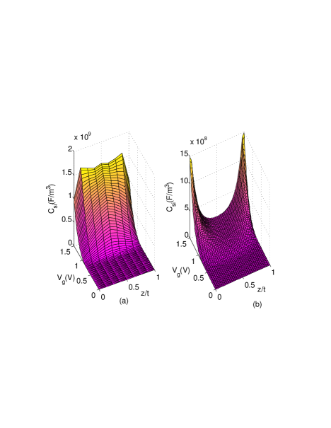
Fig. 21 shows the variations of channel capacitance with and . One should note that the position inside the film, where the coupling with gate is maximum, varies with gate voltage and as gate voltage increases, shifts toward the surface.
5 Conclusion
A detailed analysis of generic ultra-thin-body DGFET has been performed in this work. The channel material has been chosen to be Si, but the analysis and methodology can be readily extended to other promising channel materials as well. Ultra thin film of Si has been shown to have larger and direct band gap, as opposed to bulk. It has also been shown that the intrinsic carrier concentration is not only less compared to bulk, but also has a distribution over the channel thickness, peaking at the center. The contributions of different subbands from different valleys to both intrinsic carrier concentration as well as effective mass have been analyzed. The spatial distribution of distributed effective mass along thickness has been studied. It has also been shown that along direction, parabolic effective mass is fairly valid till an electronic energy of eV from the corresponding subband minima in all the relevant valleys. A detailed insightful analysis of volume inversion has been performed and using ‘carrier pulling effect’ of gate voltage, channel charge distribution in a DGFET has been predicted. The effects of channel charge distribution on effective mass and channel capacitance have been analyzed critically.
References
- [1] F. Balestra, “Double-gate silicon-on insulator transistor with volume inversion: a new device with greatly enhanced performance,” IEEE Elec. Dev. Lett., Vol. 8, No. 9, pp. 410, 1987.
- [2] J.G. Fossum et al., “Speed superiority of scaled double-gate CMOS,” IEEE Trans. on Electron Devices, Vol. 49, No. 5, pp. 808, 2002.
- [3] T. Ernst et al., “Ultimately thin Double-Gate SOI MOSFETs,” IEEE Trans. on Electron Devices, Vol. 50, No. 3, pp. 830, 2003.
- [4] Y. Taur, “An analytical solution to a Double-Gate MOSFET with undoped body,” IEEE Elec. Dev. Lett., Vol. 21, No. 5, pp. 245, 2000.
- [5] Y. Taur, “Analytic solutions of charge and capacitance in symmetric and asymmetric Double-Gate MOSFETs,” IEEE Trans. on Electron Devices, Vol. 48, No. 12, pp. 2861, 2001.
- [6] Y. Taur et al., “A continuous, analytic drain-current model for DG MOSFETs,” IEEE Elec. Dev. Lett., Vol. 25, No. 2, pp. 107, 2004.
- [7] T. Oussie, “Self-consistent quantum-mechanical calculations in ultrathin silicon-on-insulator structures,” J. Appl. Phys. 76 (1O), pp. 5989, 1994.
- [8] F. Gamiz et al., “Monte Carlo simulation of double-gate silicon-on-insulator inversion layers: The role of volume inversion,” J. Appl. Phys. 89 (1O), pp. 5478, 2001.
- [9] L. Ge et al., “Analytical modeling of quantization and volume inversion in thin Si-film DG MOSFETs,” IEEE Trans. on Electron Devices, Vol. 49, No. 2, pp. 287, 2002.
- [10] F. Stern, “Self-consistent results for n-type Si inversion layers,” Phys. Rev. B, Vol. 5, pp 4891, 1972.
- [11] J.C. Slater et al., “Simplified LCAO method for the periodic potential problem,” Phys. Rev., Vol. 94, pp. 1498, 1954.
- [12] D. J. Chadi et al., “Tight-binding calculations of the valence bands of diamond and zincblende crystals,” Phys. Stat. Sol. (b) 68, 405 (1975).
- [13] P. Vogl et al., “A semi-empirical tight-binding theory of the electronic structure of semiconductors,” J. Phys. Chem. Solids, Vol. 44, No. 5. pp. 365-378, 1983.
- [14] J.M. Jancu et al., “Empirical spds* tight-binding calculation for cubic semiconductors: General method and material parameters,” Phys. Rev. B, Vol. 57, pp 6493, 1998.
- [15] T.B. Boykin et al., “Diagonal parameter shifts due to nearest-neighbor displacements in empirical tight-binding theory,” Phys. Rev. B, Vol. 66, pp 125207, 2002.
- [16] T.B. Boykin et al., “Valence band effective-mass expressions in the empirical tight-binding model applied to a Si and Ge parametrization,” Phys. Rev. B, Vol. 69, pp. 115201, 2004.
- [17] S. Lee et al., “Boundary conditions for the electronic structure of finite-extent embedded semiconductor nanostructures,” Phys. Rev. B, Vol. 69, pp. 045316, 2004.
- [18] A. Rahman et al., “Novel channel materials for ballistic nanoscale MOSFETs - bandstructure effects,” IEDM Tech., pp. 601, 2005.
- [19] S. E. Laux, “Simulation study of Ge n-channel 7.5 nm DGFETs of arbitrary crystallographic alignment,” IEDM Tech., pp. 135, 2004.
- [20] A. Pethe et al., “Investigation of the performance limits of III-V double-gate n-MOSFETs,” IEDM Tech., pp. 605, 2005.
- [21] J. Steen et al., “Validity of the parabolic effective mass approximation in Silicon and germanium n-MOSFETs with different crystallographic orientations,” IEEE Trans. on Electron Devices, Vol. 54, No. 8, pp. 1843, 2007.
- [22] D. Vasileska et al., “Scaled silicon MOSFET’s: degradation of the total gate capacitance,” IEEE Trans. on Electron Devices, Vol. 44, No. 4, pp. 584, 1997.
- [23] L. Ge et al., “On the gate capacitance limits of nanoscale DG and FD SOI MOSFETS,” IEEE Trans. on Electron Devices, Vol. 53, No. 4, pp. 753, 2006.
- [24] O. Moldovan et al., “Explicit analytical charge and capacitance models of undoped double-gate MOSFETs,” IEEE Trans. on Electron Devices, Vol. 54, No. 7, pp. 1718, 2007.